KR20190108041A - 데시메이트된 위상 검출기 회로에 대한 시스템 및 방법 - Google Patents
데시메이트된 위상 검출기 회로에 대한 시스템 및 방법 Download PDFInfo
- Publication number
- KR20190108041A KR20190108041A KR1020190008825A KR20190008825A KR20190108041A KR 20190108041 A KR20190108041 A KR 20190108041A KR 1020190008825 A KR1020190008825 A KR 1020190008825A KR 20190008825 A KR20190008825 A KR 20190008825A KR 20190108041 A KR20190108041 A KR 20190108041A
- Authority
- KR
- South Korea
- Prior art keywords
- decimated
- signal
- counter
- output
- bbpd
- Prior art date
- Legal status (The legal status is an assumption and is not a legal conclusion. Google has not performed a legal analysis and makes no representation as to the accuracy of the status listed.)
- Granted
Links
- 238000000034 method Methods 0.000 title claims abstract description 26
- 238000005096 rolling process Methods 0.000 claims abstract description 154
- 230000001965 increasing effect Effects 0.000 claims description 14
- 230000009977 dual effect Effects 0.000 claims description 6
- 238000010586 diagram Methods 0.000 description 17
- 239000003990 capacitor Substances 0.000 description 4
- 238000004590 computer program Methods 0.000 description 3
- 230000001186 cumulative effect Effects 0.000 description 3
- 238000002513 implantation Methods 0.000 description 3
- 238000012986 modification Methods 0.000 description 3
- 230000004048 modification Effects 0.000 description 3
- 230000008859 change Effects 0.000 description 2
- 230000007423 decrease Effects 0.000 description 2
- 239000007943 implant Substances 0.000 description 2
- 238000002347 injection Methods 0.000 description 2
- 239000007924 injection Substances 0.000 description 2
- 238000004519 manufacturing process Methods 0.000 description 2
- 230000008569 process Effects 0.000 description 2
- 238000009825 accumulation Methods 0.000 description 1
- 238000004364 calculation method Methods 0.000 description 1
- 230000000295 complement effect Effects 0.000 description 1
- 238000007796 conventional method Methods 0.000 description 1
- 230000000694 effects Effects 0.000 description 1
- 238000005516 engineering process Methods 0.000 description 1
- 230000002708 enhancing effect Effects 0.000 description 1
- 230000006870 function Effects 0.000 description 1
- 230000014509 gene expression Effects 0.000 description 1
- 238000011084 recovery Methods 0.000 description 1
- 230000035945 sensitivity Effects 0.000 description 1
- 239000000758 substrate Substances 0.000 description 1
- 230000007704 transition Effects 0.000 description 1
Images





Classifications
-
- H—ELECTRICITY
- H03—ELECTRONIC CIRCUITRY
- H03L—AUTOMATIC CONTROL, STARTING, SYNCHRONISATION OR STABILISATION OF GENERATORS OF ELECTRONIC OSCILLATIONS OR PULSES
- H03L7/00—Automatic control of frequency or phase; Synchronisation
- H03L7/06—Automatic control of frequency or phase; Synchronisation using a reference signal applied to a frequency- or phase-locked loop
- H03L7/08—Details of the phase-locked loop
- H03L7/085—Details of the phase-locked loop concerning mainly the frequency- or phase-detection arrangement including the filtering or amplification of its output signal
- H03L7/091—Details of the phase-locked loop concerning mainly the frequency- or phase-detection arrangement including the filtering or amplification of its output signal the phase or frequency detector using a sampling device
-
- H—ELECTRICITY
- H02—GENERATION; CONVERSION OR DISTRIBUTION OF ELECTRIC POWER
- H02M—APPARATUS FOR CONVERSION BETWEEN AC AND AC, BETWEEN AC AND DC, OR BETWEEN DC AND DC, AND FOR USE WITH MAINS OR SIMILAR POWER SUPPLY SYSTEMS; CONVERSION OF DC OR AC INPUT POWER INTO SURGE OUTPUT POWER; CONTROL OR REGULATION THEREOF
- H02M3/00—Conversion of DC power input into DC power output
- H02M3/02—Conversion of DC power input into DC power output without intermediate conversion into AC
- H02M3/04—Conversion of DC power input into DC power output without intermediate conversion into AC by static converters
- H02M3/06—Conversion of DC power input into DC power output without intermediate conversion into AC by static converters using resistors or capacitors, e.g. potential divider
- H02M3/07—Conversion of DC power input into DC power output without intermediate conversion into AC by static converters using resistors or capacitors, e.g. potential divider using capacitors charged and discharged alternately by semiconductor devices with control electrode, e.g. charge pumps
-
- H—ELECTRICITY
- H03—ELECTRONIC CIRCUITRY
- H03K—PULSE TECHNIQUE
- H03K21/00—Details of pulse counters or frequency dividers
- H03K21/08—Output circuits
-
- H—ELECTRICITY
- H03—ELECTRONIC CIRCUITRY
- H03K—PULSE TECHNIQUE
- H03K21/00—Details of pulse counters or frequency dividers
- H03K21/16—Circuits for carrying over pulses between successive decades
-
- H—ELECTRICITY
- H03—ELECTRONIC CIRCUITRY
- H03K—PULSE TECHNIQUE
- H03K21/00—Details of pulse counters or frequency dividers
- H03K21/38—Starting, stopping or resetting the counter
-
- H—ELECTRICITY
- H03—ELECTRONIC CIRCUITRY
- H03L—AUTOMATIC CONTROL, STARTING, SYNCHRONISATION OR STABILISATION OF GENERATORS OF ELECTRONIC OSCILLATIONS OR PULSES
- H03L7/00—Automatic control of frequency or phase; Synchronisation
- H03L7/06—Automatic control of frequency or phase; Synchronisation using a reference signal applied to a frequency- or phase-locked loop
- H03L7/08—Details of the phase-locked loop
- H03L7/085—Details of the phase-locked loop concerning mainly the frequency- or phase-detection arrangement including the filtering or amplification of its output signal
-
- H—ELECTRICITY
- H03—ELECTRONIC CIRCUITRY
- H03L—AUTOMATIC CONTROL, STARTING, SYNCHRONISATION OR STABILISATION OF GENERATORS OF ELECTRONIC OSCILLATIONS OR PULSES
- H03L7/00—Automatic control of frequency or phase; Synchronisation
- H03L7/06—Automatic control of frequency or phase; Synchronisation using a reference signal applied to a frequency- or phase-locked loop
- H03L7/08—Details of the phase-locked loop
- H03L7/085—Details of the phase-locked loop concerning mainly the frequency- or phase-detection arrangement including the filtering or amplification of its output signal
- H03L7/089—Details of the phase-locked loop concerning mainly the frequency- or phase-detection arrangement including the filtering or amplification of its output signal the phase or frequency detector generating up-down pulses
- H03L7/0891—Details of the phase-locked loop concerning mainly the frequency- or phase-detection arrangement including the filtering or amplification of its output signal the phase or frequency detector generating up-down pulses the up-down pulses controlling source and sink current generators, e.g. a charge pump
Landscapes
- Engineering & Computer Science (AREA)
- Power Engineering (AREA)
- Stabilization Of Oscillater, Synchronisation, Frequency Synthesizers (AREA)
- Logic Circuits (AREA)
- Dram (AREA)
Abstract
Description
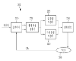
도 2a는 본 발명의 다양한 실시예에 따른 데시메이트된 BBPD 회로를 갖는 CDR을 도시한다.
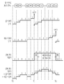
도 2b는 본 발명의 다양한 실시예에 따른 도 2a의 롤링 카운터의 동작의 타이밍 다이어그램을 도시한다.
도 2c는 본 발명의 다양한 실시예에 따른 데시메이트된 BBPD의 동작의 흐름도를 도시한다.
도 3은 본 발명의 다양한 실시예에 따른 타이밍 다이어그램을 도시한다.
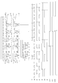
도 4는 여러가지 데시메이션(decimation) 기술을 사용하여 데시메이트되고 전하 펌프에 의해 적분된 BBPD의 업/다운 신호의 출력의 시뮬레이트된 도표(plot)를 도시한다.
도 5는 다양한 실시예에 따른 업 롤링 카운터 및 다운 롤링 카운터의 실시예를 도시한다.
도 6은 다양한 실시예에 따른 제1 롤링 카운터 스테이지(stage)에서의 이중 데이터 레이트(dual data rate, DDR) 인터페이스를 도시한다.
Claims (20)
- 뱅뱅 위상 검출기(BBPD);
상기 BBPD의 업(UP) 출력에 연결된 업 롤링 카운터;
상기 BBPD의 다운(DOWN) 출력에 연결된 다운 롤링 카운터; 및
상기 업 롤링 카운터 및 상기 다운 롤링 카운터에 연결되고, 상기 업 롤링 카운터로부터 데시메이트된(decimated) 업 신호를 수신하도록 구성되며, 상기 다운 롤링 카운터로부터 데시메이트된 다운 신호를 수신하도록 구성된 전하 펌프를 포함하고,
상기 전하 펌프는 상기 수신된 데시메이트된 업 신호 및 데시메이트된 다운 신호에 따라 제어 전압을 제공하도록 구성된, 데시메이트된 위상 검출기 회로. - 제1항에서,
상기 업 롤링 카운터는 상기 BBPD의 업 출력에 의해 업(UP)이 제공될 때마다 업 상태(UP state)를 증가시키도록 구성되고, 상기 다운 롤링 카운터는 상기 BBPD의 다운 출력에 의해 다운(DOWN)이 제공될 때마다 다운 상태(DOWN state)를 증가시키도록 구성된, 데시메이트된 위상 검출기 회로. - 제2항에서,
상기 업 롤링 카운터는 상기 업 롤링 카운터의 상기 업 상태가 0으로 롤 오버(roll over)될 때마다 상기 데시메이트된 업 신호를 출력하도록 구성되고,
상기 다운 롤링 카운터는 상기 다운 롤링 카운터의 상기 다운 상태가 0으로 롤 오버될 때마다 상기 데시메이트된 다운 신호를 출력하도록 구성된, 데시메이트된 위상 검출기 회로. - 제3항에서,
상기 업 롤링 카운터는
상기 BBPD의 상기 업 출력에 연결된 업 리플 카운터; 및
상기 업 리플 카운터의 출력에 연결된 업 폴링 에지 검출기를 포함하고, 상기 업 폴링 에지 검출기는 상기 업 리플 카운터가 롤 오버할 때 상기 데시메이트된 업 신호를 출력하도록 구성되며,
상기 다운 롤링 카운터는
상기 BBPD의 상기 다운 출력에 연결된 다운 리플 카운터; 및
상기 다운 리플 카운터의 출력에 연결된 다운 폴링 에지 검출기를 포함하고, 상기 다운 폴링 에지 검출기는 상기 다운 리플 카운터가 롤 오버할 때 상기 데시메이트된 다운 신호를 출력하도록 구성된, 데시메이트된 위상 검출기 회로. - 제4항에서,
상기 BBPD는 이중 데이터 레이트 BBPD를 포함하고,
상기 업 리플 카운터 및 다운 리플 카운터는 이중 데이터 레이트 인터페이스를 포함하는, 데시메이트된 위상 검출기 회로. - 제1항에서,
상기 전하 펌프는 전체 데시메이트된 업 신호에서 전체 데시메이트된 다운 신호를 뺀 값을 저장하도록 구성된 적분기를 포함하는, 데시메이트된 위상 검출기 회로. - 제1항에서,
상기 업 롤링 카운터는 상기 BBPD로부터 수신된 매 2N번째 업 신호 후에 상기 데시메이트된 업 신호를 출력하도록 구성된 업 N-비트 롤링 카운터를 포함하고,
상기 다운 롤링 카운터는 상기 BBPD로부터 수신된 매 2N번째 다운 신호 후에 상기 데시메이트된 다운 신호를 출력하도록 구성된 다운 N-비트 롤링 카운터를 포함하는, 데시메이트된 위상 검출기 회로. - 제7항에서,
상기 업 N-비트 롤링 카운터는 상기 BBPD로부터 수신된 매 네번째 업 신호 후에 상기 데시메이트된 업 신호를 출력하도록 구성된 업 2-비트 롤링 카운터를 포함하고,
상기 다운 N-비트 롤링 카운터는 상기 BBPD로부터 수신된 매 네번째 다운 신호 후에 상기 데시메이트된 다운 신호를 출력하도록 구성된 다운 2-비트 롤링 카운터를 포함하는, 데시메이트된 위상 검출기 회로. - 제1항에서,
상기 제어 전압에 따라 클럭을 생성하도록 구성된 전압 제어 발진기를 더 포함하는, 데시메이트된 위상 검출기 회로. - 업 롤링 카운터에서, 뱅뱅 위상 검출기(BBPD)로부터 업(UP) 신호를 수신하고, 수신된 각각의 업 신호에 대한 업 상태(UP state)를 증가시키는 단계;
다운 롤링 카운터에서, 상기 BBPD로부터 다운(DOWN) 신호를 수신하고, 수신된 각각의 다운 신호에 대한 다운 상태(DOWN state)를 증가시키는 단계;
상기 업 롤링 카운터에 의해, 상기 업 롤링 카운터의 상기 업 상태가 0으로 롤 오버(roll over)될 때마다 데시메이트된(decimated) 업 신호를 제공하는 단계; 및
상기 다운 롤링 카운터에 의해, 상기 다운 롤링 카운터의 상기 다운 상태가 0으로 롤 오버될 때마다 데시메이트된 다운 신호를 제공하는 단계를 포함하는, 뱅뱅 위상 검출기를 데시메이팅하는 방법. - 제10항에서,
전하 펌프에서, 전체 데시메이트된 다운 신호를 뺀 전체 데시메이트된 업 신호를 적분하는 단계를 더 포함하는, 뱅뱅 위상 검출기를 데시메이팅하는 방법. - 제11항에서,
상기 전하 펌프에 의해, 상기 전체 데시메이트된 다운 신호를 뺀 상기 전체 데시메이트된 업 신호에 따라 제어 전압을 제공하는 단계를 더 포함하는, 뱅뱅 위상 검출기를 데시메이팅하는 방법. - 제12항에서,
상기 제어 전압은 전압 제어 발진기에게 제공되는, 뱅뱅 위상 검출기를 데시메이팅하는 방법. - 제10항에서,
상기 업 롤링 카운터는
상기 BBPD의 업 출력에 연결된 업 리플 카운터; 및
상기 업 리플 카운터의 출력에 연결된 업 폴링 에지 검출기를 포함하고, 상기 업 폴링 에지 검출기는 상기 업 리플 카운터가 0으로 롤 오버할 때 상기 데시메이트된 업 신호를 출력하도록 구성되며,
상기 다운 롤링 카운터는
상기 BBPD의 다운 출력에 연결된 다운 리플 카운터; 및
상기 다운 리플 카운터의 출력에 연결된 다운 폴링 에지 검출기를 포함하고, 상기 다운 폴링 에지 검출기는 상기 다운 리플 카운터가 0으로 롤 오버할 때 상기 데시메이트된 다운 신호를 출력하도록 구성된, 뱅뱅 위상 검출기를 데시메이팅하는 방법. - 제10항에서,
상기 업 롤링 카운터는 상기 BBPD로부터 수신된 매 2N번째 업 신호 후에 상기 데시메이트된 업 신호를 출력하도록 구성된 업 N-비트 롤링 카운터를 포함하고,
상기 다운 롤링 카운터는 상기 BBPD로부터 수신된 매 2N번째 다운 신호 후에 상기 데시메이트된 다운 신호를 출력하도록 구성된 다운 N-비트 롤링 카운터를 포함하는, 뱅뱅 위상 검출기를 데시메이팅하는 방법. - 업 롤링 카운터에서, 뱅뱅 위상 검출기(BBPD)로부터 수신된 업(UP) 신호에 기반하여 업 상태(UP state)를 증가시키는 단계;
다운 롤링 카운터에서, 상기 BBPD로부터 수신된 다운(DOWN) 신호에 기반하여 다운 상태(DOWN state)를 증가시키는 단계;
상기 업 롤링 카운터에 의해, 상기 업 롤링 카운터의 상기 업 상태가 0으로 롤 오버(roll over)될 때마다, 데시메이트된(decimated) 업 신호를 전하 펌프에게 제공하는 단계;
상기 다운 롤링 카운터에 의해, 상기 다운 롤링 카운터의 상기 다운 상태가 0으로 롤 오버될 때마다, 데시메이트된 다운 신호를 상기 전하 펌프에게 제공하는 단계; 및
상기 전하 펌프에서, 전체 데시메이트된 다운 신호를 뺀 전체 데시메이트된 업 신호를 적분하는 단계를 포함하는, 뱅뱅 위상 검출기를 데시메이팅하는 방법. - 제16항에서,
상기 업 롤링 카운터는
상기 BBPD의 업 출력에 연결된 업 리플 카운터; 및
상기 업 리플 카운터의 출력에 연결된 업 폴링 에지 검출기를 포함하고, 상기 업 폴링 에지 검출기는 상기 업 리플 카운터의 상기 업 상태가 롤 오버될 때 상기 데시메이트된 업 신호를 출력하도록 구성된, 뱅뱅 위상 검출기를 데시메이팅하는 방법. - 제17항에서,
상기 다운 롤링 카운터는
상기 BBPD의 다운 출력에 연결된 다운 리플 카운터; 및
상기 다운 리플 카운터의 출력에 연결된 다운 폴링 에지 검출기를 포함하고, 상기 다운 폴링 에지 검출기는 상기 다운 리플 카운터의 다운 상태가 롤 오버될 때 상기 데시메이트된 다운 신호를 출력하도록 구성된, 뱅뱅 위상 검출기를 데시메이팅하는 방법. - 제16항에서,
상기 전하 펌프에 의해, 상기 전체 데시메이트된 다운 신호를 뺀 상기 전체 데시메이트된 업 신호에 따라 제어 전압을 제공하는 단계를 더 포함하는, 뱅뱅 위상 검출기를 데시메이팅하는 방법. - 제16항에서,
상기 업 롤링 카운터는 상기 BBPD로부터 수신된 매 2N번째 업 신호 후에 상기 데시메이트된 업 신호를 출력하도록 구성된 업 N-비트 롤링 카운터를 포함하고,
상기 다운 롤링 카운터는 상기 BBPD로부터 수신된 매 2N번째 다운 신호 후에 상기 데시메이트된 다운 신호를 출력하도록 구성된 다운 N-비트 롤링 카운터를 포함하는, 뱅뱅 위상 검출기를 데시메이팅하는 방법.
Applications Claiming Priority (4)
| Application Number | Priority Date | Filing Date | Title |
|---|---|---|---|
| US201862641911P | 2018-03-12 | 2018-03-12 | |
| US62/641,911 | 2018-03-12 | ||
| US16/109,645 | 2018-08-22 | ||
| US16/109,645 US10411593B1 (en) | 2018-03-12 | 2018-08-22 | Average and decimate operations for bang-bang phase detectors |
Publications (2)
| Publication Number | Publication Date |
|---|---|
| KR20190108041A true KR20190108041A (ko) | 2019-09-23 |
| KR102764004B1 KR102764004B1 (ko) | 2025-02-06 |
Family
ID=67843554
Family Applications (1)
| Application Number | Title | Priority Date | Filing Date |
|---|---|---|---|
| KR1020190008825A Active KR102764004B1 (ko) | 2018-03-12 | 2019-01-23 | 데시메이트된 위상 검출기 회로에 대한 시스템 및 방법 |
Country Status (3)
| Country | Link |
|---|---|
| US (1) | US10411593B1 (ko) |
| KR (1) | KR102764004B1 (ko) |
| CN (1) | CN110266307B (ko) |
Families Citing this family (4)
| Publication number | Priority date | Publication date | Assignee | Title |
|---|---|---|---|---|
| CN112187256B (zh) * | 2019-07-04 | 2023-08-25 | 智原微电子(苏州)有限公司 | 时钟数据恢复装置及其操作方法 |
| US11870880B2 (en) * | 2022-01-31 | 2024-01-09 | Samsung Display Co., Ltd. | Clock data recovery (CDR) with multiple proportional path controls |
| US11949423B2 (en) * | 2022-06-22 | 2024-04-02 | Faraday Technology Corp. | Clock and data recovery device with pulse filter and operation method thereof |
| CN116301196B (zh) * | 2023-03-22 | 2026-03-24 | 群联电子股份有限公司 | 时钟控制电路模块、存储器存储装置及时钟控制方法 |
Citations (2)
| Publication number | Priority date | Publication date | Assignee | Title |
|---|---|---|---|---|
| JPH11506884A (ja) * | 1995-06-07 | 1999-06-15 | アナログ・デバイセス・インコーポレーテッド | 位相ロック・ループのためのデジタル制御発振器 |
| US20100295586A1 (en) * | 2009-05-20 | 2010-11-25 | Xintronix Limited | Pll integral control |
Family Cites Families (10)
| Publication number | Priority date | Publication date | Assignee | Title |
|---|---|---|---|---|
| US4587496A (en) * | 1984-09-12 | 1986-05-06 | General Signal Corporation | Fast acquisition phase-lock loop |
| US6310521B1 (en) * | 1999-12-23 | 2001-10-30 | Cypress Semiconductor Corp. | Reference-free clock generation and data recovery PLL |
| US6630868B2 (en) | 2000-07-10 | 2003-10-07 | Silicon Laboratories, Inc. | Digitally-synthesized loop filter circuit particularly useful for a phase locked loop |
| US7916780B2 (en) | 2007-04-09 | 2011-03-29 | Synerchip Co. Ltd | Adaptive equalizer for use with clock and data recovery circuit of serial communication link |
| KR101199780B1 (ko) * | 2010-06-11 | 2012-11-12 | (주)에프씨아이 | 주파수 합성기의 주파수 보정 장치 및 그 방법 |
| US8798217B2 (en) | 2010-11-03 | 2014-08-05 | Qualcomm Incorporated | Method and digital circuit for recovering a clock and data from an input signal using a digital frequency detection |
| US9014322B2 (en) | 2012-05-23 | 2015-04-21 | Finisar Corporation | Low power and compact area digital integrator for a digital phase detector |
| US9716582B2 (en) | 2015-09-30 | 2017-07-25 | Rambus Inc. | Deserialized dual-loop clock radio and data recovery circuit |
| US9509319B1 (en) | 2016-04-26 | 2016-11-29 | Silab Tech Pvt. Ltd. | Clock and data recovery circuit |
| CN106972857B (zh) * | 2017-04-28 | 2023-03-21 | 深圳市国微电子有限公司 | 一种多环路自偏置锁相环电路及时钟产生器 |
-
2018
- 2018-08-22 US US16/109,645 patent/US10411593B1/en active Active
-
2019
- 2019-01-23 KR KR1020190008825A patent/KR102764004B1/ko active Active
- 2019-03-12 CN CN201910184088.XA patent/CN110266307B/zh active Active
Patent Citations (2)
| Publication number | Priority date | Publication date | Assignee | Title |
|---|---|---|---|---|
| JPH11506884A (ja) * | 1995-06-07 | 1999-06-15 | アナログ・デバイセス・インコーポレーテッド | 位相ロック・ループのためのデジタル制御発振器 |
| US20100295586A1 (en) * | 2009-05-20 | 2010-11-25 | Xintronix Limited | Pll integral control |
Also Published As
| Publication number | Publication date |
|---|---|
| US20190280591A1 (en) | 2019-09-12 |
| KR102764004B1 (ko) | 2025-02-06 |
| US10411593B1 (en) | 2019-09-10 |
| CN110266307A (zh) | 2019-09-20 |
| CN110266307B (zh) | 2022-05-06 |
Similar Documents
| Publication | Publication Date | Title |
|---|---|---|
| US8222936B2 (en) | Phase and frequency detector with output proportional to frequency difference | |
| KR20190108041A (ko) | 데시메이트된 위상 검출기 회로에 대한 시스템 및 방법 | |
| US9853634B2 (en) | Systems and methods of phase frequency detection with clock edge overriding reset, extending detection range, improvement of cycle slipping and/or other features | |
| US8284887B2 (en) | Clock data recovery circuit and multiplied-frequency clock generation circuit | |
| JP3299636B2 (ja) | ジッタが補償される低電力の位相ロック・ループとその方法 | |
| US8401140B2 (en) | Phase/frequency detector for a phase-locked loop that samples on both rising and falling edges of a reference signal | |
| US9632486B2 (en) | Masking circuit and time-to-digital converter comprising the same | |
| US6834093B1 (en) | Frequency comparator circuit | |
| US5818365A (en) | Serial to parallel conversion with phase locked loop | |
| US7459964B2 (en) | Switched capacitor filter and feedback system | |
| CN109478890B (zh) | 用于时钟相位生成的方法和装置 | |
| US8502581B1 (en) | Multi-phase digital phase-locked loop device for pixel clock reconstruction | |
| KR100728301B1 (ko) | 디지털로 제어 가능한 다중 위상 클럭 발생기 | |
| US6316982B1 (en) | Digital clock with controllable phase skew | |
| US6650146B2 (en) | Digital frequency comparator | |
| KR101000486B1 (ko) | 지연고정 루프 기반의 주파수 체배기 | |
| CN107579736B (zh) | 混合锁定检测器 | |
| CN114244350A (zh) | 加速充电帮浦及锁相回路以及其操作方法 | |
| US6707319B2 (en) | Frequency comparator with malfunction reduced and phase-locked state detecting circuit using the same | |
| US20040223574A1 (en) | Phase frequency detector used in digital PLL system | |
| KR20200109481A (ko) | 지연 없이 위상 주파수를 검출하는 장치 | |
| US11239849B2 (en) | Locked loop circuit and method with multi-phase synchronization | |
| CN113489488A (zh) | 锁相检测电路 | |
| CN111835344A (zh) | 锁相环电路及终端 | |
| JP2000278120A (ja) | ミスロック防止機能を有するdll回路 |
Legal Events
| Date | Code | Title | Description |
|---|---|---|---|
| PA0109 | Patent application |
Patent event code: PA01091R01D Comment text: Patent Application Patent event date: 20190123 |
|
| PG1501 | Laying open of application | ||
| A201 | Request for examination | ||
| PA0201 | Request for examination |
Patent event code: PA02012R01D Patent event date: 20211221 Comment text: Request for Examination of Application Patent event code: PA02011R01I Patent event date: 20190123 Comment text: Patent Application |
|
| E902 | Notification of reason for refusal | ||
| PE0902 | Notice of grounds for rejection |
Comment text: Notification of reason for refusal Patent event date: 20230824 Patent event code: PE09021S01D |
|
| E90F | Notification of reason for final refusal | ||
| PE0902 | Notice of grounds for rejection |
Comment text: Final Notice of Reason for Refusal Patent event date: 20240527 Patent event code: PE09021S02D |
|
| E701 | Decision to grant or registration of patent right | ||
| PE0701 | Decision of registration |
Patent event code: PE07011S01D Comment text: Decision to Grant Registration Patent event date: 20241226 |
|
| GRNT | Written decision to grant | ||
| PR0701 | Registration of establishment |
Comment text: Registration of Establishment Patent event date: 20250203 Patent event code: PR07011E01D |
|
| PR1002 | Payment of registration fee |
Payment date: 20250203 End annual number: 3 Start annual number: 1 |
|
| PG1601 | Publication of registration |