KR20190133461A - 센싱 회로 및 이를 포함하는 반도체 장치 - Google Patents
센싱 회로 및 이를 포함하는 반도체 장치 Download PDFInfo
- Publication number
- KR20190133461A KR20190133461A KR1020180058434A KR20180058434A KR20190133461A KR 20190133461 A KR20190133461 A KR 20190133461A KR 1020180058434 A KR1020180058434 A KR 1020180058434A KR 20180058434 A KR20180058434 A KR 20180058434A KR 20190133461 A KR20190133461 A KR 20190133461A
- Authority
- KR
- South Korea
- Prior art keywords
- line
- sensing
- signal
- sense amplifier
- bit line
- Prior art date
- Legal status (The legal status is an assumption and is not a legal conclusion. Google has not performed a legal analysis and makes no representation as to the accuracy of the status listed.)
- Granted
Links
Images



Classifications
-
- G—PHYSICS
- G11—INFORMATION STORAGE
- G11C—STATIC STORES
- G11C11/00—Digital stores characterised by the use of particular electric or magnetic storage elements; Storage elements therefor
- G11C11/21—Digital stores characterised by the use of particular electric or magnetic storage elements; Storage elements therefor using electric elements
- G11C11/34—Digital stores characterised by the use of particular electric or magnetic storage elements; Storage elements therefor using electric elements using semiconductor devices
- G11C11/40—Digital stores characterised by the use of particular electric or magnetic storage elements; Storage elements therefor using electric elements using semiconductor devices using transistors
- G11C11/401—Digital stores characterised by the use of particular electric or magnetic storage elements; Storage elements therefor using electric elements using semiconductor devices using transistors forming cells needing refreshing or charge regeneration, i.e. dynamic cells
- G11C11/4063—Auxiliary circuits, e.g. for addressing, decoding, driving, writing, sensing or timing
- G11C11/407—Auxiliary circuits, e.g. for addressing, decoding, driving, writing, sensing or timing for memory cells of the field-effect type
- G11C11/408—Address circuits
- G11C11/4085—Word line control circuits, e.g. word line drivers, - boosters, - pull-up, - pull-down, - precharge
-
- G—PHYSICS
- G11—INFORMATION STORAGE
- G11C—STATIC STORES
- G11C11/00—Digital stores characterised by the use of particular electric or magnetic storage elements; Storage elements therefor
- G11C11/21—Digital stores characterised by the use of particular electric or magnetic storage elements; Storage elements therefor using electric elements
- G11C11/34—Digital stores characterised by the use of particular electric or magnetic storage elements; Storage elements therefor using electric elements using semiconductor devices
- G11C11/40—Digital stores characterised by the use of particular electric or magnetic storage elements; Storage elements therefor using electric elements using semiconductor devices using transistors
- G11C11/401—Digital stores characterised by the use of particular electric or magnetic storage elements; Storage elements therefor using electric elements using semiconductor devices using transistors forming cells needing refreshing or charge regeneration, i.e. dynamic cells
- G11C11/4063—Auxiliary circuits, e.g. for addressing, decoding, driving, writing, sensing or timing
- G11C11/407—Auxiliary circuits, e.g. for addressing, decoding, driving, writing, sensing or timing for memory cells of the field-effect type
- G11C11/409—Read-write [R-W] circuits
- G11C11/4091—Sense or sense/refresh amplifiers, or associated sense circuitry, e.g. for coupled bit-line precharging, equalising or isolating
-
- G—PHYSICS
- G11—INFORMATION STORAGE
- G11C—STATIC STORES
- G11C11/00—Digital stores characterised by the use of particular electric or magnetic storage elements; Storage elements therefor
- G11C11/21—Digital stores characterised by the use of particular electric or magnetic storage elements; Storage elements therefor using electric elements
- G11C11/34—Digital stores characterised by the use of particular electric or magnetic storage elements; Storage elements therefor using electric elements using semiconductor devices
- G11C11/40—Digital stores characterised by the use of particular electric or magnetic storage elements; Storage elements therefor using electric elements using semiconductor devices using transistors
- G11C11/401—Digital stores characterised by the use of particular electric or magnetic storage elements; Storage elements therefor using electric elements using semiconductor devices using transistors forming cells needing refreshing or charge regeneration, i.e. dynamic cells
- G11C11/4063—Auxiliary circuits, e.g. for addressing, decoding, driving, writing, sensing or timing
- G11C11/407—Auxiliary circuits, e.g. for addressing, decoding, driving, writing, sensing or timing for memory cells of the field-effect type
- G11C11/409—Read-write [R-W] circuits
- G11C11/4094—Bit-line management or control circuits
-
- G—PHYSICS
- G11—INFORMATION STORAGE
- G11C—STATIC STORES
- G11C11/00—Digital stores characterised by the use of particular electric or magnetic storage elements; Storage elements therefor
- G11C11/21—Digital stores characterised by the use of particular electric or magnetic storage elements; Storage elements therefor using electric elements
- G11C11/34—Digital stores characterised by the use of particular electric or magnetic storage elements; Storage elements therefor using electric elements using semiconductor devices
- G11C11/40—Digital stores characterised by the use of particular electric or magnetic storage elements; Storage elements therefor using electric elements using semiconductor devices using transistors
- G11C11/401—Digital stores characterised by the use of particular electric or magnetic storage elements; Storage elements therefor using electric elements using semiconductor devices using transistors forming cells needing refreshing or charge regeneration, i.e. dynamic cells
- G11C11/4063—Auxiliary circuits, e.g. for addressing, decoding, driving, writing, sensing or timing
- G11C11/407—Auxiliary circuits, e.g. for addressing, decoding, driving, writing, sensing or timing for memory cells of the field-effect type
- G11C11/409—Read-write [R-W] circuits
- G11C11/4097—Bit-line organisation, e.g. bit-line layout, folded bit lines
-
- G—PHYSICS
- G11—INFORMATION STORAGE
- G11C—STATIC STORES
- G11C11/00—Digital stores characterised by the use of particular electric or magnetic storage elements; Storage elements therefor
- G11C11/21—Digital stores characterised by the use of particular electric or magnetic storage elements; Storage elements therefor using electric elements
- G11C11/34—Digital stores characterised by the use of particular electric or magnetic storage elements; Storage elements therefor using electric elements using semiconductor devices
- G11C11/40—Digital stores characterised by the use of particular electric or magnetic storage elements; Storage elements therefor using electric elements using semiconductor devices using transistors
- G11C11/401—Digital stores characterised by the use of particular electric or magnetic storage elements; Storage elements therefor using electric elements using semiconductor devices using transistors forming cells needing refreshing or charge regeneration, i.e. dynamic cells
- G11C11/4063—Auxiliary circuits, e.g. for addressing, decoding, driving, writing, sensing or timing
- G11C11/407—Auxiliary circuits, e.g. for addressing, decoding, driving, writing, sensing or timing for memory cells of the field-effect type
- G11C11/409—Read-write [R-W] circuits
- G11C11/4099—Dummy cell treatment; Reference voltage generators
-
- G—PHYSICS
- G11—INFORMATION STORAGE
- G11C—STATIC STORES
- G11C2207/00—Indexing scheme relating to arrangements for writing information into, or reading information out from, a digital store
- G11C2207/002—Isolation gates, i.e. gates coupling bit lines to the sense amplifier
-
- G—PHYSICS
- G11—INFORMATION STORAGE
- G11C—STATIC STORES
- G11C7/00—Arrangements for writing information into, or reading information out from, a digital store
- G11C7/06—Sense amplifiers; Associated circuits, e.g. timing or triggering circuits
- G11C7/065—Differential amplifiers of latching type
Landscapes
- Engineering & Computer Science (AREA)
- Microelectronics & Electronic Packaging (AREA)
- Computer Hardware Design (AREA)
- Dram (AREA)
- Static Random-Access Memory (AREA)
- Semiconductor Memories (AREA)
Abstract
Description
도 2는 본 발명의 실시예에 따른 반도체 장치의 구성도.
도 3은 도 2의 반도체 장치에 관한 상세 구성도.
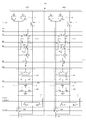
도 4는 도 3의 센싱회로에 관한 상세 회로도.
도 5는 도 3의 센싱회로에 관한 다른 실시예.
도 6은 도 3의 센싱회로에 관한 또 다른 실시예.
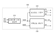
도 7은 도 3의 에지 구동부에 관한 상세 구성도.
도 8은 도 4의 에지 센싱 그룹에 관한 동작 타이밍도.
Claims (20)
- 센싱라인과 레퍼런스 라인에 인가된 데이터를 센싱 및 증폭하는 센스앰프;
분리신호에 대응하여 매칭라인과 상기 센싱라인 사이의 연결을 선택적으로 제어하는 제 1분리부;
상기 분리신호에 대응하여 상기 레퍼런스 라인과 비트라인 사이의 연결을 선택적으로 제어하는제 2분리부; 및
인에이블신호에 대응하여 상기 센싱라인의 데이터를 반전하여 상기 비트라인에 출력하는 반전부를 포함하는 센싱 회로. - 제 1항에 있어서, 상기 제 1분리부는
상기 센스앰프의 활성화 구간에서 상기 분리신호가 비활성화되어 상기 매칭라인과 상기 센싱라인 사이의 연결이 차단되는 센싱 회로. - 제 1항에 있어서, 상기 제 1분리부는
상기 매칭라인과 상기 센싱라인 사이에 연결되어 있으며, 게이트 단자를 통해 상기 분리신호가 인가되는 풀다운 구동소자를 포함하는 센싱 회로. - 제 1항에 있어서, 상기 제 2분리부는
상기 센스앰프의 활성화 구간에서 상기 분리신호가 비활성화되어 상기 레퍼런스 라인과 상기 비트라인 사이의 연결이 차단되는 센싱 회로. - 제 1항에 있어서, 상기 제 2분리부는
상기 레퍼런스 라인과 상기 비트라인 사이에 연결되어 있으며, 게이트 단자를 통해 상기 분리신호가 인가되는 풀다운 구동소자를 포함하는 센싱 회로. - 제 1항에 있어서, 상기 반전부는
상기 센싱라인의 출력에 대응하여 전원전압을 선택적으로 출력하는 제 1PMOS 트랜지스터;
상기 센싱라인의 출력에 대응하여 접지전압을 선택적으로 출력하는 제 1NMOS 트랜지스터:
상기 인에이블신호에 대응하여 상기 제 1NMOS 트랜지스터로부터 인가되는 전압을 상기 비트라인에 출력하는 제 2NMOS 트랜지스터; 및
상기 인에이블신호의 반전신호에 대응하여 상기 제 1PMOS 트랜지스터로부터 인가되는 전압을 상기 비트라인에 출력하는 제 2PMOS 트랜지스터를 포함하는 센싱 회로. - 제 1항에 있어서, 상기 반전부는
상기 센싱라인의 출력에 대응하여 상기 비트라인에 풀업 구동신호를 출력하는 제 3PMOS 트랜지스터; 및
상기 센싱라인의 출력에 대응하여 상기 비트라인에 풀다운 구동신호를 출력하는 제 3NMOS 트랜지스터를 포함하는 센싱 회로. - 제 1항에 있어서, 상기 반전부는
상기 센스앰프의 활성화 구간에서 상기 인에이블신호가 활성화되어 상기 센싱라인의 데이터를 반전하여 상기 비트라인에 재저장하는 센싱 회로. - 제 1항에 있어서,
상기 레퍼런스 라인의 로딩을 제어하는 로딩부를 더 포함하는 센싱 회로. - 제 9항에 있어서, 상기 로딩부는
드레인 단자와 소스 단자가 제 1전압의 인가단에 공통 연결되어 있으며 게이트 단자가 상기 레퍼런스 라인에 연결된 제 3PMOS 트랜지스터; 및
드레인 단자와 소스 단자가 상기 제 1전압의 인가단에 공통 연결되어 있으며 게이트 단자가 상기 레퍼런스 라인에 연결된 제 3NMOS 트랜지스터를 포함하는 센싱 회로. - 제 1항에 있어서,
상기 제 1전압은 전원전압(VDD)/2 레벨로 설정되는 센싱 회로. - 제 1항에 있어서,
상기 매칭라인은 전원전압(VDD)/2 레벨로 설정되는 센싱 회로. - 제 1항에 있어서,
리드 동작시 센스앰프에서 센싱된 전압을 입출력라인으로 전달하고, 라이트 동작시 상기 입출력라인으로부터 인가된 라이트 데이터를 상기 센스앰프에 전달하는 데이터 입출력부를 더 포함하는 센싱 회로. - 워드라인과 비트라인에 의해 선택된 데이터를 셀 어레이에 저장하는 매트; 및
복수의 센스앰프를 포함하여 센싱라인과 레퍼런스 라인에 인가된 데이터를 센싱 및 증폭하는 센싱회로를 포함하고,
상기 센싱회로는
상기 복수의 센스앰프의 센싱 동작시 분리신호에 대응하여 매칭라인과 상기 센싱라인 사이의 연결을 차단하고, 상기 레퍼런스 라인과 상기 비트라인 사이의 연결을 차단하는 반도체 장치. - 제 14항에 있어서,
상기 센싱회로는 최외곽 에지 영역에 배치되는 반도체 장치. - 제 14항에 있어서,
상기 센싱회로의 구동을 제어하기 위한 제어신호들을 생성하는 에지 구동부를 더 포함하는 반도체 장치. - 제 16항에 있어서, 상기 에지 구동부는
액티브신호와 프리차지신호에 대응하여 센스앰프 인에이블신호를 생성하는 인에이블신호 생성부;
상기 센스앰프 인에이블신호에 대응하여 센스앰프를 프리차지시키기 위한 이퀄라이징신호와, 상기 센스앰프를 구동하기 위한 구동신호를 생성하는 센스앰프 구동부; 및
상기 센스앰프 인에이블신호와 블록 어드레스에 대응하여 상기 분리신호와 인에이블신호를 생성하는 구동신호 생성부를 포함하는 반도체 장치. - 제 14항에 있어서, 상기 센싱 회로는
상기 센싱라인과 상기 레퍼런스 라인에 인가된 데이터를 센싱 및 증폭하는 상기 복수의 센스앰프;
상기 분리신호에 대응하여 상기 매칭라인과 상기 센싱라인 사이의 연결을 선택적으로 제어하는 제 1분리부;
상기 분리신호에 대응하여 상기 레퍼런스 라인과 상기 비트라인 사이의 연결을 선택적으로 제어하는 제 2분리부; 및
인에이블신호에 대응하여 상기 센싱라인의 데이터를 반전하여 상기 비트라인에 출력하는 반전부를 포함하는 반도체 장치. - 제 18항에 있어서,
상기 제 1분리부는 상기 센스앰프의 활성화 구간에서 상기 분리신호가 비활성화되어 상기 매칭라인과 상기 센싱라인 사이의 연결이 차단되고,
상기 제 2분리부는 상기 센스앰프의 활성화 구간에서 상기 분리신호가 비활성화되어 상기 레퍼런스 라인과 상기 비트라인 사이의 연결이 차단되는 반도체 장치. - 제 12항에 있어서,
상기 매칭라인은 전원전압(VDD)/2 레벨로 설정되는 반도체 장치.
Priority Applications (3)
| Application Number | Priority Date | Filing Date | Title |
|---|---|---|---|
| KR1020180058434A KR102471418B1 (ko) | 2018-05-23 | 2018-05-23 | 센싱 회로 및 이를 포함하는 반도체 장치 |
| US16/206,601 US10643687B2 (en) | 2018-05-23 | 2018-11-30 | Sensing circuit and semiconductor device including the same |
| CN201811495676.7A CN110534145B (zh) | 2018-05-23 | 2018-12-07 | 感测电路和包括其的半导体器件 |
Applications Claiming Priority (1)
| Application Number | Priority Date | Filing Date | Title |
|---|---|---|---|
| KR1020180058434A KR102471418B1 (ko) | 2018-05-23 | 2018-05-23 | 센싱 회로 및 이를 포함하는 반도체 장치 |
Publications (2)
| Publication Number | Publication Date |
|---|---|
| KR20190133461A true KR20190133461A (ko) | 2019-12-03 |
| KR102471418B1 KR102471418B1 (ko) | 2022-11-29 |
Family
ID=68613488
Family Applications (1)
| Application Number | Title | Priority Date | Filing Date |
|---|---|---|---|
| KR1020180058434A Active KR102471418B1 (ko) | 2018-05-23 | 2018-05-23 | 센싱 회로 및 이를 포함하는 반도체 장치 |
Country Status (3)
| Country | Link |
|---|---|
| US (1) | US10643687B2 (ko) |
| KR (1) | KR102471418B1 (ko) |
| CN (1) | CN110534145B (ko) |
Families Citing this family (3)
| Publication number | Priority date | Publication date | Assignee | Title |
|---|---|---|---|---|
| KR102730064B1 (ko) * | 2018-12-06 | 2024-11-15 | 에스케이하이닉스 주식회사 | 반도체 메모리 장치 및 그의 동작 방법 |
| KR102634614B1 (ko) * | 2019-07-12 | 2024-02-08 | 에스케이하이닉스 주식회사 | 수직형 메모리 장치 |
| US12014769B2 (en) | 2021-11-09 | 2024-06-18 | Samsung Electronics Co., Ltd. | Volatile memory device |
Citations (1)
| Publication number | Priority date | Publication date | Assignee | Title |
|---|---|---|---|---|
| US5608668A (en) * | 1995-12-22 | 1997-03-04 | Micron Technology, Inc. | Dram wtih open digit lines and array edge reference sensing |
Family Cites Families (9)
| Publication number | Priority date | Publication date | Assignee | Title |
|---|---|---|---|---|
| CA2217359C (en) * | 1997-09-30 | 2005-04-12 | Mosaid Technologies Incorporated | Method for multilevel dram sensing |
| KR100261217B1 (ko) * | 1997-11-21 | 2000-07-01 | 윤종용 | 반도체 메모리장치의 셀 어레이 제어장치 |
| US6301175B1 (en) * | 2000-07-26 | 2001-10-09 | Micron Technology, Inc. | Memory device with single-ended sensing and low voltage pre-charge |
| KR100393224B1 (ko) * | 2001-06-30 | 2003-07-31 | 삼성전자주식회사 | 비트라인 쌍들의 부하를 차단하는 회로를 구비하는 반도체메모리장치 |
| KR100410988B1 (ko) * | 2001-11-15 | 2003-12-18 | 삼성전자주식회사 | 반도체 메모리 장치 및 이 장치의 비트 라인 센싱 방법 |
| US6590819B1 (en) * | 2002-03-14 | 2003-07-08 | Micron Technology, Inc. | Digit line equilibration using time-multiplexed isolation |
| KR20100036596A (ko) | 2008-09-30 | 2010-04-08 | 삼성전자주식회사 | 에지 더미 셀들을 제거한 오픈 비트라인 구조의 반도체 메모리 장치 |
| KR102070977B1 (ko) | 2013-08-01 | 2020-01-29 | 삼성전자주식회사 | 감지 증폭기 및 그것을 포함하는 메모리 장치 |
| KR102562312B1 (ko) * | 2016-08-24 | 2023-08-01 | 삼성전자주식회사 | 비트라인 센스 앰프 |
-
2018
- 2018-05-23 KR KR1020180058434A patent/KR102471418B1/ko active Active
- 2018-11-30 US US16/206,601 patent/US10643687B2/en active Active
- 2018-12-07 CN CN201811495676.7A patent/CN110534145B/zh active Active
Patent Citations (1)
| Publication number | Priority date | Publication date | Assignee | Title |
|---|---|---|---|---|
| US5608668A (en) * | 1995-12-22 | 1997-03-04 | Micron Technology, Inc. | Dram wtih open digit lines and array edge reference sensing |
Also Published As
| Publication number | Publication date |
|---|---|
| KR102471418B1 (ko) | 2022-11-29 |
| US20190362767A1 (en) | 2019-11-28 |
| CN110534145B (zh) | 2023-06-30 |
| US10643687B2 (en) | 2020-05-05 |
| CN110534145A (zh) | 2019-12-03 |
Similar Documents
| Publication | Publication Date | Title |
|---|---|---|
| US10566036B2 (en) | Apparatuses and method for reducing sense amplifier leakage current during active power-down | |
| KR0177776B1 (ko) | 고집적 반도체 메모리 장치의 데이타 센싱회로 | |
| US6067256A (en) | Static semiconductor memory device operating at high speed under lower power supply voltage | |
| US7379378B2 (en) | Over driving control signal generator in semiconductor memory device | |
| US20190180812A1 (en) | Dynamic random access memory device | |
| US9627033B2 (en) | Sense amplifier and semiconductor device for securing operation margin of sense amplifier | |
| EP0278155B1 (en) | Dynamic random access memory | |
| CN110574109B (zh) | 感测放大器信号增强 | |
| KR100930384B1 (ko) | 입/출력라인 감지증폭기 및 이를 이용한 반도체 메모리장치 | |
| KR100295041B1 (ko) | 프리차지제어회로를구비하는반도체장치및프리차지방법 | |
| KR20220067206A (ko) | 반도체 메모리 장치의 센스 앰프 회로 | |
| JP5127435B2 (ja) | 半導体記憶装置 | |
| JP2729423B2 (ja) | 半導体記憶装置 | |
| US6320806B1 (en) | Input/output line precharge circuit and semiconductor memory device adopting the same | |
| CN100466099C (zh) | 包含能产生足够恒定延时信号的延时电路的半导体存储器 | |
| KR102471418B1 (ko) | 센싱 회로 및 이를 포함하는 반도체 장치 | |
| US7817491B2 (en) | Bank control device and semiconductor device including the same | |
| US6314045B1 (en) | Semiconductor memory device with a plurality of memory blocks | |
| JP2000182374A (ja) | ダイナミック型半導体メモリ | |
| KR100990140B1 (ko) | 반도체 메모리 소자 | |
| US6643201B2 (en) | Memory device having read charge control, write charge control and floating or precharge circuits | |
| US20250201299A1 (en) | Apparatuses and methods for conductive coupling of bit lines using bit line switches | |
| KR100203142B1 (ko) | 디램 | |
| JP2000348484A (ja) | 少なくとも一つのメモリーセルにカップリングされたシングルビットラインを有する強誘電体メモリ素子 | |
| KR100278924B1 (ko) | 센스 앰프 구동 바이어스 전위 프리차지 회로 |
Legal Events
| Date | Code | Title | Description |
|---|---|---|---|
| PA0109 | Patent application |
Patent event code: PA01091R01D Comment text: Patent Application Patent event date: 20180523 |
|
| PG1501 | Laying open of application | ||
| A201 | Request for examination | ||
| PA0201 | Request for examination |
Patent event code: PA02012R01D Patent event date: 20210421 Comment text: Request for Examination of Application Patent event code: PA02011R01I Patent event date: 20180523 Comment text: Patent Application |
|
| E902 | Notification of reason for refusal | ||
| PE0902 | Notice of grounds for rejection |
Comment text: Notification of reason for refusal Patent event date: 20220331 Patent event code: PE09021S01D |
|
| E701 | Decision to grant or registration of patent right | ||
| PE0701 | Decision of registration |
Patent event code: PE07011S01D Comment text: Decision to Grant Registration Patent event date: 20221012 |
|
| GRNT | Written decision to grant | ||
| PR0701 | Registration of establishment |
Comment text: Registration of Establishment Patent event date: 20221123 Patent event code: PR07011E01D |
|
| PR1002 | Payment of registration fee |
Payment date: 20221124 End annual number: 3 Start annual number: 1 |
|
| PG1601 | Publication of registration |