KR20200020260A - low resistance fingertip sensor and the method of making the same - Google Patents
low resistance fingertip sensor and the method of making the same Download PDFInfo
- Publication number
- KR20200020260A KR20200020260A KR1020180095732A KR20180095732A KR20200020260A KR 20200020260 A KR20200020260 A KR 20200020260A KR 1020180095732 A KR1020180095732 A KR 1020180095732A KR 20180095732 A KR20180095732 A KR 20180095732A KR 20200020260 A KR20200020260 A KR 20200020260A
- Authority
- KR
- South Korea
- Prior art keywords
- pattern
- parts
- connection
- electrodes
- portions
- Prior art date
- Legal status (The legal status is an assumption and is not a legal conclusion. Google has not performed a legal analysis and makes no representation as to the accuracy of the status listed.)
- Granted
Links
Images



Classifications
-
- G—PHYSICS
- G06—COMPUTING OR CALCULATING; COUNTING
- G06V—IMAGE OR VIDEO RECOGNITION OR UNDERSTANDING
- G06V40/00—Recognition of biometric, human-related or animal-related patterns in image or video data
- G06V40/10—Human or animal bodies, e.g. vehicle occupants or pedestrians; Body parts, e.g. hands
- G06V40/12—Fingerprints or palmprints
- G06V40/13—Sensors therefor
- G06V40/1306—Sensors therefor non-optical, e.g. ultrasonic or capacitive sensing
-
- H—ELECTRICITY
- H10—SEMICONDUCTOR DEVICES; ELECTRIC SOLID-STATE DEVICES NOT OTHERWISE PROVIDED FOR
- H10F—INORGANIC SEMICONDUCTOR DEVICES SENSITIVE TO INFRARED RADIATION, LIGHT, ELECTROMAGNETIC RADIATION OF SHORTER WAVELENGTH OR CORPUSCULAR RADIATION
- H10F39/00—Integrated devices, or assemblies of multiple devices, comprising at least one element covered by group H10F30/00, e.g. radiation detectors comprising photodiode arrays
- H10F39/10—Integrated devices
- H10F39/12—Image sensors
- H10F39/198—Contact-type image sensors [CIS]
-
- H01L27/14678—
-
- H01L24/03—
-
- H01L24/06—
-
- H—ELECTRICITY
- H10—SEMICONDUCTOR DEVICES; ELECTRIC SOLID-STATE DEVICES NOT OTHERWISE PROVIDED FOR
- H10W—GENERIC PACKAGES, INTERCONNECTIONS, CONNECTORS OR OTHER CONSTRUCTIONAL DETAILS OF DEVICES COVERED BY CLASS H10
- H10W72/00—Interconnections or connectors in packages
- H10W72/01—Manufacture or treatment
- H10W72/019—Manufacture or treatment of bond pads
-
- H—ELECTRICITY
- H10—SEMICONDUCTOR DEVICES; ELECTRIC SOLID-STATE DEVICES NOT OTHERWISE PROVIDED FOR
- H10W—GENERIC PACKAGES, INTERCONNECTIONS, CONNECTORS OR OTHER CONSTRUCTIONAL DETAILS OF DEVICES COVERED BY CLASS H10
- H10W72/00—Interconnections or connectors in packages
- H10W72/90—Bond pads, in general
Landscapes
- Engineering & Computer Science (AREA)
- Human Computer Interaction (AREA)
- Physics & Mathematics (AREA)
- General Physics & Mathematics (AREA)
- Multimedia (AREA)
- Theoretical Computer Science (AREA)
- Image Input (AREA)
- Measurement Of Length, Angles, Or The Like Using Electric Or Magnetic Means (AREA)
- Manufacturing & Machinery (AREA)
Abstract
Description
본 개시는 지문센서 및 그 제조 방법에 관한 것이다.The present disclosure relates to a fingerprint sensor and a method of manufacturing the same.
지문, 음성, 얼굴, 손 또는 홍채와 같은 개인의 고유한 특징을 이용한 개인 인증의 필요성은 점차 확대되고 있다. 개인 인증 기능은 금융 기기, 출입 통제기, 모바일 장치, 노트북 등에서 주로 사용되며, 최근 스마트 폰과 같은 모바일 장치가 널리 보급됨에 따라 스마트 폰 내에 저장된 많은 보안 정보를 보호하기 위해 개인 인증을 위한 지문 인식 장치가 채용되고 있다.The need for personal authentication using personal features such as fingerprint, voice, face, hand or iris is growing. The personal authentication function is mainly used in financial devices, access control devices, mobile devices, laptops, and the like. As mobile devices, such as smart phones, are widely used in recent years, fingerprint recognition devices for personal authentication are required to protect many security information stored in smart phones. It is adopted.
스마트 폰에는 터치 스크린 장치가 디스플레이 장치에 부착되어, 사용자에게 직관적인 입력 수단을 제공하고 있으며, 통상, 지문 인식 장치는 터치 스크린 장치와 별도로 마련되어 정해진 위치를 터치한 경우에만 지문 인식이 가능하다.In the smart phone, a touch screen device is attached to the display device to provide an intuitive input means to the user. In general, the fingerprint recognition device may be separately provided from the touch screen device, and fingerprint recognition may be performed only when a predetermined position is touched.
지문 인식 장치를 표시 패널 상에 구현하는 경우, 표시 패널의 영상이 잘 보이도록 투명 전극으로 지문 인식 장치의 전극을 구현할 수 있다. 하지만, 이와 같이 투명 전극 물질로 전극을 형성하는 경우 전극의 저항이 높아질 수 있다. 나아가, 표시 패널 영상의 해상도 및 지문 인식 장치의 감도를 높이기 위하여 전극의 크기를 작게 해야 하는 경우가 있는데, 이에 따라 투명 전극물질을 포함하는 전극의 저항은 더욱 높아질 수 있다.When the fingerprint recognition device is implemented on the display panel, the electrode of the fingerprint recognition device may be implemented as a transparent electrode so that an image of the display panel is easily seen. However, when the electrode is formed of the transparent electrode material as described above, the resistance of the electrode may be increased. Furthermore, in order to increase the resolution of the display panel image and the sensitivity of the fingerprint recognition device, it may be necessary to reduce the size of the electrode. Accordingly, the resistance of the electrode including the transparent electrode material may be further increased.
본 개시에 따른 다양한 실시예에 따라 사용자의 지문 패턴을 인식할 수 있는 금속 브릿지를 포함하는 지문 센서를 제공하고자 한다.According to various embodiments of the present disclosure, a fingerprint sensor including a metal bridge capable of recognizing a fingerprint pattern of a user is provided.
일 실시예에 따르면,According to one embodiment,
기판, 상기 기판 상에 마련되고, 복수 개의 제1 패턴부와 상기 복수 개의 제1 패턴부를 제1 방향을 따라 연결하는 복수 개의 제1 연결부를 포함하고 상기 제1 방향과 교차하는 방향인 제2 방향을 따라 반복적으로 배열되는 복수 개의 제1 전극, 상기 복수 개의 제1 전극 상에 마련되는 절연층 및 상기 절연층 상에 마련되고, 복수 개의 제2 패턴부와 상기 복수 개의 제2 패턴부를 상기 제2 방향을 따라 연결하는 복수 개의 제2 연결부를 포함하고 상기 제1 방향을 따라 반복적으로 배열되는 복수 개의 제2 전극을 포함하며 상기 제1 연결부 및 제2 연결부 중 적어도 어느 하나는 금속을 포함하는 지문 센서가 제공된다. A second direction provided on the substrate, the second direction including a plurality of first pattern parts and a plurality of first connection parts connecting the plurality of first pattern parts along a first direction and intersecting the first direction; A plurality of first electrodes repeatedly arranged along the plurality of layers; an insulating layer provided on the plurality of first electrodes; and a plurality of second pattern portions and the plurality of second pattern portions provided on the insulating layer. A fingerprint sensor including a plurality of second connectors connected along a direction, including a plurality of second electrodes repeatedly arranged along the first direction, and at least one of the first and second connectors includes a metal. Is provided.
상기 금속은 Pt, Ru, Au, Ag, Mo, Al, W, Pd, Mg, Ni, Nd, Ir, Cr, Ti, Mo 또는 Cu 등의 전도성 금속 또는 금속 합금 중 적어도 어느 하나를 포함할 수 있다.The metal may include at least one of a conductive metal or a metal alloy such as Pt, Ru, Au, Ag, Mo, Al, W, Pd, Mg, Ni, Nd, Ir, Cr, Ti, Mo, or Cu. .
상기 제1 연결부 및 제2 연결부 중 금속을 포함하지 않는 연결부는 상기 제1 패턴부 및 제2 패턴부가 포함하고 있는 물질과 동일한 물질을 포함할 수 있다.The connection part which does not contain a metal among the first connection part and the second connection part may include the same material as the material included in the first pattern part and the second pattern part.
상기 제1 연결부 및 제2 연결부는 모두 금속을 포함할 수 있다.Both the first connection part and the second connection part may include a metal.
상기 제1 패턴부 및 제2 패턴부는 투명 전도성 물질을 포함할 수 있다.The first pattern portion and the second pattern portion may include a transparent conductive material.
상기 투명 전도성 물질은 Oxide Metal Oxide(OMO)구조를 갖는 물질 및 ITO 중 적어도 어느 하나를 포함할 수 있다.The transparent conductive material may include at least one of a material having an oxide metal oxide (OMO) structure and ITO.
상기 제1 패턴부 및 제2 패턴부는 마름모 형상을 가질 수 있다.The first pattern portion and the second pattern portion may have a rhombus shape.
상기 제1 방향과 상기 제2 방향은 서로 수직일 수 있다.The first direction and the second direction may be perpendicular to each other.
다른 일 실시예에 따르면,According to another embodiment,
기판 상에, 복수 개의 제1 패턴부와 상기 복수 개의 제1 패턴부를 제1 방향을 따라 연결하는 복수 개의 제1 연결부를 포함하며 상기 제1 방향과 교차하는 방향인 제2 방향을 따라 반복적으로 배열되는 복수 개의 제1 전극을 형성하는 단계, 상기 복수 개의 제1 전극 상에 절연층을 형성하는 단계 및 상기 절연층 상에, 복수 개의 제2 패턴부와 상기 복수 개의 제2 패턴부를 제2 방향을 따라 연결하는 복수 개의 제2 연결부를 포함하며 상기 제1 방향을 따라 반복적으로 배열되는 복수 개의 제2 전극을 형성하는 단계를 포함하며, 상기 제1 연결부 및 제2 연결부 중 적어도 어느 하나는 금속을 포함하는 지문 센서 제조 방법이 제공된다.A plurality of first pattern portions and a plurality of first connection portions connecting the plurality of first pattern portions in a first direction on the substrate, and repeatedly arranged along a second direction which is a direction crossing the first direction. Forming a plurality of first electrodes, forming an insulating layer on the plurality of first electrodes, and forming a plurality of second pattern portions and the plurality of second pattern portions on the insulating layer in a second direction. And forming a plurality of second electrodes repeatedly arranged along the first direction, the second connecting parts including a plurality of second connecting parts connected to each other, and at least one of the first connecting parts and the second connecting parts includes a metal. A fingerprint sensor manufacturing method is provided.
상기 제1 전극층을 형성하는 단계는, 상기 기판 상에 복수 개의 상기 제1 패턴부를 먼저 형성한 후, 상기 제1 패턴부를 상기 제1 방향을 따라 연결하는 복수 개의 상기 제1 연결부를 상기 복수 개의 제1 패턴부들 사이에 형성할 수 있다.The forming of the first electrode layer may include forming a plurality of first pattern parts on the substrate first, and then connecting the first pattern parts along the first direction. It can be formed between one pattern portion.
상기 제1 전극층을 형성하는 단계는, 상기 기판 상에 복수 개의 상기 제1 연결부를 먼저 형성한 후, 상기 제1 패턴부들이 상기 제1 연결부들에 의해 상기 제1 방향을 따라 연결되도록 상기 복수 개의 제1 연결부들 사이에 상기 제1 패턴부들을 형성할 수 있다.The forming of the first electrode layer may include forming first plurality of first connection parts on the substrate, and then connecting the first pattern parts to be connected along the first direction by the first connection parts. The first pattern portions may be formed between the first connection portions.
상기 제2 전극층을 형성하는 단계는, 상기 기판 상에 복수 개의 상기 제2 패턴부를 먼저 형성한 후, 상기 제2 패턴부를 상기 제2 방향을 따라 연결하는 복수 개의 상기 제2 연결부를 상기 복수 개의 제2 패턴부들 사이에 형성할 수 있다.The forming of the second electrode layer may include forming a plurality of the second pattern parts on the substrate first, and then connecting the second pattern parts along the second direction. It can be formed between two pattern portions.
상기 제2 전극층을 형성하는 단계는, 상기 기판 상에 복수 개의 상기 제2 연결부를 먼저 형성한 후, 상기 제2 패턴부들이 상기 제2 연결부들에 의해 상기 제2 방향을 따라 연결되도록 상기 복수 개의 제2 연결부들 사이에 상기 제2 패턴부들을 형성할 수 있다.The forming of the second electrode layer may include forming the plurality of second connection parts on the substrate first, and then connecting the plurality of second pattern parts along the second direction by the second connection parts. The second pattern portions may be formed between the second connection portions.
상기 제1 연결부 및 제2 연결부 중 금속을 포함하지 않는 연결부는 상기 제1 패턴부 및 제2 패턴부가 포함하고 있는 물질과 동일한 물질을 포함할 수 있다.The connection part which does not contain a metal among the first connection part and the second connection part may include the same material as the material included in the first pattern part and the second pattern part.
상기 제1 연결부 및 제2 연결부는 모두 금속을 포함할 수 있다.Both the first connection part and the second connection part may include a metal.
본 개시에 따른 다양한 실시예는 금속 브릿지를 포함하여 전극의 저항값을 낮춘 지문센서를 제공할 수 있다.Various embodiments according to the present disclosure may provide a fingerprint sensor including a metal bridge to lower the resistance of an electrode.
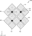
도 1은 일 실시예에 따른 지문 센서를 개략적으로 나타낸 평면도이다.
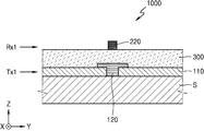
도 2는 도 1의 지문 센서의 A-A'부분을 개략적으로 나타낸 단면도이다.
도 3은 도 1의 지문 센서의 B-B'부분을 개략적으로 나타낸 단면도이다.
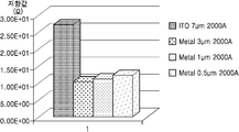
도 4는 도 1의 지문 센서가 포함하는 연결부의 종류 및 형상에 따른 지문 센서의 전극의 저항값을 비교한 그래프이다.
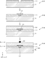
도 5는 일 실시예에 따른 지문 센서의 제조 방법을 단계적으로 도시한 것이다.
도 6은 다른 일 실시예에 따른 지문 센서의 제조 방법을 단계적으로 도시한 것이다.
도 7은 또 다른 일 실시예에 따른 지문 센서를 개략적으로 나타낸 평면도이다.
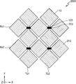
도 8은 또 다른 일 실시예에 따른 지문 센서를 개략적으로 나타낸 평면도이다. 1 is a plan view schematically illustrating a fingerprint sensor according to an exemplary embodiment.
FIG. 2 is a cross-sectional view schematically illustrating an AA ′ portion of the fingerprint sensor of FIG. 1.
3 is a cross-sectional view schematically illustrating a portion 'B-B' of the fingerprint sensor of FIG. 1.
4 is a graph comparing resistance values of electrodes of a fingerprint sensor according to the type and shape of a connection included in the fingerprint sensor of FIG. 1.
5 is a flowchart illustrating a method of manufacturing a fingerprint sensor according to an embodiment.
6 is a flowchart illustrating a method of manufacturing a fingerprint sensor according to another exemplary embodiment.
7 is a plan view schematically illustrating a fingerprint sensor according to another exemplary embodiment.
8 is a schematic plan view of a fingerprint sensor according to another exemplary embodiment.
아래에서는 첨부한 도면을 참조하여 다양한 실시예에 따른 저저항 지문센서 및 제조 방법에 대해 상세히 설명한다. 도면에서 동일한 참조부호는 동일한 구성요소를 지칭하며, 각 구성요소의 크기나 두께는 설명의 명료성을 위하여 과장되어 있을 수 있다.Hereinafter, a low resistance fingerprint sensor and a manufacturing method according to various embodiments will be described in detail with reference to the accompanying drawings. Like reference numerals in the drawings refer to like elements, and the size or thickness of each element may be exaggerated for clarity.
제 1, 제 2 등의 용어는 다양한 구성요소들을 설명하는데 사용될 수 있지만, 구성 요소들은 용어들에 의해 한정되어서는 안 된다. 용어들은 하나의 구성 요소를 다른 구성 요소로부터 구별하는 목적으로만 사용된다. 저저항 지문센서 및 제조 방법 는 여러 가지 상이한 형태로 구현될 수 있으며 여기에서 설명하는 실시예에 한정되지 않는다.Terms such as first and second may be used to describe various components, but the components should not be limited by the terms. The terms are used only to distinguish one component from another. The low resistance fingerprint sensor and the manufacturing method may be implemented in various different forms and are not limited to the embodiments described herein.
명세서 전체에서, 어떤 부분이 어떤 구성요소를 "포함"한다고 할 때, 이는 특별히 반대되는 기재가 없는 한 다른 구성요소를 제외하는 것이 아니라 다른 구성 요소를 더 포함할 수 있는 것을 의미한다.Throughout the specification, when a part is said to "include" a certain component, it means that it may further include other components, except to exclude other components unless specifically stated otherwise.
도 1은 일 실시예에 따른 지문 센서(1000)를 개략적으로 나타낸 평면도이다. 도 2는 도 1의 지문 센서의 A-A'부분을 개략적으로 나타낸 단면도이다. 도 3은 도 1의 지문 센서의 B-B'부분을 개략적으로 나타낸 단면도이다.1 is a plan view schematically illustrating a
도 1을 참조하면, 지문 센서(1000)는 제1 방향(Y축 방향)을 따라 나란하게 배치되어 있고, 제1 방향(Y축 방향)과 교차하는 방향인 제2 방향(X축 방향)을 따라 반복적으로 배열된 복수 개의 제1 전극(Tx1, Tx2) 및 제1 전극층(Tx1, Tx2) 상에 마련되고, 제2 방향(X축 방향)을 따라 나란하게 배치되어 있고, 제1 방향(Y축 방향)을 따라 반복적으로 배열된 복수 개의 제2 전극(Rx1, Rx2)을 포함할 수 있다.Referring to FIG. 1, the
제1 전극(Tx1, Tx2) 또는 제2 전극(Rx1, Rx2) 중에 어느 한 쪽에 외부로부터 전압이 인가될 수 있다. 제1 전극(Tx1, Tx2) 또는 제2 전극(Rx1, Rx2) 중에 어느 한쪽에 전압이 인가되면 제1 전극(Tx1, Tx2)과 제2 전극(Rx1, Rx2) 사이에 상호 전기용량(mutual capacitance)이 생성될 수 있다. 사용자가 제1 전극(Tx1, Tx2)과 제2 전극(Rx1, Rx2)중 어느 한쪽에 손가락을 이용하여 터치를 하게 되면 상기 터치된 전극의 터치 영역과 터치되지 않은 전극 사이에 생성되는 상호 전기용량의 변화가 발생할 수 있다. 상기 전기용량의 변화는 상기 사용자의 손가락의 표면의 지문이 나타내는 산(ridge)에 인접한 전극, 골(valley)에 인접한 전극에서 다르게 나타날 수 있다. 통상적으로 상기 손가락의 산, 골의 간격보다 전극 간의 간격을 더 좁게 함으로써 상기 손가락에 의한 상호 전기 용량의 변화를 위치별로 검출하여 지문 이미지를 연산할 수 있다. A voltage may be applied from the outside to either the first electrode Tx1 or Tx2 or the second electrode Rx1 or Rx2. When a voltage is applied to either one of the first electrodes Tx1 and Tx2 or the second electrodes Rx1 and Rx2, mutual capacitance is between the first electrodes Tx1 and Tx2 and the second electrodes Rx1 and Rx2. ) May be generated. When the user touches one of the first electrodes Tx1 and Tx2 and the second electrodes Rx1 and Rx2 by using a finger, the mutual capacitance generated between the touch area of the touched electrode and the non-touched electrode May change. The change in capacitance may appear differently at an electrode adjacent to a ridge and a valley near a valley indicated by a fingerprint on the surface of the user's finger. In general, a fingerprint image may be calculated by detecting a change in mutual capacitance caused by the fingers for each location by narrowing the distance between electrodes rather than the distance between the peaks and valleys of the finger.
복수 개의 제1 전극(Tx1, Tx2)은 외부로부터 전압을 인가받는 구동 전극일 수 있으며, 이 경우 제2 전극(Rx1, Rx2)은 전기 용량의 변화를 감지할 수 있는 측정부(미도시)가 연결되는 센싱 전극일 수 있다. 반대로, 제2 전극(Tx1, Tx2)이 외부로부터 전압을 인가받는 구동 전극일 수 있으며, 이 경우 제1 전극(Rx1, Rx2)은 전기 용량의 변화를 감지할 수 있는 측정부(미도시)가 연결되는 센싱 전극일 수 있다. 상기 센싱 전극이 상기 사용자의 손가락에 의해 터치되는 전극일 수 있다.The plurality of first electrodes Tx1 and Tx2 may be driving electrodes to which a voltage is applied from the outside. In this case, the second electrodes Rx1 and Rx2 may include a measuring unit (not shown) capable of detecting a change in capacitance. The sensing electrode may be connected. On the contrary, the second electrodes Tx1 and Tx2 may be driving electrodes to which a voltage is applied from the outside. In this case, the first electrodes Rx1 and Rx2 may include a measuring unit (not shown) capable of detecting a change in capacitance. The sensing electrode may be connected. The sensing electrode may be an electrode touched by a finger of the user.
도 2를 참조하면, 기판(S) 상에 복수 개의 제1 패턴부(110)가 서로 이격되도록 마련될 수 있다. 복수 개의 제1 패턴부(110) 사이에 형성된 복수 개의 공간에는 복수 개의 제1 연결부(120)가 마련될 수 있다. 이 경우, 복수 개의 제1 연결부(120)는 복수 개의 제1 패턴부(110)가 제1 방향(Y축 방향)을 따라 연결되도록 형성될 수 있다. 이와 같이, 복수 개의 제1 패턴부(110)가 복수 개의 제1 연결부(120)에 의해 상기 제1 방향(Y축 방향)을 따라 연결됨으로써 제1 전극(Tx1, Tx2)이 형성될 수 있다. 복수 개의 제1 전극(Tx1, Tx2)는 제2 방향(X축 방향)을 따라 반복적으로 배열될 수 있다. 제1 전극(Tx1) 상에는 절연층(300)이 형성될 수 있다. 절연층(300)상에는 제2 패턴부(210) 및 제2 연결부(220)를 포함하는 제2 전극(Rx1, Rx2)이 형성될 수 있다. 절연층(300)은 제1 패턴부(110) 및 제1 연결부(120)를 덮음으로써 제1 전극(Tx1, Tx2)과 제2 전극(Rx1, Rx2)을 서로 이격시킬 수 있다. 한편, A-A'단면을 통해서는 제2 전극(Rx1, Rx2) 중 제2 연결부(220)가 나타날 수 있다.Referring to FIG. 2, a plurality of
도 3을 참조하면, 절연층(300) 상에 복수 개의 제2 패턴부(210)가 서로 이격되도록 마련될 수 있다. 복수 개의 제2 패턴부(210) 사이에 형성된 복수 개의 공간에는 복수 개의 제2 연결부(220)가 마련될 수 있다. 이 경우, 복수 개의 제2 연결부(220)는 복수 개의 제2 패턴부(210)가 제2 방향(X축 방향)을 따라 연결되도록 형성될 수 있다. 이와 같이, 절연층(300) 상에는 복수 개의 제2 패턴부(210)가 복수 개의 제2 연결부(220)에 의해 제2 방향(X축 방향)을 따라 연결됨으로써 제2 전극(Rx1, Rx2)이 형성될 수 있다. 복수 개의 제2 전극(Rx1, Rx2)는 제1 방향(Y축 방향)을 따라 반복적으로 배열될 수 있다.Referring to FIG. 3, a plurality of
복수 개의 제1 전극(Tx1, Tx2)은 기판(S) 상에 마련되고, 복수 개의 제1 패턴부(110)와 복수 개의 제1 패턴부(110)를 상기 제1 방향(Y축 방향)을 따라 연결하는 복수 개의 제1 연결부(120)를 포함할 수 있다. 도 1에는 하나의 상기 제1 전극(Tx1, Tx2)이 세 개의 제1 패턴부(110)와 두 개의 제1 연결부(120)를 포함하고 있는 것이 도시되어 있으나, 제1 패턴부(110)와 제1 연결부(120)의 개수가 이에 한정되는 것은 아니며 도시된 것보다 더 많을 수 있다. 복수 개의 제1 전극(Tx1, Tx2)은 서로 평행하도록 제2 방향(X축 방향)을 따라 반복적으로 배열될 수 있다. 복수 개의 제1 전극(Tx1, Tx2) 상에는 절연층(300)이 마련될 수 있다.The plurality of first electrodes Tx1 and Tx2 are provided on the substrate S, and the plurality of
복수 개의 제2 전극(Rx1, Rx2)은 상기 절연층(300) 상에 마련되고, 복수 개의 제2 패턴부(210)와 복수 개의 제2 패턴부(210)를 상기 제1 방향(Y축 방향)과 교차하는 방향인 상기 제2 방향(X축 방향)을 따라 연결하는 복수 개의 제2 연결부(220)를 포함할 수 있다. 도 1에는 하나의 상기 제2 전극(Rx1, Rx2)이 세 개의 제2 패턴부(210)와 두 개의 제2 연결부(220)를 포함하고 있는 것이 도시되어 있으나, 제2 패턴부(210)와 제2 연결부(220)의 개수가 이에 한정되는 것은 아니며 도시된 것보다 더 많을 수 있다. 복수 개의 제2 전극(Rx1, Rx2)은 서로 평행하도록 제2 방향(Y축 방향)을 따라 반복적으로 배열될 수 있다.A plurality of second electrodes Rx1 and Rx2 are provided on the insulating
복수 개의 제1 패턴부(110) 및 복수 개의 제2 패턴부(210)는 투명 전도성 물질을 포함할 수 있다. 상기 투명 전도성 물질은 Oxide Metal Oxide (OMO)구조를 갖는 물질 및 ITO 중 적어도 어느 하나를 포함할 수 있다. 상기 투명 전도성 물질의 면저항은 1Ω 내지 20Ω일 수 있다. 또한 상기 투명 전도성 물질의 광 투과도는 70~95%일 수 있다.The plurality of
복수 개의 제1 패턴부(110) 및 복수 개의 제2 패턴부(210)는 마름모 형상을 포함할 수 있다. 그러나, 제1 패턴부(110) 및 제2 패턴부(210)의 패턴 형상은 마름모에 한정되는 것은 아니며 다른 여러 가지 다각형, 원형 등의 형상을 포함할 수 있다.The plurality of
도 1의 지문 센서(1000)는 각각 두 개의 제1 전극(Tx1, Tx2) 및 제2 전극(Rx1, Rx2)을 포함하고 있으나, 이에 한정되는 것은 아니며 두 개 이상의 제1 전극및 제2 전극(Rx1, Rx2)을 더 포함할 수 있다. The
제1 연결부(120) 및 제2 연결부(220) 둘 중 적어도 어느 하나는 금속을 포함할 수 있다. 상기 금속은 Pt, Ru, Au, Ag, Mo, Al, W, Pd, Mg, Ni, Nd, Ir, Cr, Ti, Mo 또는 Cu 등의 전도성 금속 또는 금속 합금을 포함할 수 있다. 제1 연결부(120) 및 제2 연결부(220)는 면저항 값이 0.01Ω 내지 1Ω이 되도록 두께 및 길이가 적절히 설정될 수 있다.At least one of the
복수 개의 제1 패턴부(110) 및 제2 패턴부(210)가 각각 금속을 포함하는 제1 연결부(120) 및 제2 연결부(220)로 연결되어 제1 전극(Tx1, Tx2) 및 제2 전극(Rx1, Rx2)의 면저항은, 제1 연결부(120) 및 제2 연결부(220)가 금속을 포함하지 않은 경우에 비해 낮아질 수 있다.The plurality of
도 4는 도 1의 지문 센서(1000)가 포함하는 연결부의 종류 및 형상에 따른 지문 센서의 전극의 저항값을 비교한 그래프이다.4 is a graph comparing resistance values of electrodes of a fingerprint sensor according to the type and shape of a connection part included in the
도 4를 참조하면, 제1 연결부(120) 또는 제2 연결부(220)가 투명 전도성 물질, 예를 들어 ITO를 포함한 경우와 금속을 포함하는 경우의 지문 센서의 전극의 저항값에 차이가 나타날 수 있다.Referring to FIG. 4, when the
우선, 제1 연결부(120) 또는 제2 연결부(220)가 투명 전도성 물질인 ITO를 포함하고 선 폭이 7㎛이고 도 1 내지 도 3의 Z축 방향 두께가 0.2㎛인 경우 전극의 저항값은 약 27Ω일 수 있다. First, when the
제1 연결부(120) 또는 제2 연결부(220)가 금속을 포함하는 경우에는 다음과 같이 세 가지 경우의 지문 센서의 전극의 저항값이 도시되어 있다. 우선, 제1 연결부(120) 또는 제2 연결부(220)의 선 폭이 3㎛이고 상기 Z축 방향 두께가 0.2㎛인 경우 단위 전극의 저항값은 약 10.4Ω일 수 있다. 또한, 제1 연결부(120) 또는 제2 연결부(220)의 선 폭이 1㎛이고 상기 Z축 방향 두께가 0.2㎛인 경우 전극의 저항값은 약 11.2Ω일 수 있다. 마지막으로, 제1 연결부(120) 또는 제2 연결부(220)의 선 폭이 3㎛이고 상기 Z축 방향 두께가 0.2㎛인 경우 전극의 저항값은 약 12.4Ω일 수 있다.When the
이와 같이, 제1 연결부(120) 또는 제2 연결부(220)가 금속을 포함한 경우의 전극의 저항값은 투명 전도성 물질을 포함한 경우의 전극의 저항값에 비하여 1/3~1/2 수준으로 낮아질 수 있다.As such, the resistance value of the electrode when the
도 5는 일 실시예에 따른 지문 센서(1001)의 제조 방법을 단계적으로 도시한 것이다. 도 6은 다른 일 실시예에 따른 지문 센서(1002)의 제조 방법을 단계적으로 도시한 것이다.5 is a diagram illustrating a method of manufacturing the
도 5를 참조하면, 제1 단계(S101)에서 기판(S)상에 복수 개의 제1 패턴부(111)를 서로 이격되도록 형성할 수 있다. 제1 패턴부(111)는 에칭을 통해 형성할 수 있다. 이외에도, 제1 패턴부(111)를 형성하는 방법은 통상적으로 잘 알려진 기술을 이용한 방법일 수 있다.Referring to FIG. 5, in the first step S101, a plurality of
제2 단계(S102)에서는 복수 개의 제1 패턴부(111)가 이격되어 형성된 복수 개의 공간에 각각 제1 연결부(121)를 형성할 수 있다. 이 경우, 복수 개의 제1 연결부(121)는 복수 개의 제1 패턴부(111)를 제1 방향(Y축 방향)을 따라 연결하도록 형성될 수 있다. 이와 같은 방식으로, 복수 개의 제1 연결부(121) 및 복수 개의 제1 패턴부(111)를 포함하는 제1 전극(Tx)이 형성될 수 있다.In the second step S102, the
제3 단계(S103)에서는 제1 전극(Tx) 상에 절연층 (301)을 형성할 수 있다. 절연층(301)은 전기가 흐르지 않는 여러 가지 절연 물질을 포함할 수 있다. 절연층(301)은 후술할 바와 같이 절연층(301) 상에 마련될 수 있는 제2 전극(Rx)과 제1 전극(Tx)을 이격시킬 수 있다.In the third step S103, the insulating
제4 단계(S104)에서는 절연층(301) 상에 제2 패턴부(미도시) 및 제2 연결부(221)을 포함하는 제2 전극(Rx)을 형성할 수 있다. 제2 전극(Rx)의 형성 과정은 도 5를 참고하여 설명한 제1 전극(Tx)의 형성 과정과 동일할 수 있다. 도 5에서는 제2 전극(Rx)의 제2 연결부(220)만이 도시되고 제2 패턴부(미도시)는 도시되어 있지 않은데, 이것은 제1 전극(Tx)과 제2 전극(Rx)이 서로 교차하는 방향으로 배열되어 있기 때문이다.In a fourth step S104, a second electrode Rx including a second pattern portion (not shown) and a
도 6를 참조하면, 제1 단계(S101)에서 기판(S) 상에 복수 개의 제1 연결부(122)를 형성할 수 있다. 제1 연결부(122)는 이후에 형성될 복수 개의 제1 패턴부(112)를 제1 방향(Y축 방향)을 따라 연결할 수 있다. Referring to FIG. 6, a plurality of
제2 단계(S102)에서는 제1 연결부(122)의 제1 방향(Y축 방향)으로 나란한 양 단부에 제1 패턴부(112)를 형성할 수 있다. 이로써, 복수 개의 제1 패턴부(112)가 제1 연결부(122)에 의해 제1 방향(Y축 방향)을 따라 연결될 수 있다. 이와 같은 방식으로, 복수 개의 제1 연결부(122) 및 복수 개의 제1 패턴부(112)를 포함하는 제1 전극(Tx)이 형성될 수 있다.In the second step S102, the
제3 단계(S103)에서는 제1 패턴부(112) 및 제1 연결부(122)를 포함하는 제1 전극(Tx) 상에 절연층 (302)을 형성할 수 있다. 절연층(302)은 전기가 흐르지 않는 여러 가지 절연 물질을 포함할 수 있다. 절연층(302)은 후술할 바와 같이 절연층(302) 상에 마련될 수 있는 제2 전극(Rx)과 제1 전극(Tx)을 이격시킬 수 있다.In the third step S103, the insulating
제4 단계(S104)에서는 절연층(302) 상에 제2 패턴부(미도시) 및 제2 연결부(222)을 포함하는 제2 전극(Rx)을 형성할 수 있다. 제2 전극(Rx)의 형성 과정은 도 6을 참고하여 설명한 제1 전극(Tx)의 형성 과정과 동일할 수 있다. 도 6에서는 제2 전극(Rx)의 제2 연결부(222)만이 도시되어 있고, 제2 패턴부(미도시)는 도시되어 있지 않은데, 이것은 제1 전극(Tx)과 제2 전극(Rx)이 서로 교차하는 방향으로 배열되어 있기 때문이다.In a fourth step S104, a second electrode Rx including a second pattern portion (not shown) and a
도 5 및 도 6을 참조하여 설명한 바와 같이, 제1 전극(Tx)을 형성할 때, 제1 패턴부(111, 112)와 제1 연결부(121, 122)의 형성 순서가 서로 뒤바뀔 수 있다. 위와 같은 순서는 제1 패턴부(111, 112)가 포함할 수 있는 투명 전도성 물질과 제1 연결부(121, 122)가 포함할 수 있는 금속에 대한 제조자의 식각 선택성에 의해 정해질 수 있다. 또한, 제2 전극(Rx)를 형성하는 경우에도, 제2 패턴부(미도시)와 제2 연결부(221, 222)의 형성 순서는 서로 뒤바뀔 수 있다.As described with reference to FIGS. 5 and 6, when the first electrode Tx is formed, the order of forming the
도 7은 또 다른 일 실시예에 따른 지문 센서(2000)를 개략적으로 나타낸 평면도이다. 도 7을 설명함에 있어서, 도 1과 중복되는 설명은 생략한다.7 is a schematic plan view of a
도 7을 참조하면, 제1 방향(Y축 방향)으로 나란하게 형성되어 있고 제2 방향(X축 방향)을 따라 반복적으로 배열되어 있는 복수 개의 제1 전극(Tx1, Tx2)에 포함된 제1 연결부(123)는 투명 전도성 물질을 포함할 수 있다. Referring to FIG. 7, first electrodes included in a plurality of first electrodes Tx1 and Tx2 which are formed side by side in a first direction (Y-axis direction) and are repeatedly arranged along a second direction (X-axis direction). The
한편, 제2 방향(X축 방향)으로 나란하게 형성되어 있고 제1 방향(Y축 방향)을 따라 반복적으로 배열되어 있는 복수 개의 제2 전극(Rx1, Rx2)에 포함된 제2 연결부(223)는 금속을 포함할 수 있다. On the other hand, the
이와 같이, 제1 연결부(123) 및 제2 연결부(223) 중, 제2 연결부(223)만이 금속을 포함하도록 지문 센서(2000)를 제조할 수 있다. As such, the
도 8은 또 다른 일 실시예에 따른 지문 센서(3000)를 개략적으로 나타낸 평면도이다. 도 8을 설명함에 있어서, 도 1과 중복되는 설명은 생략한다.8 is a plan view schematically illustrating the
도 8을 참조하면, 제1 방향(Y축 방향)으로 나란하게 형성되어 있고 제2 방향(X축 방향)을 따라 반복적으로 배열되어 있는 복수 개의 제1 전극(Tx1, Tx2)에 포함된 제1 연결부(120)는 금속을 포함할 수 있다. Referring to FIG. 8, first electrodes included in a plurality of first electrodes Tx1 and Tx2 that are formed side by side in a first direction (Y-axis direction) and are repeatedly arranged along a second direction (X-axis direction). The
한편, 제2 방향(X축 방향)으로 나란하게 형성되어 있고 제1 방향(Y축 방향)을 따라 반복적으로 배열되어 있는 복수 개의 제2 전극(Rx1, Rx2)에 포함된 제2 연결부(224)는 투명 전도성 물질을 포함할 수 있다. Meanwhile, the
이와 같이, 제1 연결부(114) 및 제2 연결부(214) 중, 제1 연결부(214)만이 금속을 포함하도록 지문 센서(3000)를 제조할 수 있다. As such, the
상기한 다양한 실시예들은 예시적인 것에 불과한 것으로, 당해 기술분야의 통상의 지식을 가진 자라면 이로부터 다양한 변형 및 균등한 타 실시예가 가능하다는 것을 이해할 수 있다. 따라서, 예시적인 다양한 실시예에 따른 진정한 기술적 보호범위는 하기의 특허청구범위에 기재된 발명의 기술적 사상에 의해 정해져야만 할 것이다.The various embodiments described above are merely illustrative, and those skilled in the art may understand that various modifications and equivalent other embodiments are possible. Therefore, the true technical protection scope according to various exemplary embodiments will be defined by the technical spirit of the invention described in the claims below.
110, 111, 112, 113, 114: 제1 패턴부
120, 121, 122, 123, 124: 제1 연결부
210, 213, 214: 제2 패턴부
220, 221, 222, 223, 224: 제2 연결부
300, 301, 302: 절연층
1000, 1001, 1002, 2000, 3000: 지문 센서
Tx1, Tx2: 제1 전극
Rx1, Rx2: 제2 전극
S: 기판110, 111, 112, 113, and 114: first pattern portion
120, 121, 122, 123, 124: first connection portion
210, 213, and 214: second pattern portion
220, 221, 222, 223, 224: second connection portion
300, 301, 302: insulation layer
1000, 1001, 1002, 2000, 3000: fingerprint sensor
Tx1, Tx2: first electrode
Rx1, Rx2: second electrode
S: Substrate
Claims (15)
상기 기판 상에 마련되고, 복수 개의 제1 패턴부와 상기 복수 개의 제1 패턴부를 제1 방향을 따라 연결하는 복수 개의 제1 연결부를 포함하고 상기 제1 방향과 교차하는 방향인 제2 방향을 따라 반복적으로 배열되는 복수 개의 제1 전극;
상기 복수 개의 제1 전극 상에 마련되는 절연층; 및
상기 절연층 상에 마련되고, 복수 개의 제2 패턴부와 상기 복수 개의 제2 패턴부를 상기 제2 방향을 따라 연결하는 복수 개의 제2 연결부를 포함하고 상기 제1 방향을 따라 반복적으로 배열되는 복수 개의 제2 전극; 을 포함하며
상기 제1 연결부 및 제2 연결부 중 적어도 어느 하나는 금속을 포함하는
지문 센서. Board;
A second direction provided on the substrate and including a plurality of first connection parts connecting the plurality of first pattern parts and the plurality of first pattern parts in a first direction and intersecting the first direction; A plurality of first electrodes repeatedly arranged;
An insulating layer provided on the plurality of first electrodes; And
A plurality of second connection parts provided on the insulation layer and including a plurality of second connection parts connecting the plurality of second pattern parts and the plurality of second pattern parts along the second direction and repeatedly arranged along the first direction; Second electrode; Including
At least one of the first connection portion and the second connection portion includes a metal
Fingerprint sensor.
상기 금속은 Pt, Ru, Au, Ag, Mo, Al, W, Pd, Mg, Ni, Nd, Ir, Cr, Ti, Mo 또는 Cu 등의 전도성 금속 또는 금속 합금 중 적어도 어느 하나를 포함하는 지문 센서. According to claim 1,
The metal includes a fingerprint sensor including at least one of a conductive metal or a metal alloy such as Pt, Ru, Au, Ag, Mo, Al, W, Pd, Mg, Ni, Nd, Ir, Cr, Ti, Mo, or Cu. .
상기 제1 연결부 및 제2 연결부 중 금속을 포함하지 않는 연결부는 상기 제1 패턴부 및 제2 패턴부가 포함하고 있는 물질과 동일한 물질을 포함하는 지문 센서.According to claim 1,
The connection part of the first connection part and the second connection part, which does not contain a metal, comprises a same material as a material included in the first pattern part and the second pattern part.
상기 제1 연결부 및 제2 연결부는 모두 금속을 포함하는 지문 센서.According to claim 1,
The first sensor and the second connector is both a fingerprint sensor.
상기 제1 패턴부 및 제2 패턴부는 투명 전도성 물질을 포함하는 지문 센서.According to claim 1,
The first sensor part and the second pattern part comprises a transparent conductive material.
상기 투명 전도성 물질은 Oxide Metal Oxide(OMO)구조를 갖는 물질 및 ITO 중 적어도 어느 하나를 포함하는 지문 센서.The method of claim 5,
The transparent conductive material includes at least one of a material having an oxide metal oxide (OMO) structure and ITO.
상기 제1 패턴부 및 제2 패턴부는 마름모 형상을 갖는 지문 센서.According to claim 1,
The first pattern part and the second pattern part has a rhombus shape.
상기 제1 방향과 상기 제2 방향은 서로 수직인 지문 센서.According to claim 1,
And the first direction and the second direction are perpendicular to each other.
상기 복수 개의 제1 전극 상에 절연층을 형성하는 단계; 및
상기 절연층 상에, 복수 개의 제2 패턴부와 상기 복수 개의 제2 패턴부를 제2 방향을 따라 연결하는 복수 개의 제2 연결부를 포함하며 상기 제1 방향을 따라 반복적으로 배열되는 복수 개의 제2 전극을 형성하는 단계; 를 포함하며,
상기 제1 연결부 및 제2 연결부 중 적어도 어느 하나는 금속을 포함하는 지문 센서 제조 방법.A plurality of first pattern portions and a plurality of first connection portions connecting the plurality of first pattern portions in a first direction on the substrate, and repeatedly arranged along a second direction which is a direction crossing the first direction. Forming a plurality of first electrodes;
Forming an insulating layer on the plurality of first electrodes; And
On the insulating layer, a plurality of second electrodes including a plurality of second pattern portions and a plurality of second connecting portions connecting the plurality of second pattern portions in a second direction and are repeatedly arranged in the first direction. Forming a; Including;
At least one of the first connection portion and the second connection portion comprises a fingerprint sensor manufacturing method.
상기 제1 전극층을 형성하는 단계는,
상기 기판 상에 복수 개의 상기 제1 패턴부를 먼저 형성한 후, 상기 제1 패턴부를 상기 제1 방향을 따라 연결하는 복수 개의 상기 제1 연결부를 상기 복수 개의 제1 패턴부들 사이에 형성하는 지문 센서 제조 방법.The method of claim 9,
Forming the first electrode layer,
A plurality of first sensor parts are first formed on the substrate, and then a plurality of first connection parts connecting the first pattern parts in the first direction are formed between the plurality of first pattern parts. Way.
상기 제1 전극층을 형성하는 단계는,
상기 기판 상에 복수 개의 상기 제1 연결부를 먼저 형성한 후, 상기 제1 패턴부들이 상기 제1 연결부들에 의해 상기 제1 방향을 따라 연결되도록 상기 복수 개의 제1 연결부들 사이에 상기 제1 패턴부들을 형성하는 지문 센서 제조 방법. The method of claim 9,
Forming the first electrode layer,
After first forming a plurality of first connecting portions on the substrate, the first pattern portions are connected between the plurality of first connecting portions so that the first pattern portions are connected in the first direction by the first connecting portions. A fingerprint sensor manufacturing method for forming the parts.
상기 제2 전극층을 형성하는 단계는,
상기 기판 상에 복수 개의 상기 제2 패턴부를 먼저 형성한 후, 상기 제2 패턴부를 상기 제2 방향을 따라 연결하는 복수 개의 상기 제2 연결부를 상기 복수 개의 제2 패턴부들 사이에 형성하는 지문 센서 제조 방법.The method of claim 9,
Forming the second electrode layer,
A plurality of second pattern parts are first formed on the substrate, and then a plurality of second connection parts connecting the second pattern parts along the second direction are formed between the plurality of second pattern parts. Way.
상기 제2 전극층을 형성하는 단계는,
상기 기판 상에 복수 개의 상기 제2 연결부를 먼저 형성한 후, 상기 제2 패턴부들이 상기 제2 연결부들에 의해 상기 제2 방향을 따라 연결되도록 상기 복수 개의 제2 연결부들 사이에 상기 제2 패턴부들을 형성하는 지문 센서 제조 방법. The method of claim 9,
Forming the second electrode layer,
After forming a plurality of second connecting portions on the substrate first, the second pattern is connected between the plurality of second connecting portions such that the second pattern portions are connected along the second direction by the second connecting portions. A fingerprint sensor manufacturing method for forming the parts.
상기 제1 연결부 및 제2 연결부 중 금속을 포함하지 않는 연결부는 상기 제1 패턴부 및 제2 패턴부가 포함하고 있는 물질과 동일한 물질을 포함하는 지문 센서 제조 방법.The method of claim 9,
The connection part of the first connection part and the second connection part which does not contain a metal includes a same material as the material included in the first pattern part and the second pattern part.
상기 제1 연결부 및 제2 연결부는 모두 금속을 포함하는 지문 센서 제조 방법.
The method of claim 9,
The first connecting portion and the second connecting portion both manufacturing a fingerprint sensor.
Priority Applications (2)
| Application Number | Priority Date | Filing Date | Title |
|---|---|---|---|
| KR1020180095732A KR102664393B1 (en) | 2018-08-16 | 2018-08-16 | low resistance fingertip sensor and the method of making the same |
| US16/370,119 US11205061B2 (en) | 2018-08-16 | 2019-03-29 | Low resistance fingerprint sensor and method of manufacturing the same |
Applications Claiming Priority (1)
| Application Number | Priority Date | Filing Date | Title |
|---|---|---|---|
| KR1020180095732A KR102664393B1 (en) | 2018-08-16 | 2018-08-16 | low resistance fingertip sensor and the method of making the same |
Publications (2)
| Publication Number | Publication Date |
|---|---|
| KR20200020260A true KR20200020260A (en) | 2020-02-26 |
| KR102664393B1 KR102664393B1 (en) | 2024-05-08 |
Family
ID=69523941
Family Applications (1)
| Application Number | Title | Priority Date | Filing Date |
|---|---|---|---|
| KR1020180095732A Active KR102664393B1 (en) | 2018-08-16 | 2018-08-16 | low resistance fingertip sensor and the method of making the same |
Country Status (2)
| Country | Link |
|---|---|
| US (1) | US11205061B2 (en) |
| KR (1) | KR102664393B1 (en) |
Citations (3)
| Publication number | Priority date | Publication date | Assignee | Title |
|---|---|---|---|---|
| US20130181944A1 (en) * | 2010-07-14 | 2013-07-18 | Lg Innotek Co., Ltd. | Touch panel and method for manufacturing the same |
| US20140347319A1 (en) * | 2013-05-27 | 2014-11-27 | Wintek Corporation | Touch panel |
| US20160209971A1 (en) * | 2015-01-16 | 2016-07-21 | Samsung Display Co., Ltd. | Touch screen panel and manufacturing method thereof |
Family Cites Families (10)
| Publication number | Priority date | Publication date | Assignee | Title |
|---|---|---|---|---|
| KR101082610B1 (en) * | 2009-10-15 | 2011-11-10 | 엘지이노텍 주식회사 | Planer member for touch panel and method for manufacturing same |
| CN103135815B (en) | 2011-11-25 | 2017-02-22 | 上海天马微电子有限公司 | Liquid crystal display device with embedded touch screen and touch control driving method thereof |
| KR101415583B1 (en) | 2011-12-16 | 2014-07-07 | 엘지이노텍 주식회사 | Touch panel and forming method for the same |
| KR102119791B1 (en) * | 2012-09-27 | 2020-06-05 | 엘지이노텍 주식회사 | Touch panel |
| CN103278955B (en) * | 2012-12-14 | 2015-11-11 | 上海天马微电子有限公司 | Color film substrate and touch liquid crystal display device |
| KR101572432B1 (en) | 2014-04-08 | 2015-11-30 | 전자부품연구원 | Structure of transparent electrode pattern, manufacturing method thereof and touch screen panel using the same |
| KR102397874B1 (en) | 2015-09-30 | 2022-05-16 | 엘지디스플레이 주식회사 | Fingerprint sensor array and display device having the same |
| KR102421600B1 (en) * | 2015-11-20 | 2022-07-18 | 삼성디스플레이 주식회사 | Touch sensing unit, display device and fabrication method of the touch screen |
| KR102618537B1 (en) | 2016-04-29 | 2023-12-27 | 삼성전자주식회사 | On-screen type fingerprint sensor and electronic apparatus including the same |
| TWI607367B (en) * | 2017-01-25 | 2017-12-01 | 友達光電股份有限公司 | Panel and method of manufacturing same |
-
2018
- 2018-08-16 KR KR1020180095732A patent/KR102664393B1/en active Active
-
2019
- 2019-03-29 US US16/370,119 patent/US11205061B2/en active Active
Patent Citations (3)
| Publication number | Priority date | Publication date | Assignee | Title |
|---|---|---|---|---|
| US20130181944A1 (en) * | 2010-07-14 | 2013-07-18 | Lg Innotek Co., Ltd. | Touch panel and method for manufacturing the same |
| US20140347319A1 (en) * | 2013-05-27 | 2014-11-27 | Wintek Corporation | Touch panel |
| US20160209971A1 (en) * | 2015-01-16 | 2016-07-21 | Samsung Display Co., Ltd. | Touch screen panel and manufacturing method thereof |
Also Published As
| Publication number | Publication date |
|---|---|
| US11205061B2 (en) | 2021-12-21 |
| US20200057878A1 (en) | 2020-02-20 |
| KR102664393B1 (en) | 2024-05-08 |
Similar Documents
| Publication | Publication Date | Title |
|---|---|---|
| KR101031120B1 (en) | Capacitive input device, display device and electronic device with input function | |
| US8698001B2 (en) | Electrode structure of the touch panel, method thereof and touch panel | |
| JP4945483B2 (en) | Display panel | |
| US9454267B2 (en) | Touch sensing circuit and method for making the same | |
| KR101363361B1 (en) | Panel for sensing touch input | |
| KR102618537B1 (en) | On-screen type fingerprint sensor and electronic apparatus including the same | |
| US9086766B2 (en) | Touch panel and touch display panel | |
| US10824288B2 (en) | Touch screen panel | |
| US20180120615A1 (en) | Capacitive touch screen and bending judgment method therefor, and display device | |
| CN102446044B (en) | Electrostatic capacity type touch screen panel | |
| KR102384229B1 (en) | Fingerprint recognizable touch screen apparatus and method of operating the same | |
| WO2016039047A1 (en) | Laminated structure, touch panel, display device with touch panel, and method for manufacturing same | |
| JP2011186717A (en) | Capacitive touch panel and method of manufacturing the same | |
| KR20130114820A (en) | Method of manufacturing touch screen panel | |
| CN108780368A (en) | Touch screen, touch panel, display device and electronic equipment | |
| CN107797712A (en) | Contact panel and its manufacture method | |
| JP6325342B2 (en) | Touch panel and manufacturing method thereof | |
| KR20130045801A (en) | Touch panel and manufacturing method thereof | |
| US20100039407A1 (en) | Sensory structure of capacitive touch panel with predetermined sensing areas | |
| TWI614665B (en) | Capacitive touch panel | |
| KR102281616B1 (en) | Touch screen panel and method of manufacturing the same | |
| TWI679563B (en) | Touch panel and wiring area formation method | |
| US20160139705A1 (en) | Touch screen panel and method of manufacturing the same | |
| KR102664393B1 (en) | low resistance fingertip sensor and the method of making the same | |
| KR101248813B1 (en) | Touchscreen panel having one-layered structure |
Legal Events
| Date | Code | Title | Description |
|---|---|---|---|
| PA0109 | Patent application |
St.27 status event code: A-0-1-A10-A12-nap-PA0109 |
|
| PG1501 | Laying open of application |
St.27 status event code: A-1-1-Q10-Q12-nap-PG1501 |
|
| A201 | Request for examination | ||
| PA0201 | Request for examination |
St.27 status event code: A-1-2-D10-D11-exm-PA0201 |
|
| E902 | Notification of reason for refusal | ||
| PE0902 | Notice of grounds for rejection |
St.27 status event code: A-1-2-D10-D21-exm-PE0902 |
|
| E13-X000 | Pre-grant limitation requested |
St.27 status event code: A-2-3-E10-E13-lim-X000 |
|
| P11-X000 | Amendment of application requested |
St.27 status event code: A-2-2-P10-P11-nap-X000 |
|
| P13-X000 | Application amended |
St.27 status event code: A-2-2-P10-P13-nap-X000 |
|
| E701 | Decision to grant or registration of patent right | ||
| PE0701 | Decision of registration |
St.27 status event code: A-1-2-D10-D22-exm-PE0701 |
|
| GRNT | Written decision to grant | ||
| PR0701 | Registration of establishment |
St.27 status event code: A-2-4-F10-F11-exm-PR0701 |
|
| PR1002 | Payment of registration fee |
St.27 status event code: A-2-2-U10-U11-oth-PR1002 Fee payment year number: 1 |
|
| PG1601 | Publication of registration |
St.27 status event code: A-4-4-Q10-Q13-nap-PG1601 |
|
| P22-X000 | Classification modified |
St.27 status event code: A-4-4-P10-P22-nap-X000 |
|
| P22-X000 | Classification modified |
St.27 status event code: A-4-4-P10-P22-nap-X000 |