KR20200020631A - 반도체 디바이스 및 방법 - Google Patents
반도체 디바이스 및 방법 Download PDFInfo
- Publication number
- KR20200020631A KR20200020631A KR1020190100217A KR20190100217A KR20200020631A KR 20200020631 A KR20200020631 A KR 20200020631A KR 1020190100217 A KR1020190100217 A KR 1020190100217A KR 20190100217 A KR20190100217 A KR 20190100217A KR 20200020631 A KR20200020631 A KR 20200020631A
- Authority
- KR
- South Korea
- Prior art keywords
- gate
- spacer
- layer
- source
- protective layer
- Prior art date
- Legal status (The legal status is an assumption and is not a legal conclusion. Google has not performed a legal analysis and makes no representation as to the accuracy of the status listed.)
- Granted
Links
Images


Classifications
-
- H—ELECTRICITY
- H10—SEMICONDUCTOR DEVICES; ELECTRIC SOLID-STATE DEVICES NOT OTHERWISE PROVIDED FOR
- H10D—INORGANIC ELECTRIC SEMICONDUCTOR DEVICES
- H10D30/00—Field-effect transistors [FET]
- H10D30/60—Insulated-gate field-effect transistors [IGFET]
- H10D30/62—Fin field-effect transistors [FinFET]
- H10D30/6219—Fin field-effect transistors [FinFET] characterised by the source or drain electrodes
-
- H—ELECTRICITY
- H10—SEMICONDUCTOR DEVICES; ELECTRIC SOLID-STATE DEVICES NOT OTHERWISE PROVIDED FOR
- H10D—INORGANIC ELECTRIC SEMICONDUCTOR DEVICES
- H10D84/00—Integrated devices formed in or on semiconductor substrates that comprise only semiconducting layers, e.g. on Si wafers or on GaAs-on-Si wafers
- H10D84/80—Integrated devices formed in or on semiconductor substrates that comprise only semiconducting layers, e.g. on Si wafers or on GaAs-on-Si wafers characterised by the integration of at least one component covered by groups H10D12/00 or H10D30/00, e.g. integration of IGFETs
- H10D84/82—Integrated devices formed in or on semiconductor substrates that comprise only semiconducting layers, e.g. on Si wafers or on GaAs-on-Si wafers characterised by the integration of at least one component covered by groups H10D12/00 or H10D30/00, e.g. integration of IGFETs of only field-effect components
- H10D84/83—Integrated devices formed in or on semiconductor substrates that comprise only semiconducting layers, e.g. on Si wafers or on GaAs-on-Si wafers characterised by the integration of at least one component covered by groups H10D12/00 or H10D30/00, e.g. integration of IGFETs of only field-effect components of only insulated-gate FETs [IGFET]
- H10D84/834—Integrated devices formed in or on semiconductor substrates that comprise only semiconducting layers, e.g. on Si wafers or on GaAs-on-Si wafers characterised by the integration of at least one component covered by groups H10D12/00 or H10D30/00, e.g. integration of IGFETs of only field-effect components of only insulated-gate FETs [IGFET] comprising FinFETs
-
- H01L29/785—
-
- H—ELECTRICITY
- H10—SEMICONDUCTOR DEVICES; ELECTRIC SOLID-STATE DEVICES NOT OTHERWISE PROVIDED FOR
- H10D—INORGANIC ELECTRIC SEMICONDUCTOR DEVICES
- H10D30/00—Field-effect transistors [FET]
- H10D30/60—Insulated-gate field-effect transistors [IGFET]
- H10D30/62—Fin field-effect transistors [FinFET]
-
- H01L21/02126—
-
- H01L21/02293—
-
- H01L21/31105—
-
- H01L21/76829—
-
- H01L21/823431—
-
- H01L21/823462—
-
- H01L21/823468—
-
- H01L29/66795—
-
- H01L29/7843—
-
- H01L29/7848—
-
- H—ELECTRICITY
- H10—SEMICONDUCTOR DEVICES; ELECTRIC SOLID-STATE DEVICES NOT OTHERWISE PROVIDED FOR
- H10D—INORGANIC ELECTRIC SEMICONDUCTOR DEVICES
- H10D30/00—Field-effect transistors [FET]
- H10D30/01—Manufacture or treatment
- H10D30/021—Manufacture or treatment of FETs having insulated gates [IGFET]
- H10D30/024—Manufacture or treatment of FETs having insulated gates [IGFET] of fin field-effect transistors [FinFET]
-
- H—ELECTRICITY
- H10—SEMICONDUCTOR DEVICES; ELECTRIC SOLID-STATE DEVICES NOT OTHERWISE PROVIDED FOR
- H10D—INORGANIC ELECTRIC SEMICONDUCTOR DEVICES
- H10D30/00—Field-effect transistors [FET]
- H10D30/60—Insulated-gate field-effect transistors [IGFET]
- H10D30/791—Arrangements for exerting mechanical stress on the crystal lattice of the channel regions
- H10D30/792—Arrangements for exerting mechanical stress on the crystal lattice of the channel regions comprising applied insulating layers, e.g. stress liners
-
- H—ELECTRICITY
- H10—SEMICONDUCTOR DEVICES; ELECTRIC SOLID-STATE DEVICES NOT OTHERWISE PROVIDED FOR
- H10D—INORGANIC ELECTRIC SEMICONDUCTOR DEVICES
- H10D30/00—Field-effect transistors [FET]
- H10D30/60—Insulated-gate field-effect transistors [IGFET]
- H10D30/791—Arrangements for exerting mechanical stress on the crystal lattice of the channel regions
- H10D30/797—Arrangements for exerting mechanical stress on the crystal lattice of the channel regions being in source or drain regions, e.g. SiGe source or drain
-
- H—ELECTRICITY
- H10—SEMICONDUCTOR DEVICES; ELECTRIC SOLID-STATE DEVICES NOT OTHERWISE PROVIDED FOR
- H10D—INORGANIC ELECTRIC SEMICONDUCTOR DEVICES
- H10D62/00—Semiconductor bodies, or regions thereof, of devices having potential barriers
- H10D62/01—Manufacture or treatment
- H10D62/021—Forming source or drain recesses by etching e.g. recessing by etching and then refilling
-
- H—ELECTRICITY
- H10—SEMICONDUCTOR DEVICES; ELECTRIC SOLID-STATE DEVICES NOT OTHERWISE PROVIDED FOR
- H10D—INORGANIC ELECTRIC SEMICONDUCTOR DEVICES
- H10D62/00—Semiconductor bodies, or regions thereof, of devices having potential barriers
- H10D62/10—Shapes, relative sizes or dispositions of the regions of the semiconductor bodies; Shapes of the semiconductor bodies
- H10D62/113—Isolations within a component, i.e. internal isolations
- H10D62/115—Dielectric isolations, e.g. air gaps
- H10D62/116—Dielectric isolations, e.g. air gaps adjoining the input or output regions of field-effect devices, e.g. adjoining source or drain regions
-
- H—ELECTRICITY
- H10—SEMICONDUCTOR DEVICES; ELECTRIC SOLID-STATE DEVICES NOT OTHERWISE PROVIDED FOR
- H10D—INORGANIC ELECTRIC SEMICONDUCTOR DEVICES
- H10D62/00—Semiconductor bodies, or regions thereof, of devices having potential barriers
- H10D62/10—Shapes, relative sizes or dispositions of the regions of the semiconductor bodies; Shapes of the semiconductor bodies
- H10D62/13—Semiconductor regions connected to electrodes carrying current to be rectified, amplified or switched, e.g. source or drain regions
- H10D62/149—Source or drain regions of field-effect devices
- H10D62/151—Source or drain regions of field-effect devices of IGFETs
-
- H—ELECTRICITY
- H10—SEMICONDUCTOR DEVICES; ELECTRIC SOLID-STATE DEVICES NOT OTHERWISE PROVIDED FOR
- H10D—INORGANIC ELECTRIC SEMICONDUCTOR DEVICES
- H10D64/00—Electrodes of devices having potential barriers
- H10D64/01—Manufacture or treatment
- H10D64/013—Manufacture or treatment of electrodes having a conductor capacitively coupled to a semiconductor by an insulator
- H10D64/01302—Manufacture or treatment of electrodes having a conductor capacitively coupled to a semiconductor by an insulator the insulator being formed after the semiconductor body, the semiconductor being silicon
- H10D64/01304—Manufacture or treatment of electrodes having a conductor capacitively coupled to a semiconductor by an insulator the insulator being formed after the semiconductor body, the semiconductor being silicon characterised by the conductor
- H10D64/01326—Aspects related to lithography, isolation or planarisation of the conductor
-
- H—ELECTRICITY
- H10—SEMICONDUCTOR DEVICES; ELECTRIC SOLID-STATE DEVICES NOT OTHERWISE PROVIDED FOR
- H10D—INORGANIC ELECTRIC SEMICONDUCTOR DEVICES
- H10D64/00—Electrodes of devices having potential barriers
- H10D64/01—Manufacture or treatment
- H10D64/015—Manufacture or treatment removing at least parts of gate spacers, e.g. disposable spacers
-
- H—ELECTRICITY
- H10—SEMICONDUCTOR DEVICES; ELECTRIC SOLID-STATE DEVICES NOT OTHERWISE PROVIDED FOR
- H10D—INORGANIC ELECTRIC SEMICONDUCTOR DEVICES
- H10D64/00—Electrodes of devices having potential barriers
- H10D64/01—Manufacture or treatment
- H10D64/017—Manufacture or treatment using dummy gates in processes wherein at least parts of the final gates are self-aligned to the dummy gates, i.e. replacement gate processes
-
- H—ELECTRICITY
- H10—SEMICONDUCTOR DEVICES; ELECTRIC SOLID-STATE DEVICES NOT OTHERWISE PROVIDED FOR
- H10D—INORGANIC ELECTRIC SEMICONDUCTOR DEVICES
- H10D64/00—Electrodes of devices having potential barriers
- H10D64/01—Manufacture or treatment
- H10D64/021—Manufacture or treatment using multiple gate spacer layers, e.g. bilayered sidewall spacers
-
- H—ELECTRICITY
- H10—SEMICONDUCTOR DEVICES; ELECTRIC SOLID-STATE DEVICES NOT OTHERWISE PROVIDED FOR
- H10D—INORGANIC ELECTRIC SEMICONDUCTOR DEVICES
- H10D64/00—Electrodes of devices having potential barriers
- H10D64/60—Electrodes characterised by their materials
- H10D64/66—Electrodes having a conductor capacitively coupled to a semiconductor by an insulator, e.g. MIS electrodes
- H10D64/671—Electrodes having a conductor capacitively coupled to a semiconductor by an insulator, e.g. MIS electrodes the conductor having lateral variation in doping or structure
-
- H—ELECTRICITY
- H10—SEMICONDUCTOR DEVICES; ELECTRIC SOLID-STATE DEVICES NOT OTHERWISE PROVIDED FOR
- H10D—INORGANIC ELECTRIC SEMICONDUCTOR DEVICES
- H10D84/00—Integrated devices formed in or on semiconductor substrates that comprise only semiconducting layers, e.g. on Si wafers or on GaAs-on-Si wafers
- H10D84/01—Manufacture or treatment
- H10D84/0123—Integrating together multiple components covered by H10D12/00 or H10D30/00, e.g. integrating multiple IGBTs
- H10D84/0126—Integrating together multiple components covered by H10D12/00 or H10D30/00, e.g. integrating multiple IGBTs the components including insulated gates, e.g. IGFETs
- H10D84/0144—Manufacturing their gate insulating layers
-
- H—ELECTRICITY
- H10—SEMICONDUCTOR DEVICES; ELECTRIC SOLID-STATE DEVICES NOT OTHERWISE PROVIDED FOR
- H10D—INORGANIC ELECTRIC SEMICONDUCTOR DEVICES
- H10D84/00—Integrated devices formed in or on semiconductor substrates that comprise only semiconducting layers, e.g. on Si wafers or on GaAs-on-Si wafers
- H10D84/01—Manufacture or treatment
- H10D84/0123—Integrating together multiple components covered by H10D12/00 or H10D30/00, e.g. integrating multiple IGBTs
- H10D84/0126—Integrating together multiple components covered by H10D12/00 or H10D30/00, e.g. integrating multiple IGBTs the components including insulated gates, e.g. IGFETs
- H10D84/0147—Manufacturing their gate sidewall spacers
-
- H—ELECTRICITY
- H10—SEMICONDUCTOR DEVICES; ELECTRIC SOLID-STATE DEVICES NOT OTHERWISE PROVIDED FOR
- H10D—INORGANIC ELECTRIC SEMICONDUCTOR DEVICES
- H10D84/00—Integrated devices formed in or on semiconductor substrates that comprise only semiconducting layers, e.g. on Si wafers or on GaAs-on-Si wafers
- H10D84/01—Manufacture or treatment
- H10D84/0123—Integrating together multiple components covered by H10D12/00 or H10D30/00, e.g. integrating multiple IGBTs
- H10D84/0126—Integrating together multiple components covered by H10D12/00 or H10D30/00, e.g. integrating multiple IGBTs the components including insulated gates, e.g. IGFETs
- H10D84/0151—Manufacturing their isolation regions
-
- H—ELECTRICITY
- H10—SEMICONDUCTOR DEVICES; ELECTRIC SOLID-STATE DEVICES NOT OTHERWISE PROVIDED FOR
- H10D—INORGANIC ELECTRIC SEMICONDUCTOR DEVICES
- H10D84/00—Integrated devices formed in or on semiconductor substrates that comprise only semiconducting layers, e.g. on Si wafers or on GaAs-on-Si wafers
- H10D84/01—Manufacture or treatment
- H10D84/0123—Integrating together multiple components covered by H10D12/00 or H10D30/00, e.g. integrating multiple IGBTs
- H10D84/0126—Integrating together multiple components covered by H10D12/00 or H10D30/00, e.g. integrating multiple IGBTs the components including insulated gates, e.g. IGFETs
- H10D84/0158—Integrating together multiple components covered by H10D12/00 or H10D30/00, e.g. integrating multiple IGBTs the components including insulated gates, e.g. IGFETs the components including FinFETs
-
- H—ELECTRICITY
- H10—SEMICONDUCTOR DEVICES; ELECTRIC SOLID-STATE DEVICES NOT OTHERWISE PROVIDED FOR
- H10D—INORGANIC ELECTRIC SEMICONDUCTOR DEVICES
- H10D84/00—Integrated devices formed in or on semiconductor substrates that comprise only semiconducting layers, e.g. on Si wafers or on GaAs-on-Si wafers
- H10D84/01—Manufacture or treatment
- H10D84/0123—Integrating together multiple components covered by H10D12/00 or H10D30/00, e.g. integrating multiple IGBTs
- H10D84/0126—Integrating together multiple components covered by H10D12/00 or H10D30/00, e.g. integrating multiple IGBTs the components including insulated gates, e.g. IGFETs
- H10D84/0165—Integrating together multiple components covered by H10D12/00 or H10D30/00, e.g. integrating multiple IGBTs the components including insulated gates, e.g. IGFETs the components including complementary IGFETs, e.g. CMOS devices
- H10D84/017—Manufacturing their source or drain regions, e.g. silicided source or drain regions
-
- H—ELECTRICITY
- H10—SEMICONDUCTOR DEVICES; ELECTRIC SOLID-STATE DEVICES NOT OTHERWISE PROVIDED FOR
- H10D—INORGANIC ELECTRIC SEMICONDUCTOR DEVICES
- H10D84/00—Integrated devices formed in or on semiconductor substrates that comprise only semiconducting layers, e.g. on Si wafers or on GaAs-on-Si wafers
- H10D84/01—Manufacture or treatment
- H10D84/0123—Integrating together multiple components covered by H10D12/00 or H10D30/00, e.g. integrating multiple IGBTs
- H10D84/0126—Integrating together multiple components covered by H10D12/00 or H10D30/00, e.g. integrating multiple IGBTs the components including insulated gates, e.g. IGFETs
- H10D84/0165—Integrating together multiple components covered by H10D12/00 or H10D30/00, e.g. integrating multiple IGBTs the components including insulated gates, e.g. IGFETs the components including complementary IGFETs, e.g. CMOS devices
- H10D84/0184—Manufacturing their gate sidewall spacers
-
- H—ELECTRICITY
- H10—SEMICONDUCTOR DEVICES; ELECTRIC SOLID-STATE DEVICES NOT OTHERWISE PROVIDED FOR
- H10D—INORGANIC ELECTRIC SEMICONDUCTOR DEVICES
- H10D84/00—Integrated devices formed in or on semiconductor substrates that comprise only semiconducting layers, e.g. on Si wafers or on GaAs-on-Si wafers
- H10D84/01—Manufacture or treatment
- H10D84/0123—Integrating together multiple components covered by H10D12/00 or H10D30/00, e.g. integrating multiple IGBTs
- H10D84/0126—Integrating together multiple components covered by H10D12/00 or H10D30/00, e.g. integrating multiple IGBTs the components including insulated gates, e.g. IGFETs
- H10D84/0165—Integrating together multiple components covered by H10D12/00 or H10D30/00, e.g. integrating multiple IGBTs the components including insulated gates, e.g. IGFETs the components including complementary IGFETs, e.g. CMOS devices
- H10D84/0193—Integrating together multiple components covered by H10D12/00 or H10D30/00, e.g. integrating multiple IGBTs the components including insulated gates, e.g. IGFETs the components including complementary IGFETs, e.g. CMOS devices the components including FinFETs
-
- H—ELECTRICITY
- H10—SEMICONDUCTOR DEVICES; ELECTRIC SOLID-STATE DEVICES NOT OTHERWISE PROVIDED FOR
- H10D—INORGANIC ELECTRIC SEMICONDUCTOR DEVICES
- H10D84/00—Integrated devices formed in or on semiconductor substrates that comprise only semiconducting layers, e.g. on Si wafers or on GaAs-on-Si wafers
- H10D84/80—Integrated devices formed in or on semiconductor substrates that comprise only semiconducting layers, e.g. on Si wafers or on GaAs-on-Si wafers characterised by the integration of at least one component covered by groups H10D12/00 or H10D30/00, e.g. integration of IGFETs
- H10D84/82—Integrated devices formed in or on semiconductor substrates that comprise only semiconducting layers, e.g. on Si wafers or on GaAs-on-Si wafers characterised by the integration of at least one component covered by groups H10D12/00 or H10D30/00, e.g. integration of IGFETs of only field-effect components
- H10D84/83—Integrated devices formed in or on semiconductor substrates that comprise only semiconducting layers, e.g. on Si wafers or on GaAs-on-Si wafers characterised by the integration of at least one component covered by groups H10D12/00 or H10D30/00, e.g. integration of IGFETs of only field-effect components of only insulated-gate FETs [IGFET]
- H10D84/85—Complementary IGFETs, e.g. CMOS
- H10D84/853—Complementary IGFETs, e.g. CMOS comprising FinFETs
-
- H—ELECTRICITY
- H10—SEMICONDUCTOR DEVICES; ELECTRIC SOLID-STATE DEVICES NOT OTHERWISE PROVIDED FOR
- H10P—GENERIC PROCESSES OR APPARATUS FOR THE MANUFACTURE OR TREATMENT OF DEVICES COVERED BY CLASS H10
- H10P14/00—Formation of materials, e.g. in the shape of layers or pillars
- H10P14/60—Formation of materials, e.g. in the shape of layers or pillars of insulating materials
- H10P14/63—Formation of materials, e.g. in the shape of layers or pillars of insulating materials characterised by the formation processes
- H10P14/6326—Deposition processes
- H10P14/6349—Deposition of epitaxial materials
-
- H—ELECTRICITY
- H10—SEMICONDUCTOR DEVICES; ELECTRIC SOLID-STATE DEVICES NOT OTHERWISE PROVIDED FOR
- H10P—GENERIC PROCESSES OR APPARATUS FOR THE MANUFACTURE OR TREATMENT OF DEVICES COVERED BY CLASS H10
- H10P14/00—Formation of materials, e.g. in the shape of layers or pillars
- H10P14/60—Formation of materials, e.g. in the shape of layers or pillars of insulating materials
- H10P14/69—Inorganic materials
- H10P14/692—Inorganic materials composed of oxides, glassy oxides or oxide-based glasses
- H10P14/6921—Inorganic materials composed of oxides, glassy oxides or oxide-based glasses containing silicon
- H10P14/6922—Inorganic materials composed of oxides, glassy oxides or oxide-based glasses containing silicon the material containing Si, O and at least one of H, N, C, F or other non-metal elements, e.g. SiOC, SiOC:H or SiONC
-
- H—ELECTRICITY
- H10—SEMICONDUCTOR DEVICES; ELECTRIC SOLID-STATE DEVICES NOT OTHERWISE PROVIDED FOR
- H10P—GENERIC PROCESSES OR APPARATUS FOR THE MANUFACTURE OR TREATMENT OF DEVICES COVERED BY CLASS H10
- H10P50/00—Etching of wafers, substrates or parts of devices
- H10P50/20—Dry etching; Plasma etching; Reactive-ion etching
- H10P50/28—Dry etching; Plasma etching; Reactive-ion etching of insulating materials
- H10P50/282—Dry etching; Plasma etching; Reactive-ion etching of insulating materials of inorganic materials
-
- H—ELECTRICITY
- H10—SEMICONDUCTOR DEVICES; ELECTRIC SOLID-STATE DEVICES NOT OTHERWISE PROVIDED FOR
- H10W—GENERIC PACKAGES, INTERCONNECTIONS, CONNECTORS OR OTHER CONSTRUCTIONAL DETAILS OF DEVICES COVERED BY CLASS H10
- H10W20/00—Interconnections in chips, wafers or substrates
- H10W20/01—Manufacture or treatment
- H10W20/071—Manufacture or treatment of dielectric parts thereof
- H10W20/074—Manufacture or treatment of dielectric parts thereof of dielectric parts comprising thin functional dielectric layers, e.g. dielectric etch-stop, barrier, capping or liner layers
-
- H—ELECTRICITY
- H10—SEMICONDUCTOR DEVICES; ELECTRIC SOLID-STATE DEVICES NOT OTHERWISE PROVIDED FOR
- H10D—INORGANIC ELECTRIC SEMICONDUCTOR DEVICES
- H10D84/00—Integrated devices formed in or on semiconductor substrates that comprise only semiconducting layers, e.g. on Si wafers or on GaAs-on-Si wafers
- H10D84/01—Manufacture or treatment
- H10D84/02—Manufacture or treatment characterised by using material-based technologies
- H10D84/03—Manufacture or treatment characterised by using material-based technologies using Group IV technology, e.g. silicon technology or silicon-carbide [SiC] technology
- H10D84/038—Manufacture or treatment characterised by using material-based technologies using Group IV technology, e.g. silicon technology or silicon-carbide [SiC] technology using silicon technology, e.g. SiGe
Landscapes
- Insulated Gate Type Field-Effect Transistor (AREA)
- Chemical & Material Sciences (AREA)
- Inorganic Chemistry (AREA)
Abstract
Description
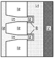
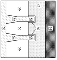
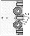
도 1은, 일부 실시예에 따른, 입체도에서의 FinFET의 예를 도시한다.
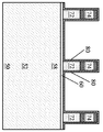
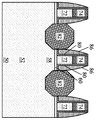
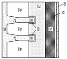
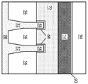
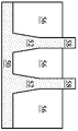
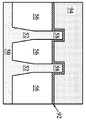
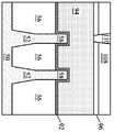
도 2, 도 3, 도 4, 도 5, 도 6, 도 7, 도 8a, 도 8b, 도 9a, 도 9b, 도 10a, 도 10b, 도 10c, 도 10d, 도 11a, 도 11b, 도 12a, 도 12b, 도 13a, 도 13b, 도 14a, 도 14b, 도 15a, 도 15b, 도 16a, 도 16b, 도 17a, 도 17b, 도 18a, 도 18b, 도 18c, 도 19a, 도 19b, 도 20a, 및 도 20b는, 일부 실시예에 따른, FinFET의 제조 중의 중간 단계의 단면도이다.
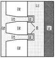
도 21a, 도 21b, 도 22a, 도 22b, 도 23a, 도 23b, 도 24a, 도 24b, 도 25a, 및 도 25b는, 일부 실시예에 따른, FinFET의 제조 중의 중간 단계의 단면도이다.
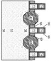
도 26a, 도 26b, 도 27a, 도 27b, 도 28a, 도 28b, 도 29a, 도 29b, 도 30a, 및 도 30b는, 일부 실시예에 따른, FinFET의 제조 중의 중간 단계의 단면도이다.
도 31a, 도 31b, 도 32a, 도 32b, 도 33a, 도 33b, 도 34a, 도 34b, 도 35a, 및 도 35b는, 일부 실시예에 따른, FinFET의 제조 중의 중간 단계의 단면도이다.
Claims (10)
- 디바이스에 있어서,
기판으로부터 연장되는 제1 핀;
상기 제1 핀 위에 있고 상기 제1 핀의 측벽을 따르는 제1 게이트 스택;
상기 제1 게이트 스택의 측벽을 따라서 배치된 제1 게이트 스페이서;
상기 제1 핀 내에 있고 상기 제1 게이트 스페이서에 인접한 제1 에피택셜 소스/드레인 영역; 및
상기 제1 에피택셜 소스/드레인 영역과 상기 제1 게이트 스페이서 사이의 보호층
을 포함하며, 상기 보호층은 상기 제1 게이트 스페이서와 상기 제1 게이트 스택 사이에 있는, 디바이스. - 제1항에 있어서, 상기 보호층은 절연층이며 상기 제1 에피택셜 소스/드레인 영역과 물리적으로 접촉하는, 디바이스.
- 제1항에 있어서, 상기 제1 게이트 스페이서는 3.5 이하의 유전 상수를 갖는, 디바이스.
- 제3항에 있어서, 상기 보호층은 제1 부분, 제2 부분, 및 제3 부분을 가지며, 상기 제1 부분은 상기 제1 게이트 스페이서의 제1 측벽을 따라서 연장되고, 상기 제2 부분은 상기 제1 게이트 스페이서의 제2 측벽을 따라서 연장되고, 상기 제1 측벽은 상기 제1 게이트 스택을 향하고, 상기 제2 측벽은 상기 제1 측벽과는 반대 방향을 향하고, 상기 보호층의 제3 부분은 상기 제1 게이트 스페이서의 하단 표면을 따라서 연장되고, 상기 제3 부분은 상기 제1 부분으로부터 상기 제2 부분까지 연장되는, 디바이스.
- 제1항에 있어서,
상기 제1 에피택셜 소스/드레인 영역 위의 에칭 정지층을 더 포함하며, 상기 보호층은 상기 에칭 정지층과 물리적으로 접촉하는, 디바이스. - 제1항에 있어서,
상기 보호층 아래에 놓이는 제1 게이트 밀봉 스페이서를 더 포함하며, 상기 제1 게이트 밀봉 스페이서는 상기 보호층과 상기 제1 게이트 스택 사이에 있는, 디바이스. - 제6항에 있어서, 상기 보호층은 SiCN으로 제조되고, 상기 제1 게이트 스페이서는 SiOCN으로 제조되며, 상기 제1 게이트 밀봉 스페이서는 SiCN으로 제조되는, 디바이스.
- 제6항에 있어서,
상기 보호층 아래에 놓이는 제1 스페이서 푸팅(footing)을 더 포함하며, 상기 제1 스페이서 푸팅은 상기 제1 게이트 밀봉 스페이서와 상기 제1 에피택셜 소스/드레인 영역 사이에 있고, 상기 보호층은 상기 제1 에피택셜 소스/드레인 영역 위에서 연장되는, 디바이스. - 방법에 있어서,
기판으로부터 위를 향해 연장되는 제1 핀 위에 그리고 상기 제1 핀의 측벽을 따라서 제1 게이트를 형성하는 단계;
상기 제1 게이트의 측벽을 따라서 제1 로우-k 게이트 스페이서를 형성하는 단계;
상기 제1 로우-k 게이트 스페이서에 인접하게 상기 제1 핀 내에 제1 리세스를 에칭하는 단계;
상기 제1 리세스 내에 제1 소스/드레인 영역을 에피택셜 성장시키는 단계;
상기 제1 로우-k 게이트 스페이서를 제거하는 단계 - 상기 제1 로우-k 게이트 스페이서를 제거하는 단계는 상기 제1 게이트와 상기 제1 소스/드레인 영역 사이에 제2 리세스를 형성함 -;
상기 제1 게이트와 상기 제1 소스/드레인 영역 위 및 상기 제2 리세스 내에 보호층을 형성하는 단계;
상기 보호층 위에 로우-k층을 형성하는 단계; 및
상기 제2 리세스 내에 제2 로우-k 게이트 스페이서를 형성하기 위해 상기 로우-k층을 에칭하는 단계 - 상기 제2 로우-k 게이트 스페이서는, 상기 제1 게이트의 측벽을 따라서 연장되는 상기 보호층을 따라서 연장됨 -
를 포함하는, 방법. - 방법에 있어서,
기판으로부터 위를 향해 연장되는 제1 핀의 위에 그리고 상기 제1 핀의 측벽을 따라서 제1 게이트를 형성하는 단계;
상기 제1 게이트의 측벽을 따라서 제1 로우-k 게이트 스페이서를 형성하는 단계;
상기 제1 로우-k 게이트 스페이서에 인접하게 상기 제1 핀 상에 제1 소스/드레인 영역을 에피택셜 성장시키는 단계;
상기 제1 로우-k 게이트 스페이서를 에칭하는 단계;
상기 제1 게이트 및 상기 제1 소스/드레인 영역 위에 유전체층을 형성하는 단계;
상기 유전체층 상에 산소 처리를 수행하는 단계; 및
상기 제1 게이트의 측벽을 따라서 제2 게이트 스페이서를 형성하기 위해, 상기 처리된 유전체층을 에칭하는 단계
를 포함하는, 방법.
Applications Claiming Priority (4)
| Application Number | Priority Date | Filing Date | Title |
|---|---|---|---|
| US201862764865P | 2018-08-16 | 2018-08-16 | |
| US62/764,865 | 2018-08-16 | ||
| US16/276,308 US11024550B2 (en) | 2018-08-16 | 2019-02-14 | Semiconductor device and method |
| US16/276,308 | 2019-02-14 |
Publications (2)
| Publication Number | Publication Date |
|---|---|
| KR20200020631A true KR20200020631A (ko) | 2020-02-26 |
| KR102302516B1 KR102302516B1 (ko) | 2021-09-17 |
Family
ID=69523005
Family Applications (1)
| Application Number | Title | Priority Date | Filing Date |
|---|---|---|---|
| KR1020190100217A Active KR102302516B1 (ko) | 2018-08-16 | 2019-08-16 | 반도체 디바이스 및 방법 |
Country Status (3)
| Country | Link |
|---|---|
| US (2) | US11024550B2 (ko) |
| KR (1) | KR102302516B1 (ko) |
| CN (1) | CN110838487B (ko) |
Cited By (7)
| Publication number | Priority date | Publication date | Assignee | Title |
|---|---|---|---|---|
| KR20210133853A (ko) * | 2020-04-28 | 2021-11-08 | 타이완 세미콘덕터 매뉴팩쳐링 컴퍼니 리미티드 | 반도체 디바이스 및 방법 |
| KR20210154681A (ko) * | 2020-06-11 | 2021-12-21 | 타이완 세미콘덕터 매뉴팩쳐링 컴퍼니 리미티드 | 반도체 디바이스 및 방법 |
| KR20220021849A (ko) * | 2020-08-14 | 2022-02-22 | 타이완 세미콘덕터 매뉴팩쳐링 컴퍼니 리미티드 | 반도체 디바이스 및 방법 |
| KR20220126612A (ko) * | 2021-03-09 | 2022-09-16 | 타이완 세미콘덕터 매뉴팩쳐링 컴퍼니 리미티드 | 도전 구조물을 갖는 반도체 구조물 및 그를 제조하기 위한 방법 |
| KR20220154603A (ko) * | 2021-05-13 | 2022-11-22 | 타이완 세미콘덕터 매뉴팩쳐링 컴퍼니 리미티드 | 트랜지스터 소스/드레인 영역 및 이를 형성하는 방법 |
| US11984402B2 (en) | 2020-04-28 | 2024-05-14 | Taiwan Semiconductor Manufacturing Co., Ltd. | Semiconductor device and method |
| US12406907B2 (en) | 2022-04-15 | 2025-09-02 | Taiwan Semiconductor Manufacturing Company, Ltd. | Semiconductor structure with conductive_structure |
Families Citing this family (12)
| Publication number | Priority date | Publication date | Assignee | Title |
|---|---|---|---|---|
| US11990548B2 (en) * | 2019-05-28 | 2024-05-21 | Etron Technology, Inc. | Transistor with low leakage currents and manufacturing method thereof |
| CN111640732B (zh) * | 2019-09-29 | 2025-01-28 | 福建省晋华集成电路有限公司 | 半导体结构及其形成方法 |
| DE102020120634A1 (de) * | 2020-01-31 | 2021-08-05 | Taiwan Semiconductor Manufacturing Co., Ltd. | Halbleitervorrichtung und verfahren |
| DE102020132620B4 (de) * | 2020-05-15 | 2026-01-29 | Taiwan Semiconductor Manufacturing Company, Ltd. | Halbleitervorrichtung und Verfahren |
| DE102020124588B4 (de) * | 2020-05-20 | 2024-11-07 | Taiwan Semiconductor Manufacturing Co., Ltd. | Prozesse zum entfernen von spitzen von gates |
| US11476347B2 (en) | 2020-05-20 | 2022-10-18 | Taiwan Semiconductor Manufacturing Co., Ltd. | Processes for removing spikes from gates |
| US11581259B2 (en) | 2020-06-25 | 2023-02-14 | Taiwan Semiconductor Manufacturing Co., Ltd. | Hybrid conductive structures |
| US11349014B2 (en) | 2020-06-30 | 2022-05-31 | Taiwan Semiconductor Manufacturing Co., Ltd. | Air spacer and method of forming same |
| CN114068704B (zh) * | 2020-07-31 | 2024-03-22 | 中芯国际集成电路制造(上海)有限公司 | 半导体结构及其形成方法 |
| US12237399B2 (en) * | 2021-08-27 | 2025-02-25 | Taiwan Semiconductor Manufacturing Co., Ltd. | Nano-FET transistor with alternating nanostructures and method of forming thereof |
| US20230128166A1 (en) * | 2021-10-26 | 2023-04-27 | Intel Corporation | Ic structures with improved bonding between a semiconductor layer and a non-semiconductor support structure |
| US20240072157A1 (en) * | 2022-08-24 | 2024-02-29 | Taiwan Semiconductor Manufacturing Company Ltd. | Semiconductor structure and forming method thereof |
Citations (6)
| Publication number | Priority date | Publication date | Assignee | Title |
|---|---|---|---|---|
| CN103383918A (zh) * | 2012-05-04 | 2013-11-06 | 联华电子股份有限公司 | 具有金属栅极的半导体结构及其制作方法 |
| KR20150061607A (ko) * | 2013-11-27 | 2015-06-04 | 타이완 세미콘덕터 매뉴팩쳐링 컴퍼니 리미티드 | 반도체 장치 및 그 제조 방법 |
| US20160099342A1 (en) * | 2014-10-02 | 2016-04-07 | International Business Machines Corporation | Structure and method to increase contact area in unmerged epi integration for cmos finfets |
| US9318367B2 (en) * | 2013-02-27 | 2016-04-19 | Taiwan Semiconductor Manufacturing Company, Ltd. | FinFET structure with different fin heights and method for forming the same |
| KR20160059861A (ko) * | 2014-11-19 | 2016-05-27 | 삼성전자주식회사 | 반도체 소자 및 이의 제조 방법 |
| KR20170061233A (ko) * | 2015-11-25 | 2017-06-05 | 삼성전자주식회사 | 반도체 소자 |
Family Cites Families (26)
| Publication number | Priority date | Publication date | Assignee | Title |
|---|---|---|---|---|
| US7642607B2 (en) * | 2005-08-10 | 2010-01-05 | Taiwan Semiconductor Manufacturing Company, Ltd. | MOS devices with reduced recess on substrate surface |
| US9245805B2 (en) | 2009-09-24 | 2016-01-26 | Taiwan Semiconductor Manufacturing Company, Ltd. | Germanium FinFETs with metal gates and stressors |
| US8450834B2 (en) | 2010-02-16 | 2013-05-28 | Taiwan Semiconductor Manufacturing Company, Ltd. | Spacer structure of a field effect transistor with an oxygen-containing layer between two oxygen-sealing layers |
| US8466502B2 (en) | 2011-03-24 | 2013-06-18 | United Microelectronics Corp. | Metal-gate CMOS device |
| US8962400B2 (en) | 2011-07-07 | 2015-02-24 | Taiwan Semiconductor Manufacturing Company, Ltd. | In-situ doping of arsenic for source and drain epitaxy |
| CN103137657B (zh) * | 2011-11-25 | 2016-08-31 | 中芯国际集成电路制造(上海)有限公司 | 半导体集成器件及其形成方法 |
| US9236267B2 (en) | 2012-02-09 | 2016-01-12 | Taiwan Semiconductor Manufacturing Company, Ltd. | Cut-mask patterning process for fin-like field effect transistor (FinFET) device |
| US9041076B2 (en) * | 2013-02-03 | 2015-05-26 | International Business Machines Corporation | Partial sacrificial dummy gate with CMOS device with high-k metal gate |
| US9159824B2 (en) | 2013-02-27 | 2015-10-13 | Taiwan Semiconductor Manufacturing Company, Ltd. | FinFETs with strained well regions |
| US9093514B2 (en) | 2013-03-06 | 2015-07-28 | Taiwan Semiconductor Manufacturing Co., Ltd. | Strained and uniform doping technique for FINFETs |
| CN104282568B (zh) * | 2013-07-06 | 2018-07-13 | 中国科学院微电子研究所 | 一种半导体结构及其制造方法 |
| US9136106B2 (en) | 2013-12-19 | 2015-09-15 | Taiwan Semiconductor Manufacturing Company, Ltd. | Method for integrated circuit patterning |
| US9608116B2 (en) | 2014-06-27 | 2017-03-28 | Taiwan Semiconductor Manufacturing Company, Ltd. | FINFETs with wrap-around silicide and method forming the same |
| US9484346B2 (en) * | 2014-10-15 | 2016-11-01 | Taiwan Semiconductor Manufacturing Company Ltd | Semiconductor structure and manufacturing method thereof |
| US9401416B2 (en) * | 2014-12-04 | 2016-07-26 | Globalfoundries Inc. | Method for reducing gate height variation due to overlapping masks |
| US9418897B1 (en) | 2015-06-15 | 2016-08-16 | Taiwan Semiconductor Manufacturing Company, Ltd. | Wrap around silicide for FinFETs |
| US9520482B1 (en) | 2015-11-13 | 2016-12-13 | Taiwan Semiconductor Manufacturing Company, Ltd. | Method of cutting metal gate |
| US9761720B2 (en) * | 2015-11-30 | 2017-09-12 | Globalfoundries Inc. | Replacement body FinFET for improved junction profile with gate self-aligned junctions |
| CN106876273B (zh) * | 2015-12-11 | 2019-12-03 | 中芯国际集成电路制造(上海)有限公司 | 半导体结构的制造方法 |
| US9685533B1 (en) | 2016-02-21 | 2017-06-20 | United Microelectronics Corp. | Transistor with SiCN/SiOCN mulitlayer spacer |
| US10008386B2 (en) * | 2016-09-12 | 2018-06-26 | International Business Machines Corporation | Formation of pure silicon oxide interfacial layer on silicon-germanium channel field effect transistor device |
| CN108122850B (zh) * | 2016-11-28 | 2020-06-09 | 中芯国际集成电路制造(上海)有限公司 | 半导体结构及其形成方法 |
| US9812363B1 (en) | 2016-11-29 | 2017-11-07 | Taiwan Semiconductor Manufacturing Company, Ltd. | FinFET device and method of forming same |
| US10079290B2 (en) | 2016-12-30 | 2018-09-18 | United Microelectronics Corp. | Semiconductor device having asymmetric spacer structures |
| US10395991B2 (en) * | 2017-12-04 | 2019-08-27 | United Microelectronics Corp. | Semiconductor device and method for fabricating the same |
| US10790148B2 (en) * | 2018-05-23 | 2020-09-29 | Globalfoundries Inc. | Method to increase effective gate height |
-
2019
- 2019-02-14 US US16/276,308 patent/US11024550B2/en active Active
- 2019-07-29 CN CN201910689499.4A patent/CN110838487B/zh active Active
- 2019-08-16 KR KR1020190100217A patent/KR102302516B1/ko active Active
-
2021
- 2021-05-28 US US17/333,116 patent/US11908750B2/en active Active
Patent Citations (6)
| Publication number | Priority date | Publication date | Assignee | Title |
|---|---|---|---|---|
| CN103383918A (zh) * | 2012-05-04 | 2013-11-06 | 联华电子股份有限公司 | 具有金属栅极的半导体结构及其制作方法 |
| US9318367B2 (en) * | 2013-02-27 | 2016-04-19 | Taiwan Semiconductor Manufacturing Company, Ltd. | FinFET structure with different fin heights and method for forming the same |
| KR20150061607A (ko) * | 2013-11-27 | 2015-06-04 | 타이완 세미콘덕터 매뉴팩쳐링 컴퍼니 리미티드 | 반도체 장치 및 그 제조 방법 |
| US20160099342A1 (en) * | 2014-10-02 | 2016-04-07 | International Business Machines Corporation | Structure and method to increase contact area in unmerged epi integration for cmos finfets |
| KR20160059861A (ko) * | 2014-11-19 | 2016-05-27 | 삼성전자주식회사 | 반도체 소자 및 이의 제조 방법 |
| KR20170061233A (ko) * | 2015-11-25 | 2017-06-05 | 삼성전자주식회사 | 반도체 소자 |
Cited By (14)
| Publication number | Priority date | Publication date | Assignee | Title |
|---|---|---|---|---|
| US12374624B2 (en) | 2020-04-28 | 2025-07-29 | Taiwan Semiconductor Manufacturing Co., Ltd. | Semiconductor devices |
| US11410930B2 (en) | 2020-04-28 | 2022-08-09 | Taiwan Semiconductor Manufacturing Co., Ltd. | Semiconductor device and method |
| US11984402B2 (en) | 2020-04-28 | 2024-05-14 | Taiwan Semiconductor Manufacturing Co., Ltd. | Semiconductor device and method |
| KR20210133853A (ko) * | 2020-04-28 | 2021-11-08 | 타이완 세미콘덕터 매뉴팩쳐링 컴퍼니 리미티드 | 반도체 디바이스 및 방법 |
| KR20210154681A (ko) * | 2020-06-11 | 2021-12-21 | 타이완 세미콘덕터 매뉴팩쳐링 컴퍼니 리미티드 | 반도체 디바이스 및 방법 |
| US12119231B2 (en) | 2020-06-11 | 2024-10-15 | Taiwan Semiconductor Manufacturing Co., Ltd. | Semiconductor device and method |
| KR20220021849A (ko) * | 2020-08-14 | 2022-02-22 | 타이완 세미콘덕터 매뉴팩쳐링 컴퍼니 리미티드 | 반도체 디바이스 및 방법 |
| US12453118B2 (en) | 2020-08-14 | 2025-10-21 | Taiwan Semiconductor Manufacturing Co., Ltd. | Inter-layer dielectrics and etch stop layers for transistor source/drain regions |
| US12389646B2 (en) | 2021-03-09 | 2025-08-12 | Taiwan Semiconductor Manufacturing Company, Ltd. | Semiconductor transistor structure with nanostructures and conductive structure and method for manufacturing the same |
| US11961886B2 (en) | 2021-03-09 | 2024-04-16 | Taiwan Semiconductor Manufacturing Company, Ltd. | Semiconductor structure with conductive structure |
| KR20220126612A (ko) * | 2021-03-09 | 2022-09-16 | 타이완 세미콘덕터 매뉴팩쳐링 컴퍼니 리미티드 | 도전 구조물을 갖는 반도체 구조물 및 그를 제조하기 위한 방법 |
| US12419084B2 (en) | 2021-05-13 | 2025-09-16 | Taiwan Semiconductor Manufacturing Co., Ltd. | Methods of forming transistor source/drain regions comprising carbon liner layers |
| KR20220154603A (ko) * | 2021-05-13 | 2022-11-22 | 타이완 세미콘덕터 매뉴팩쳐링 컴퍼니 리미티드 | 트랜지스터 소스/드레인 영역 및 이를 형성하는 방법 |
| US12406907B2 (en) | 2022-04-15 | 2025-09-02 | Taiwan Semiconductor Manufacturing Company, Ltd. | Semiconductor structure with conductive_structure |
Also Published As
| Publication number | Publication date |
|---|---|
| US11908750B2 (en) | 2024-02-20 |
| CN110838487B (zh) | 2022-09-30 |
| CN110838487A (zh) | 2020-02-25 |
| US11024550B2 (en) | 2021-06-01 |
| US20210287948A1 (en) | 2021-09-16 |
| KR102302516B1 (ko) | 2021-09-17 |
| US20200058561A1 (en) | 2020-02-20 |
Similar Documents
| Publication | Publication Date | Title |
|---|---|---|
| KR102302516B1 (ko) | 반도체 디바이스 및 방법 | |
| US12068389B2 (en) | Semiconductor device including gas spacers and method of manufacture | |
| US11315837B2 (en) | Semiconductor device and method | |
| US12142668B2 (en) | Semiconductor device and method | |
| US11532507B2 (en) | Semiconductor device and method | |
| US11594618B2 (en) | FinFET devices and methods of forming | |
| US12610609B2 (en) | Method of forming FinFET with protected low-k gate spacers | |
| KR102284473B1 (ko) | 반도체 디바이스 및 방법 | |
| TWI739147B (zh) | 半導體裝置及其形成方法 | |
| KR20220160469A (ko) | 반도체 디바이스 상의 유전체층 및 그 형성방법 | |
| US11056573B2 (en) | Implantation and annealing for semiconductor device | |
| KR102549844B1 (ko) | 반도체 디바이스 및 방법 | |
| TWI787817B (zh) | 半導體元件的製造方法 |
Legal Events
| Date | Code | Title | Description |
|---|---|---|---|
| A201 | Request for examination | ||
| PA0109 | Patent application |
St.27 status event code: A-0-1-A10-A12-nap-PA0109 |
|
| PA0201 | Request for examination |
St.27 status event code: A-1-2-D10-D11-exm-PA0201 |
|
| R18-X000 | Changes to party contact information recorded |
St.27 status event code: A-3-3-R10-R18-oth-X000 |
|
| D13-X000 | Search requested |
St.27 status event code: A-1-2-D10-D13-srh-X000 |
|
| PG1501 | Laying open of application |
St.27 status event code: A-1-1-Q10-Q12-nap-PG1501 |
|
| D14-X000 | Search report completed |
St.27 status event code: A-1-2-D10-D14-srh-X000 |
|
| E902 | Notification of reason for refusal | ||
| PE0902 | Notice of grounds for rejection |
St.27 status event code: A-1-2-D10-D21-exm-PE0902 |
|
| T11-X000 | Administrative time limit extension requested |
St.27 status event code: U-3-3-T10-T11-oth-X000 |
|
| T11-X000 | Administrative time limit extension requested |
St.27 status event code: U-3-3-T10-T11-oth-X000 |
|
| T11-X000 | Administrative time limit extension requested |
St.27 status event code: U-3-3-T10-T11-oth-X000 |
|
| T11-X000 | Administrative time limit extension requested |
St.27 status event code: U-3-3-T10-T11-oth-X000 |
|
| E13-X000 | Pre-grant limitation requested |
St.27 status event code: A-2-3-E10-E13-lim-X000 |
|
| P11-X000 | Amendment of application requested |
St.27 status event code: A-2-2-P10-P11-nap-X000 |
|
| P13-X000 | Application amended |
St.27 status event code: A-2-2-P10-P13-nap-X000 |
|
| E701 | Decision to grant or registration of patent right | ||
| PE0701 | Decision of registration |
St.27 status event code: A-1-2-D10-D22-exm-PE0701 |
|
| GRNT | Written decision to grant | ||
| PR0701 | Registration of establishment |
St.27 status event code: A-2-4-F10-F11-exm-PR0701 |
|
| PR1002 | Payment of registration fee |
St.27 status event code: A-2-2-U10-U11-oth-PR1002 Fee payment year number: 1 |
|
| PG1601 | Publication of registration |
St.27 status event code: A-4-4-Q10-Q13-nap-PG1601 |
|
| PR1001 | Payment of annual fee |
St.27 status event code: A-4-4-U10-U11-oth-PR1001 Fee payment year number: 4 |
|
| P22-X000 | Classification modified |
St.27 status event code: A-4-4-P10-P22-nap-X000 |
|
| P22-X000 | Classification modified |
St.27 status event code: A-4-4-P10-P22-nap-X000 |