KR20200020962A - 듀얼 포지션 마그네트론 및 중앙에서 공급되는 냉각제를 갖는 캐소드 조립체 - Google Patents
듀얼 포지션 마그네트론 및 중앙에서 공급되는 냉각제를 갖는 캐소드 조립체 Download PDFInfo
- Publication number
- KR20200020962A KR20200020962A KR1020207004188A KR20207004188A KR20200020962A KR 20200020962 A KR20200020962 A KR 20200020962A KR 1020207004188 A KR1020207004188 A KR 1020207004188A KR 20207004188 A KR20207004188 A KR 20207004188A KR 20200020962 A KR20200020962 A KR 20200020962A
- Authority
- KR
- South Korea
- Prior art keywords
- assembly
- target
- rotatable magnet
- magnetron
- central axis
- Prior art date
- Legal status (The legal status is an assumption and is not a legal conclusion. Google has not performed a legal analysis and makes no representation as to the accuracy of the status listed.)
- Granted
Links
Images

Classifications
-
- H—ELECTRICITY
- H01—ELECTRIC ELEMENTS
- H01J—ELECTRIC DISCHARGE TUBES OR DISCHARGE LAMPS
- H01J37/00—Discharge tubes with provision for introducing objects or material to be exposed to the discharge, e.g. for the purpose of examination or processing thereof
- H01J37/32—Gas-filled discharge tubes
- H01J37/34—Gas-filled discharge tubes operating with cathodic sputtering
- H01J37/3411—Constructional aspects of the reactor
- H01J37/345—Magnet arrangements in particular for cathodic sputtering apparatus
- H01J37/3455—Movable magnets
-
- C—CHEMISTRY; METALLURGY
- C23—COATING METALLIC MATERIAL; COATING MATERIAL WITH METALLIC MATERIAL; CHEMICAL SURFACE TREATMENT; DIFFUSION TREATMENT OF METALLIC MATERIAL; COATING BY VACUUM EVAPORATION, BY SPUTTERING, BY ION IMPLANTATION OR BY CHEMICAL VAPOUR DEPOSITION, IN GENERAL; INHIBITING CORROSION OF METALLIC MATERIAL OR INCRUSTATION IN GENERAL
- C23C—COATING METALLIC MATERIAL; COATING MATERIAL WITH METALLIC MATERIAL; SURFACE TREATMENT OF METALLIC MATERIAL BY DIFFUSION INTO THE SURFACE, BY CHEMICAL CONVERSION OR SUBSTITUTION; COATING BY VACUUM EVAPORATION, BY SPUTTERING, BY ION IMPLANTATION OR BY CHEMICAL VAPOUR DEPOSITION, IN GENERAL
- C23C14/00—Coating by vacuum evaporation, by sputtering or by ion implantation of the coating forming material
- C23C14/22—Coating by vacuum evaporation, by sputtering or by ion implantation of the coating forming material characterised by the process of coating
- C23C14/34—Sputtering
- C23C14/3407—Cathode assembly for sputtering apparatus, e.g. Target
-
- C—CHEMISTRY; METALLURGY
- C23—COATING METALLIC MATERIAL; COATING MATERIAL WITH METALLIC MATERIAL; CHEMICAL SURFACE TREATMENT; DIFFUSION TREATMENT OF METALLIC MATERIAL; COATING BY VACUUM EVAPORATION, BY SPUTTERING, BY ION IMPLANTATION OR BY CHEMICAL VAPOUR DEPOSITION, IN GENERAL; INHIBITING CORROSION OF METALLIC MATERIAL OR INCRUSTATION IN GENERAL
- C23C—COATING METALLIC MATERIAL; COATING MATERIAL WITH METALLIC MATERIAL; SURFACE TREATMENT OF METALLIC MATERIAL BY DIFFUSION INTO THE SURFACE, BY CHEMICAL CONVERSION OR SUBSTITUTION; COATING BY VACUUM EVAPORATION, BY SPUTTERING, BY ION IMPLANTATION OR BY CHEMICAL VAPOUR DEPOSITION, IN GENERAL
- C23C14/00—Coating by vacuum evaporation, by sputtering or by ion implantation of the coating forming material
- C23C14/22—Coating by vacuum evaporation, by sputtering or by ion implantation of the coating forming material characterised by the process of coating
- C23C14/34—Sputtering
- C23C14/3435—Applying energy to the substrate during sputtering
- C23C14/345—Applying energy to the substrate during sputtering using substrate bias
-
- C—CHEMISTRY; METALLURGY
- C23—COATING METALLIC MATERIAL; COATING MATERIAL WITH METALLIC MATERIAL; CHEMICAL SURFACE TREATMENT; DIFFUSION TREATMENT OF METALLIC MATERIAL; COATING BY VACUUM EVAPORATION, BY SPUTTERING, BY ION IMPLANTATION OR BY CHEMICAL VAPOUR DEPOSITION, IN GENERAL; INHIBITING CORROSION OF METALLIC MATERIAL OR INCRUSTATION IN GENERAL
- C23C—COATING METALLIC MATERIAL; COATING MATERIAL WITH METALLIC MATERIAL; SURFACE TREATMENT OF METALLIC MATERIAL BY DIFFUSION INTO THE SURFACE, BY CHEMICAL CONVERSION OR SUBSTITUTION; COATING BY VACUUM EVAPORATION, BY SPUTTERING, BY ION IMPLANTATION OR BY CHEMICAL VAPOUR DEPOSITION, IN GENERAL
- C23C14/00—Coating by vacuum evaporation, by sputtering or by ion implantation of the coating forming material
- C23C14/22—Coating by vacuum evaporation, by sputtering or by ion implantation of the coating forming material characterised by the process of coating
- C23C14/34—Sputtering
- C23C14/35—Sputtering by application of a magnetic field, e.g. magnetron sputtering
-
- H—ELECTRICITY
- H01—ELECTRIC ELEMENTS
- H01J—ELECTRIC DISCHARGE TUBES OR DISCHARGE LAMPS
- H01J37/00—Discharge tubes with provision for introducing objects or material to be exposed to the discharge, e.g. for the purpose of examination or processing thereof
- H01J37/32—Gas-filled discharge tubes
- H01J37/34—Gas-filled discharge tubes operating with cathodic sputtering
- H01J37/3402—Gas-filled discharge tubes operating with cathodic sputtering using supplementary magnetic fields
- H01J37/3405—Magnetron sputtering
-
- H—ELECTRICITY
- H01—ELECTRIC ELEMENTS
- H01J—ELECTRIC DISCHARGE TUBES OR DISCHARGE LAMPS
- H01J37/00—Discharge tubes with provision for introducing objects or material to be exposed to the discharge, e.g. for the purpose of examination or processing thereof
- H01J37/32—Gas-filled discharge tubes
- H01J37/34—Gas-filled discharge tubes operating with cathodic sputtering
- H01J37/3402—Gas-filled discharge tubes operating with cathodic sputtering using supplementary magnetic fields
- H01J37/3405—Magnetron sputtering
- H01J37/3408—Planar magnetron sputtering
-
- H—ELECTRICITY
- H01—ELECTRIC ELEMENTS
- H01J—ELECTRIC DISCHARGE TUBES OR DISCHARGE LAMPS
- H01J37/00—Discharge tubes with provision for introducing objects or material to be exposed to the discharge, e.g. for the purpose of examination or processing thereof
- H01J37/32—Gas-filled discharge tubes
- H01J37/34—Gas-filled discharge tubes operating with cathodic sputtering
- H01J37/3411—Constructional aspects of the reactor
- H01J37/3414—Targets
- H01J37/3426—Material
-
- H—ELECTRICITY
- H01—ELECTRIC ELEMENTS
- H01J—ELECTRIC DISCHARGE TUBES OR DISCHARGE LAMPS
- H01J37/00—Discharge tubes with provision for introducing objects or material to be exposed to the discharge, e.g. for the purpose of examination or processing thereof
- H01J37/32—Gas-filled discharge tubes
- H01J37/34—Gas-filled discharge tubes operating with cathodic sputtering
- H01J37/3411—Constructional aspects of the reactor
- H01J37/3435—Target holders (includes backing plates and endblocks)
-
- H—ELECTRICITY
- H01—ELECTRIC ELEMENTS
- H01J—ELECTRIC DISCHARGE TUBES OR DISCHARGE LAMPS
- H01J37/00—Discharge tubes with provision for introducing objects or material to be exposed to the discharge, e.g. for the purpose of examination or processing thereof
- H01J37/32—Gas-filled discharge tubes
- H01J37/34—Gas-filled discharge tubes operating with cathodic sputtering
- H01J37/3464—Operating strategies
- H01J37/347—Thickness uniformity of coated layers or desired profile of target erosion
-
- H—ELECTRICITY
- H01—ELECTRIC ELEMENTS
- H01J—ELECTRIC DISCHARGE TUBES OR DISCHARGE LAMPS
- H01J37/00—Discharge tubes with provision for introducing objects or material to be exposed to the discharge, e.g. for the purpose of examination or processing thereof
- H01J37/32—Gas-filled discharge tubes
- H01J37/34—Gas-filled discharge tubes operating with cathodic sputtering
- H01J37/3488—Constructional details of particle beam apparatus not otherwise provided for, e.g. arrangement, mounting, housing, environment; special provisions for cleaning or maintenance of the apparatus
- H01J37/3497—Temperature of target
Landscapes
- Chemical & Material Sciences (AREA)
- Engineering & Computer Science (AREA)
- Physics & Mathematics (AREA)
- Plasma & Fusion (AREA)
- Analytical Chemistry (AREA)
- Materials Engineering (AREA)
- Chemical Kinetics & Catalysis (AREA)
- Mechanical Engineering (AREA)
- Metallurgy (AREA)
- Organic Chemistry (AREA)
- Physical Vapour Deposition (AREA)
- Internal Circuitry In Semiconductor Integrated Circuit Devices (AREA)
- Control Of High-Frequency Heating Circuits (AREA)
- Constitution Of High-Frequency Heating (AREA)
Abstract
Description
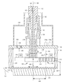
[0012] 도 1은 본 개시내용의 일부 실시예들에 따른 프로세스 챔버의 개략적인 단면도를 도시한다.
[0013] 도 2는 본 개시내용의 일부 실시예들에 따른 마그네트론 조립체의 개략적인 단면도를 도시한다.
[0014] 이해를 용이하게 하기 위해, 도면들에 대해 공통인 동일한 엘리먼트들을 지정하기 위해 가능한 경우 동일한 참조 번호들이 사용되었다. 도면들은 실척대로 도시된 것이 아니고, 명확성을 위해 간략화될 수 있다. 일 실시예의 엘리먼트들 및 특징들은 추가적인 설명 없이 다른 실시예들에 유익하게 포함될 수 있다.
Claims (15)
- 마그네트론 조립체로서,
상기 마그네트론 조립체의 중심 축을 따라 연장되는 바디(body);
냉각제 피드 구조(coolant feed structure) ― 상기 냉각제 피드 구조는, 상기 중심 축을 따라 상기 냉각제 피드 구조 아래의 영역에 냉각제를 제공하기 위해, 상기 중심 축을 따라 상기 바디를 통해 연장됨 ―; 및
상기 바디의 최하부에 커플링되고, 복수의 자석들을 갖는 회전가능 자석 조립체
를 포함하며,
상기 회전가능 자석 조립체는 수직으로 이동하도록 구성되는,
마그네트론 조립체. - 제1 항에 있어서,
상기 회전가능 자석 조립체는, 상기 중심 축으로부터의 제1 거리 및 상기 중심 축으로부터의 제2 거리에서, 상기 중심 축을 중심으로 회전하도록 구성되는,
마그네트론 조립체. - 제2 항에 있어서,
상기 회전가능 자석 조립체가 상기 제1 거리에서 회전하고 있을 때를 검출하도록 구성된 제1 센서; 및
상기 회전가능 자석 조립체가 상기 제2 거리에서 회전하고 있을 때를 검출하도록 구성된 제2 센서
를 더 포함하는,
마그네트론 조립체. - 제3 항에 있어서,
상기 회전가능 자석 조립체는,
상기 복수의 자석들이 상기 제1 거리에서 회전되고 있는지 또는 상기 제2 거리에서 회전되고 있는지를 결정하기 위해, 상기 제1 센서 및 상기 제2 센서에 의해 검출가능한 표시 엘리먼트를 더 포함하는,
마그네트론 조립체. - 제1 항 내지 제4 항 중 어느 한 항에 있어서,
상기 회전가능 자석 조립체가 회전하고 있는지를 결정하고, 상기 회전가능 자석 조립체의 수직 포지션을 결정하도록 구성된 제3 센서를 더 포함하는,
마그네트론 조립체. - 제1 항 내지 제4 항 중 어느 한 항에 있어서,
상기 복수의 자석들은 상기 복수의 자석들의 중앙을 통과하는 자석 축을 중심으로 회전하도록 구성되는,
마그네트론 조립체. - 제1 항 내지 제4 항 중 어느 한 항에 있어서,
상기 회전가능 자석 조립체의 수직 포지션을 제어하기 위해 상기 바디에 커플링된 모터를 더 포함하는,
마그네트론 조립체. - 제1 항 내지 제4 항 중 어느 한 항에 있어서,
상기 바디는 텔레스코핑 바디(telescoping body)인,
마그네트론 조립체. - 기판 프로세싱 시스템으로서,
챔버;
상기 챔버의 최상부에 제거가능하게 배치된 덮개;
상기 덮개에 커플링된 타겟 조립체 ― 상기 타겟 조립체는 상기 타겟 조립체로부터 스퍼터링되어 기판 상에 증착될 타겟 재료를 포함함 ―;
프로세싱 동안 기판을 지지하기 위해 상기 챔버 내에 배치된 기판 지지부;
냉각제 공급부; 및
상기 타겟 조립체 근방에서 상기 기판 지지부와 대향하는 측에 배치된, 제1 항 내지 제4 항 중 어느 한 항에 기재된 마그네트론 조립체
를 포함하며,
상기 냉각제 피드 구조는, 상기 타겟 조립체를 냉각시키기 위해, 상기 냉각제 공급부로부터 상기 중심 축을 따라 상기 타겟 조립체 위의 공동으로 상기 냉각제를 제공하도록 구성되고,
상기 회전가능 자석 조립체는 상기 공동에 배치되는,
기판 프로세싱 시스템. - 제9 항에 있어서,
상기 바디 및 상기 회전가능 자석 조립체를 회전시키기 위해, 커플링 조립체를 통해 상기 바디에 커플링된 제1 모터; 및
상기 공동 내에서 상기 회전가능 자석 조립체를 수직으로 이동시키기 위해, 상기 바디에 커플링된 제2 모터
를 더 포함하는,
기판 프로세싱 시스템. - 제10 항에 있어서,
상기 제2 모터는, 상기 복수의 자석들의 제1 최하측 표면과 상기 타겟 조립체의 제2 최하측 표면 사이의 수직 거리가 실질적으로 일정하게 유지되도록, 상기 회전가능 자석 조립체를 수직으로 이동시키도록 구성되는,
기판 프로세싱 시스템. - 제9 항에 있어서,
상기 냉각제 피드 구조는 상기 타겟 조립체를 약 200 ℃ 미만의 온도로 유지하도록 구성되는,
기판 프로세싱 시스템. - 제9 항에 있어서,
상기 타겟 조립체에 커플링된 DC 전력 소스; 및
상기 타겟 조립체에 커플링된 RF 전력 소스
를 더 포함하는,
기판 프로세싱 시스템. - 제9 항에 있어서,
상기 타겟 재료는, 티타늄, 탄탈럼, 또는 텅스텐 중 하나를 포함하는,
기판 프로세싱 시스템. - 제9 항에 있어서,
상기 바디는 텔레스코핑 바디인,
기판 프로세싱 시스템.
Applications Claiming Priority (3)
| Application Number | Priority Date | Filing Date | Title |
|---|---|---|---|
| US15/651,791 | 2017-07-17 | ||
| US15/651,791 US11189472B2 (en) | 2017-07-17 | 2017-07-17 | Cathode assembly having a dual position magnetron and centrally fed coolant |
| PCT/US2018/042280 WO2019018283A1 (en) | 2017-07-17 | 2018-07-16 | CATHODE ASSEMBLY HAVING A DOUBLE POSITION MAGNETRON AND A CENTRALLY SUPPLY COOLING AGENT |
Publications (2)
| Publication Number | Publication Date |
|---|---|
| KR20200020962A true KR20200020962A (ko) | 2020-02-26 |
| KR102605911B1 KR102605911B1 (ko) | 2023-11-23 |
Family
ID=64999200
Family Applications (1)
| Application Number | Title | Priority Date | Filing Date |
|---|---|---|---|
| KR1020207004188A Active KR102605911B1 (ko) | 2017-07-17 | 2018-07-16 | 듀얼 포지션 마그네트론 및 중앙에서 공급되는 냉각제를 갖는 캐소드 조립체 |
Country Status (8)
| Country | Link |
|---|---|
| US (1) | US11189472B2 (ko) |
| EP (1) | EP3655986B1 (ko) |
| JP (1) | JP7354090B2 (ko) |
| KR (1) | KR102605911B1 (ko) |
| CN (1) | CN111033683B (ko) |
| SG (1) | SG11202000190XA (ko) |
| TW (1) | TWI795420B (ko) |
| WO (1) | WO2019018283A1 (ko) |
Families Citing this family (3)
| Publication number | Priority date | Publication date | Assignee | Title |
|---|---|---|---|---|
| US11024490B2 (en) | 2017-12-11 | 2021-06-01 | Applied Materials, Inc. | Magnetron having enhanced target cooling configuration |
| CN116783324B (zh) * | 2021-05-21 | 2025-11-28 | 株式会社爱发科 | 磁控溅射装置用阴极单元及磁控溅射装置 |
| US11469080B1 (en) | 2021-05-24 | 2022-10-11 | Applied Materials, Inc. | Magnetron assembly having coolant guide for enhanced target cooling |
Citations (4)
| Publication number | Priority date | Publication date | Assignee | Title |
|---|---|---|---|---|
| US20040050690A1 (en) * | 2000-12-05 | 2004-03-18 | Green Gordon Robert | Magnetron sputtering apparatus |
| US20050133361A1 (en) * | 2003-12-12 | 2005-06-23 | Applied Materials, Inc. | Compensation of spacing between magnetron and sputter target |
| US20100243440A1 (en) * | 2004-03-24 | 2010-09-30 | Applied Materials, Incorporated | Mechanism for continuously varying radial position of a magnetron |
| US20140246314A1 (en) * | 2013-03-01 | 2014-09-04 | Applied Materials, Inc. | Configurable variable position closed track magnetron |
Family Cites Families (21)
| Publication number | Priority date | Publication date | Assignee | Title |
|---|---|---|---|---|
| FR2627008B1 (fr) | 1988-02-05 | 1990-06-08 | Europ Composants Electron | Procede d'impregnation de condensateurs electrolytiques par des sels de tetracyanoquinodimethane |
| JPH02175866A (ja) * | 1988-12-27 | 1990-07-09 | Mitsumi Electric Co Ltd | 薄膜の製造方法及びその製造装置 |
| JPH10251849A (ja) | 1997-03-07 | 1998-09-22 | Tadahiro Omi | スパッタリング装置 |
| US6641701B1 (en) | 2000-06-14 | 2003-11-04 | Applied Materials, Inc. | Cooling system for magnetron sputtering apparatus |
| DE10039943A1 (de) * | 2000-08-16 | 2002-02-28 | Adc Automotive Dist Control | Verfahren zum Betreiben eines Radarsystems |
| AU2002308295B2 (en) * | 2001-03-12 | 2007-08-23 | Intercept Pharmaceuticals, Inc. | Steroids as agonists for FXR |
| JP2003147522A (ja) * | 2001-11-13 | 2003-05-21 | Seiko Epson Corp | マグネトロンスパッタ装置 |
| US7392880B2 (en) * | 2002-04-02 | 2008-07-01 | Gibson Guitar Corp. | Dual range horn with acoustic crossover |
| US6852202B2 (en) * | 2002-05-21 | 2005-02-08 | Applied Materials, Inc. | Small epicyclic magnetron with controlled radial sputtering profile |
| US6928095B2 (en) * | 2003-07-18 | 2005-08-09 | Eastman Kodak Company | Organic vertical cavity laser array device with varying pixel sizes |
| US8597479B2 (en) * | 2005-02-08 | 2013-12-03 | Tohoku Seiki Industries, Ltd. | Sputtering system |
| US8021527B2 (en) * | 2005-09-14 | 2011-09-20 | Applied Materials, Inc. | Coaxial shafts for radial positioning of rotating magnetron |
| US20100024340A1 (en) * | 2006-03-03 | 2010-02-04 | Block Shields Llc | Wind blocking device for buildings |
| CN101506446A (zh) * | 2006-08-24 | 2009-08-12 | 冈部株式会社 | 钢筋接合件 |
| US8114256B2 (en) * | 2007-11-30 | 2012-02-14 | Applied Materials, Inc. | Control of arbitrary scan path of a rotating magnetron |
| US8992741B2 (en) * | 2008-08-08 | 2015-03-31 | Applied Materials, Inc. | Method for ultra-uniform sputter deposition using simultaneous RF and DC power on target |
| JP2012140648A (ja) * | 2010-12-28 | 2012-07-26 | Canon Anelva Corp | スパッタリング装置及びそのスパッタリング方法 |
| US9096927B2 (en) | 2011-09-02 | 2015-08-04 | Applied Materials, Inc. | Cooling ring for physical vapor deposition chamber target |
| US9093252B2 (en) * | 2012-02-16 | 2015-07-28 | Taiwan Semiconductor Manufacturing Co., Ltd. | Rotation plus vibration magnet for magnetron sputtering apparatus |
| US20140061039A1 (en) | 2012-09-05 | 2014-03-06 | Applied Materials, Inc. | Target cooling for physical vapor deposition (pvd) processing systems |
| US9249500B2 (en) * | 2013-02-07 | 2016-02-02 | Applied Materials, Inc. | PVD RF DC open/closed loop selectable magnetron |
-
2017
- 2017-07-17 US US15/651,791 patent/US11189472B2/en active Active
-
2018
- 2018-07-16 KR KR1020207004188A patent/KR102605911B1/ko active Active
- 2018-07-16 JP JP2020502391A patent/JP7354090B2/ja active Active
- 2018-07-16 WO PCT/US2018/042280 patent/WO2019018283A1/en not_active Ceased
- 2018-07-16 CN CN201880046250.5A patent/CN111033683B/zh active Active
- 2018-07-16 SG SG11202000190XA patent/SG11202000190XA/en unknown
- 2018-07-16 EP EP18834519.3A patent/EP3655986B1/en active Active
- 2018-07-17 TW TW107124630A patent/TWI795420B/zh active
Patent Citations (4)
| Publication number | Priority date | Publication date | Assignee | Title |
|---|---|---|---|---|
| US20040050690A1 (en) * | 2000-12-05 | 2004-03-18 | Green Gordon Robert | Magnetron sputtering apparatus |
| US20050133361A1 (en) * | 2003-12-12 | 2005-06-23 | Applied Materials, Inc. | Compensation of spacing between magnetron and sputter target |
| US20100243440A1 (en) * | 2004-03-24 | 2010-09-30 | Applied Materials, Incorporated | Mechanism for continuously varying radial position of a magnetron |
| US20140246314A1 (en) * | 2013-03-01 | 2014-09-04 | Applied Materials, Inc. | Configurable variable position closed track magnetron |
Also Published As
| Publication number | Publication date |
|---|---|
| KR102605911B1 (ko) | 2023-11-23 |
| WO2019018283A1 (en) | 2019-01-24 |
| CN111033683A (zh) | 2020-04-17 |
| EP3655986A1 (en) | 2020-05-27 |
| TWI795420B (zh) | 2023-03-11 |
| CN111033683B (zh) | 2023-04-18 |
| JP7354090B2 (ja) | 2023-10-02 |
| EP3655986B1 (en) | 2023-05-03 |
| SG11202000190XA (en) | 2020-02-27 |
| US11189472B2 (en) | 2021-11-30 |
| EP3655986A4 (en) | 2021-04-14 |
| JP2020527652A (ja) | 2020-09-10 |
| US20190019658A1 (en) | 2019-01-17 |
| TW201908505A (zh) | 2019-03-01 |
Similar Documents
| Publication | Publication Date | Title |
|---|---|---|
| US9249500B2 (en) | PVD RF DC open/closed loop selectable magnetron | |
| US9957601B2 (en) | Apparatus for gas injection in a physical vapor deposition chamber | |
| US8647485B2 (en) | Process kit shield for plasma enhanced processing chamber | |
| US9177763B2 (en) | Method and apparatus for measuring pressure in a physical vapor deposition chamber | |
| KR102131218B1 (ko) | 플라즈마제한 갭을 갖는 프로세스 키트 | |
| KR20170044188A (ko) | 타겟 수명에 걸쳐서 낮은 불-균일성을 유지하기 위한 방법들 및 장치 | |
| KR102605911B1 (ko) | 듀얼 포지션 마그네트론 및 중앙에서 공급되는 냉각제를 갖는 캐소드 조립체 | |
| US9255322B2 (en) | Substrate processing system having symmetric RF distribution and return paths | |
| US11024490B2 (en) | Magnetron having enhanced target cooling configuration | |
| KR20170067882A (ko) | 키트 수명을 개선하기 위한 고 압축 응력 막 증착을 위한 장치 | |
| US11469080B1 (en) | Magnetron assembly having coolant guide for enhanced target cooling | |
| KR102901339B1 (ko) | Pvd(physical vapor deposition)를 위한 다중-반경 마그네트론 및 그 사용 방법들 |
Legal Events
| Date | Code | Title | Description |
|---|---|---|---|
| PA0105 | International application |
St.27 status event code: A-0-1-A10-A15-nap-PA0105 |
|
| PG1501 | Laying open of application |
St.27 status event code: A-1-1-Q10-Q12-nap-PG1501 |
|
| A201 | Request for examination | ||
| PA0201 | Request for examination |
St.27 status event code: A-1-2-D10-D11-exm-PA0201 |
|
| E902 | Notification of reason for refusal | ||
| PE0902 | Notice of grounds for rejection |
St.27 status event code: A-1-2-D10-D21-exm-PE0902 |
|
| E13-X000 | Pre-grant limitation requested |
St.27 status event code: A-2-3-E10-E13-lim-X000 |
|
| P11-X000 | Amendment of application requested |
St.27 status event code: A-2-2-P10-P11-nap-X000 |
|
| P13-X000 | Application amended |
St.27 status event code: A-2-2-P10-P13-nap-X000 |
|
| E701 | Decision to grant or registration of patent right | ||
| PE0701 | Decision of registration |
St.27 status event code: A-1-2-D10-D22-exm-PE0701 |
|
| GRNT | Written decision to grant | ||
| PR0701 | Registration of establishment |
St.27 status event code: A-2-4-F10-F11-exm-PR0701 |
|
| PR1002 | Payment of registration fee |
St.27 status event code: A-2-2-U10-U12-oth-PR1002 Fee payment year number: 1 |
|
| PG1601 | Publication of registration |
St.27 status event code: A-4-4-Q10-Q13-nap-PG1601 |
|
| R17 | Change to representative recorded |
Free format text: ST27 STATUS EVENT CODE: A-5-5-R10-R17-OTH-X000 (AS PROVIDED BY THE NATIONAL OFFICE) |
|
| R17-X000 | Change to representative recorded |
St.27 status event code: A-5-5-R10-R17-oth-X000 |