KR20200021539A - 제1 물체를 제2 물체에 대하여 위치 결정하는 장치 및 방법 - Google Patents
제1 물체를 제2 물체에 대하여 위치 결정하는 장치 및 방법 Download PDFInfo
- Publication number
- KR20200021539A KR20200021539A KR1020207003992A KR20207003992A KR20200021539A KR 20200021539 A KR20200021539 A KR 20200021539A KR 1020207003992 A KR1020207003992 A KR 1020207003992A KR 20207003992 A KR20207003992 A KR 20207003992A KR 20200021539 A KR20200021539 A KR 20200021539A
- Authority
- KR
- South Korea
- Prior art keywords
- scale
- bonding
- specifying means
- moving
- movable body
- Prior art date
- Legal status (The legal status is an assumption and is not a legal conclusion. Google has not performed a legal analysis and makes no representation as to the accuracy of the status listed.)
- Granted
Links
Images


Classifications
-
- H—ELECTRICITY
- H10—SEMICONDUCTOR DEVICES; ELECTRIC SOLID-STATE DEVICES NOT OTHERWISE PROVIDED FOR
- H10W—GENERIC PACKAGES, INTERCONNECTIONS, CONNECTORS OR OTHER CONSTRUCTIONAL DETAILS OF DEVICES COVERED BY CLASS H10
- H10W72/00—Interconnections or connectors in packages
- H10W72/071—Connecting or disconnecting
- H10W72/075—Connecting or disconnecting of bond wires
-
- H—ELECTRICITY
- H10—SEMICONDUCTOR DEVICES; ELECTRIC SOLID-STATE DEVICES NOT OTHERWISE PROVIDED FOR
- H10P—GENERIC PROCESSES OR APPARATUS FOR THE MANUFACTURE OR TREATMENT OF DEVICES COVERED BY CLASS H10
- H10P72/00—Handling or holding of wafers, substrates or devices during manufacture or treatment thereof
- H10P72/50—Handling or holding of wafers, substrates or devices during manufacture or treatment thereof for positioning, orientation or alignment
- H10P72/53—Handling or holding of wafers, substrates or devices during manufacture or treatment thereof for positioning, orientation or alignment using optical controlling means
-
- H01L21/52—
-
- B—PERFORMING OPERATIONS; TRANSPORTING
- B65—CONVEYING; PACKING; STORING; HANDLING THIN OR FILAMENTARY MATERIAL
- B65G—TRANSPORT OR STORAGE DEVICES, e.g. CONVEYORS FOR LOADING OR TIPPING, SHOP CONVEYOR SYSTEMS OR PNEUMATIC TUBE CONVEYORS
- B65G47/00—Article or material-handling devices associated with conveyors; Methods employing such devices
- B65G47/74—Feeding, transfer, or discharging devices of particular kinds or types
- B65G47/90—Devices for picking-up and depositing articles or materials
- B65G47/91—Devices for picking-up and depositing articles or materials incorporating pneumatic, e.g. suction, grippers
-
- H01L21/67259—
-
- H01L22/12—
-
- H—ELECTRICITY
- H10—SEMICONDUCTOR DEVICES; ELECTRIC SOLID-STATE DEVICES NOT OTHERWISE PROVIDED FOR
- H10P—GENERIC PROCESSES OR APPARATUS FOR THE MANUFACTURE OR TREATMENT OF DEVICES COVERED BY CLASS H10
- H10P72/00—Handling or holding of wafers, substrates or devices during manufacture or treatment thereof
- H10P72/04—Apparatus for manufacture or treatment
- H10P72/0446—Apparatus for mounting on conductive members, e.g. leadframes or conductors on insulating substrates
-
- H—ELECTRICITY
- H10—SEMICONDUCTOR DEVICES; ELECTRIC SOLID-STATE DEVICES NOT OTHERWISE PROVIDED FOR
- H10P—GENERIC PROCESSES OR APPARATUS FOR THE MANUFACTURE OR TREATMENT OF DEVICES COVERED BY CLASS H10
- H10P72/00—Handling or holding of wafers, substrates or devices during manufacture or treatment thereof
- H10P72/06—Apparatus for monitoring, sorting, marking, testing or measuring
- H10P72/0606—Position monitoring, e.g. misposition detection or presence detection
-
- H—ELECTRICITY
- H10—SEMICONDUCTOR DEVICES; ELECTRIC SOLID-STATE DEVICES NOT OTHERWISE PROVIDED FOR
- H10P—GENERIC PROCESSES OR APPARATUS FOR THE MANUFACTURE OR TREATMENT OF DEVICES COVERED BY CLASS H10
- H10P74/00—Testing or measuring during manufacture or treatment of wafers, substrates or devices
- H10P74/20—Testing or measuring during manufacture or treatment of wafers, substrates or devices characterised by the properties tested or measured, e.g. structural or electrical properties
- H10P74/203—Structural properties, e.g. testing or measuring thicknesses, line widths, warpage, bond strengths or physical defects
-
- H—ELECTRICITY
- H10—SEMICONDUCTOR DEVICES; ELECTRIC SOLID-STATE DEVICES NOT OTHERWISE PROVIDED FOR
- H10W—GENERIC PACKAGES, INTERCONNECTIONS, CONNECTORS OR OTHER CONSTRUCTIONAL DETAILS OF DEVICES COVERED BY CLASS H10
- H10W72/00—Interconnections or connectors in packages
- H10W72/071—Connecting or disconnecting
- H10W72/0711—Apparatus therefor
- H10W72/07173—Means for moving chips, wafers or other parts, e.g. conveyor belts
-
- H—ELECTRICITY
- H10—SEMICONDUCTOR DEVICES; ELECTRIC SOLID-STATE DEVICES NOT OTHERWISE PROVIDED FOR
- H10W—GENERIC PACKAGES, INTERCONNECTIONS, CONNECTORS OR OTHER CONSTRUCTIONAL DETAILS OF DEVICES COVERED BY CLASS H10
- H10W72/00—Interconnections or connectors in packages
- H10W72/071—Connecting or disconnecting
- H10W72/0711—Apparatus therefor
- H10W72/07178—Means for aligning
-
- H—ELECTRICITY
- H10—SEMICONDUCTOR DEVICES; ELECTRIC SOLID-STATE DEVICES NOT OTHERWISE PROVIDED FOR
- H10W—GENERIC PACKAGES, INTERCONNECTIONS, CONNECTORS OR OTHER CONSTRUCTIONAL DETAILS OF DEVICES COVERED BY CLASS H10
- H10W72/00—Interconnections or connectors in packages
- H10W72/071—Connecting or disconnecting
- H10W72/0711—Apparatus therefor
- H10W72/07183—Means for monitoring
-
- H—ELECTRICITY
- H10—SEMICONDUCTOR DEVICES; ELECTRIC SOLID-STATE DEVICES NOT OTHERWISE PROVIDED FOR
- H10W—GENERIC PACKAGES, INTERCONNECTIONS, CONNECTORS OR OTHER CONSTRUCTIONAL DETAILS OF DEVICES COVERED BY CLASS H10
- H10W72/00—Interconnections or connectors in packages
- H10W72/071—Connecting or disconnecting
- H10W72/072—Connecting or disconnecting of bump connectors
- H10W72/07221—Aligning
- H10W72/07223—Active alignment, e.g. using optical alignment using marks or sensors
-
- H—ELECTRICITY
- H10—SEMICONDUCTOR DEVICES; ELECTRIC SOLID-STATE DEVICES NOT OTHERWISE PROVIDED FOR
- H10W—GENERIC PACKAGES, INTERCONNECTIONS, CONNECTORS OR OTHER CONSTRUCTIONAL DETAILS OF DEVICES COVERED BY CLASS H10
- H10W72/00—Interconnections or connectors in packages
- H10W72/071—Connecting or disconnecting
- H10W72/073—Connecting or disconnecting of die-attach connectors
- H10W72/07321—Aligning
- H10W72/07323—Active alignment, e.g. using optical alignment using marks or sensors
-
- H—ELECTRICITY
- H10—SEMICONDUCTOR DEVICES; ELECTRIC SOLID-STATE DEVICES NOT OTHERWISE PROVIDED FOR
- H10W—GENERIC PACKAGES, INTERCONNECTIONS, CONNECTORS OR OTHER CONSTRUCTIONAL DETAILS OF DEVICES COVERED BY CLASS H10
- H10W72/00—Interconnections or connectors in packages
- H10W72/071—Connecting or disconnecting
- H10W72/075—Connecting or disconnecting of bond wires
- H10W72/07521—Aligning
- H10W72/07523—Active alignment, e.g. using optical alignment using marks or sensors
-
- H—ELECTRICITY
- H10—SEMICONDUCTOR DEVICES; ELECTRIC SOLID-STATE DEVICES NOT OTHERWISE PROVIDED FOR
- H10W—GENERIC PACKAGES, INTERCONNECTIONS, CONNECTORS OR OTHER CONSTRUCTIONAL DETAILS OF DEVICES COVERED BY CLASS H10
- H10W90/00—Package configurations
- H10W90/701—Package configurations characterised by the relative positions of pads or connectors relative to package parts
- H10W90/721—Package configurations characterised by the relative positions of pads or connectors relative to package parts of bump connectors
- H10W90/722—Package configurations characterised by the relative positions of pads or connectors relative to package parts of bump connectors between stacked chips
-
- H—ELECTRICITY
- H10—SEMICONDUCTOR DEVICES; ELECTRIC SOLID-STATE DEVICES NOT OTHERWISE PROVIDED FOR
- H10W—GENERIC PACKAGES, INTERCONNECTIONS, CONNECTORS OR OTHER CONSTRUCTIONAL DETAILS OF DEVICES COVERED BY CLASS H10
- H10W90/00—Package configurations
- H10W90/701—Package configurations characterised by the relative positions of pads or connectors relative to package parts
- H10W90/721—Package configurations characterised by the relative positions of pads or connectors relative to package parts of bump connectors
- H10W90/724—Package configurations characterised by the relative positions of pads or connectors relative to package parts of bump connectors between a chip and a stacked insulating package substrate, interposer or RDL
-
- H—ELECTRICITY
- H10—SEMICONDUCTOR DEVICES; ELECTRIC SOLID-STATE DEVICES NOT OTHERWISE PROVIDED FOR
- H10W—GENERIC PACKAGES, INTERCONNECTIONS, CONNECTORS OR OTHER CONSTRUCTIONAL DETAILS OF DEVICES COVERED BY CLASS H10
- H10W90/00—Package configurations
- H10W90/701—Package configurations characterised by the relative positions of pads or connectors relative to package parts
- H10W90/731—Package configurations characterised by the relative positions of pads or connectors relative to package parts of die-attach connectors
- H10W90/732—Package configurations characterised by the relative positions of pads or connectors relative to package parts of die-attach connectors between stacked chips
-
- H—ELECTRICITY
- H10—SEMICONDUCTOR DEVICES; ELECTRIC SOLID-STATE DEVICES NOT OTHERWISE PROVIDED FOR
- H10W—GENERIC PACKAGES, INTERCONNECTIONS, CONNECTORS OR OTHER CONSTRUCTIONAL DETAILS OF DEVICES COVERED BY CLASS H10
- H10W90/00—Package configurations
- H10W90/701—Package configurations characterised by the relative positions of pads or connectors relative to package parts
- H10W90/731—Package configurations characterised by the relative positions of pads or connectors relative to package parts of die-attach connectors
- H10W90/734—Package configurations characterised by the relative positions of pads or connectors relative to package parts of die-attach connectors between a chip and a stacked insulating package substrate, interposer or RDL
Landscapes
- Engineering & Computer Science (AREA)
- Mechanical Engineering (AREA)
- Die Bonding (AREA)
- Wire Bonding (AREA)
- Length Measuring Devices By Optical Means (AREA)
- Supply And Installment Of Electrical Components (AREA)
Abstract
Description
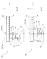
도 2는 도 1에 나타내는 실장 장치에 있어서 리니어 스케일이 열팽창한 경우의 기본 동작을 나타내는 설명도이며, (a)는 제1 위치에서의 상태, (b)는 카메라측 엔코더 헤드에서 검출한 리니어 스케일의 눈금 위치에 본딩 헤드측 엔코더 헤드의 중심선이 일치하도록 베이스를 이동한 상태를 도시한다.
도 3은 도 1에 나타내는 실장 장치에 있어서 베이스가 열팽창한 경우의 기본동작을 나타내는 설명도이며, (a)는 제1 위치에서의 상태, (b)는 카메라측 엔코더 헤드에서 검출한 리니어 스케일의 눈금 위치에 본딩 헤드측 엔코더 헤드의 중심선이 일치하도록 베이스를 이동한 상태를 도시한다.
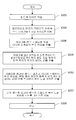
도 4는 도 1에 나타내는 실장 장치의 동작을 도시하는 흐름도이다.
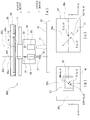
도 5는 도 4에 나타내는 실장 장치의 동작에 있어서, 베이스가 제1 위치에 있는 상태의 입면도(a)와, 본딩 툴의 중심 위치와 본딩 툴에 흡착된 반도체 다이의 상대 위치를 도시하는 설명도(b)와, 제1 위치에 있어서의 카메라의 시야(c)를 도시하는 설명도이다.
도 6은 도 4에 나타내는 실장 장치의 동작에 있어서, 카메라측 엔코더 헤드에서 검출한 리니어 스케일의 눈금 위치에 본딩 헤드측 엔코더 헤드의 중심선이 일치하도록 베이스를 이동한 상태를 도시하는 입면도(a)와, 그 때의 본딩 툴과 기판의 얼라인먼트 마크의 위치 관계를 도시하는 설명도(b)이다.
도 7은 도 1에 나타내는 실장 장치의 다른 동작을 도시하는 흐름도이다.
도 8은 도 1에 나타내는 실장 장치의 다른 동작을 도시하는 흐름도이다.
도 9는 도 8에 나타내는 실장 장치의 동작에 있어서, 목표 눈금 위치에 본딩 헤드측 엔코더 헤드의 중심선이 일치하도록 베이스를 이동한 상태를 도시하는 입면도(a)와, 그 때의 본딩 툴과 기판의 얼라인먼트 마크의 위치 관계를 도시하는 설명도(b)이다.
도 10은 도 1에 나타내는 실장 장치의 다른 동작을 도시하는 흐름도이다.
11 가이드 레일
12 리니어 모터
13 본딩 스테이지
15 반도체 다이
16 기판
17 얼라인먼트 마크
20 본딩 헤드
21 본딩 툴
22x, 22y, 22z, 31a, 32a 중심선
25 카메라
26x X 방향 중심선
26y Y 방향 중심선
26z 광축
27 시야
31 본딩 헤드측 엔코더 헤드
32 카메라측 엔코더 헤드
33, 33' 리니어 스케일
34, 34' 눈금
40 하측 카메라
41 시야
50 제어부
100 실장 장치
BH, D, S 중심 위치
C 위치
N 눈금 위치
N2 목표 눈금 위치
ΔBH, ΔC 위치차
ΔH 간격
Claims (9)
- 제1 물체를 제2 물체에 대하여 위치 결정하는 장치로서,
상기 제2 물체에 대하여 직선 이동하는 이동체와,
상기 이동체에 부착되어 상기 제1 물체를 유지하는 유지부와,
상기 이동체의 이동 방향을 따라 상기 유지부와 소정의 간격을 두고 상기 이동체에 부착되고, 상기 제2 물체의 위치를 특정하는 위치 특정 수단과,
상기 이동체의 상기 이동 방향을 따라 배치되어, 상기 이동 방향을 따라 복수의 눈금을 갖는 스케일과,
상기 유지부에 대응하여 상기 이동체에 부착되어, 상기 눈금에 기초하여 상기 유지부의 위치를 검출하는 제1 위치 검출부와,
상기 위치 특정 수단에 대응하여 상기 제1 위치 검출부와 상기 소정의 간격을 두고 상기 이동체에 부착되어, 특정된 상기 제2 물체의 위치에 대응하는 상기 스케일의 눈금 위치를 검출하는 제2 위치 검출부와,
상기 제1 위치 검출부가 상기 눈금 위치를 검출하는 위치에 상기 이동체를 이동시켜 상기 제1 물체를 상기 제2 물체에 대하여 위치 결정을 하는 제어부를 구비하는 장치. - 제1항에 있어서,
상기 제1 물체는 반도체 다이이고,
상기 제2 물체는 상기 반도체 다이가 설치되는, 기판 또는 다른 반도체 다이이며,
상기 장치는 상기 제1 물체를 상기 제2 물체의 미리 정해진 영역에 위치 결정을 하는 장치인 것을 특징으로 하는 장치. - 제1항에 있어서,
상기 위치 특정 수단은 광학적으로 상기 제2 물체의 위치를 특정하는 카메라이며,
상기 제어부는
상기 위치 특정 수단을 상기 제2 물체의 특정 영역이 상기 위치 특정 수단의 시야에 들어가는 제1 위치로 상기 이동체를 이동시키고, 제2 위치 검출부에서 상기 제1 위치에서의 상기 스케일의 상기 눈금 위치를 검출하고,
상기 위치 특정 수단에서 상기 제2 물체의 상기 특정 영역을 촬상한 화상에 기초하여 상기 특정 영역에 대한 상기 위치 특정 수단의 제1 상대 위치를 검출하고,
상기 제1 상대 위치에 기초하여, 상기 제1 물체를 상기 제2 물체에 대하여 위치 결정을 할 때의 상기 이동체의 위치를 보정하는 보정량을 산출하는 것을 특징으로 하는 장치. - 제2항에 있어서,
상기 위치 특정 수단은 광학적으로 상기 제2 물체의 위치를 특정하는 카메라이며,
상기 제어부는
상기 위치 특정 수단을 상기 제2 물체의 특정 영역이 상기 위치 특정 수단의 시야에 들어가는 제1 위치로 상기 이동체를 이동시키고, 제2 위치 검출부에서 상기 제1 위치에서의 상기 스케일의 상기 눈금 위치를 검출하고,
상기 위치 특정 수단에서 상기 제2 물체의 상기 특정 영역을 촬상한 화상에 기초하여 상기 특정 영역에 대한 상기 위치 특정 수단의 제1 상대 위치를 검출하고,
상기 제1 상대 위치에 기초하여 상기 제1 물체를 상기 제2 물체에 대하여 위치 결정을 할 때의 상기 이동체의 위치를 보정하는 보정량을 산출하는 것을 특징으로 하는 장치. - 제1항 내지 제4항 중 어느 한 항에 있어서,
상기 유지부의 유지면측에 배치되어, 유지면에 대한 상기 제1 물체의 제2 상대 위치를 특정하는 유지 위치 특정 수단을 더 포함하고,
상기 제어부는
상기 제2 상대 위치에 기초하여 상기 제1 물체를 상기 제2 물체에 대하여 위치 결정을 할 때의 상기 이동체의 위치를 보정하는 보정량을 산출하는 것을 특징으로 하는 장치. - 제3항에 있어서,
상기 제어부는 상기 보정량에 기초하여 상기 스케일에서의 목표 눈금 위치를 산출하는 것을 특징으로 하는 장치. - 제4항에 있어서,
상기 제어부는 상기 보정량에 기초하여 상기 스케일에서의 목표 눈금 위치를 산출하는 것을 특징으로 하는 장치. - 제5항에 있어서,
상기 제어부는 상기 보정량에 기초하여 상기 스케일에서의 목표 눈금 위치를 산출하는 것을 특징으로 하는 장치. - 제1 물체를 제2 물체에 대하여 위치 결정하는 방법으로서,
유지부에 의해 상기 제1 물체를 유지하는 공정과,
상기 제1 물체를 유지하는 상기 유지부 및 위치 특정 수단이 설치된 이동체를 소정의 위치로 이동시키는 이동 공정과,
상기 이동체의 이동 방향을 따라 상기 유지부와 소정의 간격을 두고 상기 이동체에 부착된 상기 위치 특정 수단에 의해, 상기 제2 물체의 위치를 특정하는 위치 특정 공정과,
상기 위치 특정 수단에 대응하여 제1 위치 검출부와 상기 소정의 간격을 두고 상기 이동체에 부착된 제2 위치 검출부에 의해, 특정된 상기 제2 물체의 위치에 대응하는 스케일의 눈금 위치를 검출하는 위치 검출 공정과,
상기 이동체에 배치된 제1 위치 검출부에 의해 상기 스케일의 눈금을 읽어내고, 상기 눈금 위치를 검출하는 위치에 상기 유지부를 이동시켜 상기 제1 물체를 상기 제2 물체에 대하여 위치 결정을 하는 위치 결정 공정을 포함하는 방법.
Applications Claiming Priority (3)
| Application Number | Priority Date | Filing Date | Title |
|---|---|---|---|
| JPJP-P-2017-136065 | 2017-07-12 | ||
| JP2017136065 | 2017-07-12 | ||
| PCT/JP2018/026292 WO2019013274A1 (ja) | 2017-07-12 | 2018-07-12 | 第1物体を第2物体に対して位置決めする装置及び方法 |
Publications (2)
| Publication Number | Publication Date |
|---|---|
| KR20200021539A true KR20200021539A (ko) | 2020-02-28 |
| KR102362976B1 KR102362976B1 (ko) | 2022-02-15 |
Family
ID=65002091
Family Applications (1)
| Application Number | Title | Priority Date | Filing Date |
|---|---|---|---|
| KR1020207003992A Active KR102362976B1 (ko) | 2017-07-12 | 2018-07-12 | 제1 물체를 제2 물체에 대하여 위치 결정하는 장치 및 방법 |
Country Status (7)
| Country | Link |
|---|---|
| US (1) | US11139193B2 (ko) |
| JP (1) | JP6787612B2 (ko) |
| KR (1) | KR102362976B1 (ko) |
| CN (1) | CN111066130B (ko) |
| SG (1) | SG11202001940PA (ko) |
| TW (1) | TWI684235B (ko) |
| WO (1) | WO2019013274A1 (ko) |
Cited By (1)
| Publication number | Priority date | Publication date | Assignee | Title |
|---|---|---|---|---|
| KR20240038572A (ko) * | 2022-09-16 | 2024-03-25 | 가부시키가이샤 스크린 홀딩스 | 묘화 장치 및 묘화 방법 |
Families Citing this family (8)
| Publication number | Priority date | Publication date | Assignee | Title |
|---|---|---|---|---|
| US11217471B2 (en) * | 2019-03-06 | 2022-01-04 | Rohinni, LLC | Multi-axis movement for transfer of semiconductor devices |
| JP7291586B2 (ja) * | 2019-09-19 | 2023-06-15 | ファスフォードテクノロジ株式会社 | ダイボンディング装置および半導体装置の製造方法 |
| CN112945092B (zh) * | 2021-01-27 | 2023-03-28 | 深圳市卓兴半导体科技有限公司 | 一种多工位设备的模板定位方法及系统 |
| JP2023042403A (ja) * | 2021-09-14 | 2023-03-27 | ファスフォードテクノロジ株式会社 | 実装装置および半導体装置の製造方法 |
| JP7396741B2 (ja) * | 2021-11-16 | 2023-12-12 | 株式会社新川 | 実装装置、実装方法および実装制御プログラム |
| JP7582928B2 (ja) * | 2021-11-25 | 2024-11-13 | キヤノン株式会社 | 接合装置および接合方法 |
| JP2024176665A (ja) * | 2023-06-09 | 2024-12-19 | 株式会社新川 | 実装装置および実装装置が備えるボンディングヘッドの変位検出方法 |
| EP4657511A1 (en) * | 2024-05-27 | 2025-12-03 | Etel S.A. | Die bonding apparatus and die positioning method using the die bonding apparatus |
Citations (3)
| Publication number | Priority date | Publication date | Assignee | Title |
|---|---|---|---|---|
| JP2001203234A (ja) | 2000-01-21 | 2001-07-27 | Shinkawa Ltd | ボンディング装置およびボンディング方法 |
| KR101472434B1 (ko) * | 2012-09-07 | 2014-12-12 | 야마하하쓰도키 가부시키가이샤 | 전자 부품 실장 장치 및 실장 위치 보정 데이터 작성 방법 |
| KR20160118925A (ko) * | 2015-04-02 | 2016-10-12 | 파스포드 테크놀로지 주식회사 | 본딩 장치 및 본딩 방법 |
Family Cites Families (8)
| Publication number | Priority date | Publication date | Assignee | Title |
|---|---|---|---|---|
| JP3333060B2 (ja) * | 1995-04-11 | 2002-10-07 | 東レエンジニアリング株式会社 | チップボンディング方法及びその装置 |
| JP2930093B2 (ja) * | 1995-08-18 | 1999-08-03 | 澁谷工業株式会社 | ボンディング方法 |
| JP3143826B2 (ja) * | 1996-12-29 | 2001-03-07 | 澁谷工業株式会社 | ディスペンサ付きボンディング装置 |
| JP2004146776A (ja) * | 2002-08-29 | 2004-05-20 | Shinko Electric Ind Co Ltd | フリップチップ実装装置及びフリップチップ実装方法 |
| JP5365618B2 (ja) * | 2010-12-24 | 2013-12-11 | ソニー株式会社 | 位置調整装置及び位置調整方法 |
| TWI545663B (zh) * | 2014-05-07 | 2016-08-11 | 新川股份有限公司 | 接合裝置以及接合方法 |
| JP5828943B1 (ja) * | 2014-08-11 | 2015-12-09 | 株式会社新川 | 電子部品の実装装置 |
| JP6307730B1 (ja) | 2016-09-29 | 2018-04-11 | 株式会社新川 | 半導体装置の製造方法、及び実装装置 |
-
2018
- 2018-07-10 TW TW107123830A patent/TWI684235B/zh active
- 2018-07-12 WO PCT/JP2018/026292 patent/WO2019013274A1/ja not_active Ceased
- 2018-07-12 US US16/632,870 patent/US11139193B2/en active Active
- 2018-07-12 SG SG11202001940PA patent/SG11202001940PA/en unknown
- 2018-07-12 KR KR1020207003992A patent/KR102362976B1/ko active Active
- 2018-07-12 CN CN201880058440.9A patent/CN111066130B/zh active Active
- 2018-07-12 JP JP2019529776A patent/JP6787612B2/ja active Active
Patent Citations (3)
| Publication number | Priority date | Publication date | Assignee | Title |
|---|---|---|---|---|
| JP2001203234A (ja) | 2000-01-21 | 2001-07-27 | Shinkawa Ltd | ボンディング装置およびボンディング方法 |
| KR101472434B1 (ko) * | 2012-09-07 | 2014-12-12 | 야마하하쓰도키 가부시키가이샤 | 전자 부품 실장 장치 및 실장 위치 보정 데이터 작성 방법 |
| KR20160118925A (ko) * | 2015-04-02 | 2016-10-12 | 파스포드 테크놀로지 주식회사 | 본딩 장치 및 본딩 방법 |
Cited By (1)
| Publication number | Priority date | Publication date | Assignee | Title |
|---|---|---|---|---|
| KR20240038572A (ko) * | 2022-09-16 | 2024-03-25 | 가부시키가이샤 스크린 홀딩스 | 묘화 장치 및 묘화 방법 |
Also Published As
| Publication number | Publication date |
|---|---|
| KR102362976B1 (ko) | 2022-02-15 |
| JPWO2019013274A1 (ja) | 2020-04-16 |
| JP6787612B2 (ja) | 2020-11-18 |
| WO2019013274A1 (ja) | 2019-01-17 |
| TW201909327A (zh) | 2019-03-01 |
| SG11202001940PA (en) | 2020-04-29 |
| CN111066130A (zh) | 2020-04-24 |
| TWI684235B (zh) | 2020-02-01 |
| US11139193B2 (en) | 2021-10-05 |
| CN111066130B (zh) | 2023-05-02 |
| US20200251369A1 (en) | 2020-08-06 |
Similar Documents
| Publication | Publication Date | Title |
|---|---|---|
| KR102362976B1 (ko) | 제1 물체를 제2 물체에 대하여 위치 결정하는 장치 및 방법 | |
| KR102680413B1 (ko) | 반도체 장치의 제조 장치, 및 반도체 장치의 제조 방법 | |
| US10743447B2 (en) | Component mounting machine | |
| JP5174583B2 (ja) | 電子部品実装装置の制御方法 | |
| KR20130012928A (ko) | 전자 부품 반송 장치 및 전자 부품 반송 방법 | |
| KR20130035263A (ko) | 다이 본더 및 반도체 제조 방법 | |
| KR20160091811A (ko) | 본딩 장치 및 본딩 방법 | |
| JP6370299B2 (ja) | 部品実装装置、その制御方法および部品実装装置用プログラム | |
| JP2001308148A (ja) | 位置合わせ装置及び位置合わせ方法 | |
| JPWO2017064776A1 (ja) | 部品実装装置 | |
| JP7072264B2 (ja) | 対象物に対して移動体を直線移動させる装置および方法 | |
| JPH077028A (ja) | 半導体位置合せ方法 | |
| JP4648964B2 (ja) | マーク認識システム、マーク認識方法および表面実装機 | |
| JP3265143B2 (ja) | 部品搭載方法および装置 | |
| EP0989601B1 (en) | Method of and apparatus for bonding component | |
| JP2707548B2 (ja) | 視覚認識装置の座標補正方法 | |
| CN112514553A (zh) | 表面安装机 | |
| KR20150113130A (ko) | 실장 방법 및 실장 장치 | |
| JP6475264B2 (ja) | 部品実装機 | |
| JP2011181675A (ja) | 回路部品の実装装置 | |
| CN107926148A (zh) | 模型数据生成装置、模型数据的生成方法、搭载基准点决定装置及搭载基准点的决定方法 | |
| CN117337620A (zh) | 元件移载装置 | |
| JP2002141362A (ja) | 電子部品の実装装置 | |
| KR20110034152A (ko) | 카메라를 이용한 작업위치 자동 결정 방법 | |
| JPH0645786A (ja) | 高さ調整手段を備えた部品実装装置 |
Legal Events
| Date | Code | Title | Description |
|---|---|---|---|
| A201 | Request for examination | ||
| PA0105 | International application |
St.27 status event code: A-0-1-A10-A15-nap-PA0105 |
|
| PA0201 | Request for examination |
St.27 status event code: A-1-2-D10-D11-exm-PA0201 |
|
| PG1501 | Laying open of application |
St.27 status event code: A-1-1-Q10-Q12-nap-PG1501 |
|
| D13-X000 | Search requested |
St.27 status event code: A-1-2-D10-D13-srh-X000 |
|
| D14-X000 | Search report completed |
St.27 status event code: A-1-2-D10-D14-srh-X000 |
|
| E902 | Notification of reason for refusal | ||
| PE0902 | Notice of grounds for rejection |
St.27 status event code: A-1-2-D10-D21-exm-PE0902 |
|
| T11-X000 | Administrative time limit extension requested |
St.27 status event code: U-3-3-T10-T11-oth-X000 |
|
| P11-X000 | Amendment of application requested |
St.27 status event code: A-2-2-P10-P11-nap-X000 |
|
| P13-X000 | Application amended |
St.27 status event code: A-2-2-P10-P13-nap-X000 |
|
| E701 | Decision to grant or registration of patent right | ||
| PE0701 | Decision of registration |
St.27 status event code: A-1-2-D10-D22-exm-PE0701 |
|
| GRNT | Written decision to grant | ||
| PR0701 | Registration of establishment |
St.27 status event code: A-2-4-F10-F11-exm-PR0701 |
|
| PR1002 | Payment of registration fee |
St.27 status event code: A-2-2-U10-U12-oth-PR1002 Fee payment year number: 1 |
|
| PG1601 | Publication of registration |
St.27 status event code: A-4-4-Q10-Q13-nap-PG1601 |
|
| PN2301 | Change of applicant |
St.27 status event code: A-5-5-R10-R11-asn-PN2301 |
|
| R11 | Change to the name of applicant or owner or transfer of ownership requested |
Free format text: ST27 STATUS EVENT CODE: A-5-5-R10-R11-ASN-PN2301 (AS PROVIDED BY THE NATIONAL OFFICE) |
|
| PN2301 | Change of applicant |
St.27 status event code: A-5-5-R10-R14-asn-PN2301 |
|
| R14 | Transfer of ownership recorded |
Free format text: ST27 STATUS EVENT CODE: A-5-5-R10-R14-ASN-PN2301 (AS PROVIDED BY THE NATIONAL OFFICE) |
|
| P22-X000 | Classification modified |
St.27 status event code: A-4-4-P10-P22-nap-X000 |