KR20200021797A - 반도체 소자 - Google Patents
반도체 소자 Download PDFInfo
- Publication number
- KR20200021797A KR20200021797A KR1020180097598A KR20180097598A KR20200021797A KR 20200021797 A KR20200021797 A KR 20200021797A KR 1020180097598 A KR1020180097598 A KR 1020180097598A KR 20180097598 A KR20180097598 A KR 20180097598A KR 20200021797 A KR20200021797 A KR 20200021797A
- Authority
- KR
- South Korea
- Prior art keywords
- disposed
- semiconductor layer
- recess
- electrode
- pad
- Prior art date
- Legal status (The legal status is an assumption and is not a legal conclusion. Google has not performed a legal analysis and makes no representation as to the accuracy of the status listed.)
- Granted
Links
- 239000004065 semiconductor Substances 0.000 claims abstract description 266
- 239000000758 substrate Substances 0.000 claims abstract description 36
- 230000000149 penetrating effect Effects 0.000 claims abstract description 6
- 238000000034 method Methods 0.000 claims description 24
- 239000010410 layer Substances 0.000 description 353
- 239000000463 material Substances 0.000 description 23
- XLOMVQKBTHCTTD-UHFFFAOYSA-N Zinc monoxide Chemical compound [Zn]=O XLOMVQKBTHCTTD-UHFFFAOYSA-N 0.000 description 14
- 238000005530 etching Methods 0.000 description 14
- 229910052751 metal Inorganic materials 0.000 description 13
- 239000002184 metal Substances 0.000 description 13
- 229910052782 aluminium Inorganic materials 0.000 description 12
- 230000008569 process Effects 0.000 description 12
- 239000002019 doping agent Substances 0.000 description 11
- 230000000903 blocking effect Effects 0.000 description 10
- 239000000203 mixture Substances 0.000 description 9
- 239000010408 film Substances 0.000 description 8
- 230000003647 oxidation Effects 0.000 description 8
- 238000007254 oxidation reaction Methods 0.000 description 8
- XAGFODPZIPBFFR-UHFFFAOYSA-N aluminium Chemical compound [Al] XAGFODPZIPBFFR-UHFFFAOYSA-N 0.000 description 7
- 150000001875 compounds Chemical class 0.000 description 7
- 239000011787 zinc oxide Substances 0.000 description 7
- 239000000356 contaminant Substances 0.000 description 6
- 229910052738 indium Inorganic materials 0.000 description 6
- 229910052725 zinc Inorganic materials 0.000 description 6
- 239000011701 zinc Substances 0.000 description 6
- 238000005229 chemical vapour deposition Methods 0.000 description 5
- 229910052737 gold Inorganic materials 0.000 description 5
- 229910002704 AlGaN Inorganic materials 0.000 description 4
- 230000008901 benefit Effects 0.000 description 4
- 238000004891 communication Methods 0.000 description 4
- 239000006185 dispersion Substances 0.000 description 4
- 230000000694 effects Effects 0.000 description 4
- 230000017525 heat dissipation Effects 0.000 description 4
- 238000005286 illumination Methods 0.000 description 4
- 238000004519 manufacturing process Methods 0.000 description 4
- 238000004549 pulsed laser deposition Methods 0.000 description 4
- 238000000926 separation method Methods 0.000 description 4
- 229910052709 silver Inorganic materials 0.000 description 4
- 229910052718 tin Inorganic materials 0.000 description 4
- 229910052804 chromium Inorganic materials 0.000 description 3
- 230000007547 defect Effects 0.000 description 3
- 238000000605 extraction Methods 0.000 description 3
- 229910052733 gallium Inorganic materials 0.000 description 3
- 229910052735 hafnium Inorganic materials 0.000 description 3
- 229910052741 iridium Inorganic materials 0.000 description 3
- VRIVJOXICYMTAG-IYEMJOQQSA-L iron(ii) gluconate Chemical compound [Fe+2].OC[C@@H](O)[C@@H](O)[C@H](O)[C@@H](O)C([O-])=O.OC[C@@H](O)[C@@H](O)[C@H](O)[C@@H](O)C([O-])=O VRIVJOXICYMTAG-IYEMJOQQSA-L 0.000 description 3
- 230000004048 modification Effects 0.000 description 3
- 238000012986 modification Methods 0.000 description 3
- 229910052759 nickel Inorganic materials 0.000 description 3
- 230000003287 optical effect Effects 0.000 description 3
- 229910052763 palladium Inorganic materials 0.000 description 3
- 230000035515 penetration Effects 0.000 description 3
- 229910052697 platinum Inorganic materials 0.000 description 3
- 229910052703 rhodium Inorganic materials 0.000 description 3
- 229910052710 silicon Inorganic materials 0.000 description 3
- HBMJWWWQQXIZIP-UHFFFAOYSA-N silicon carbide Chemical compound [Si+]#[C-] HBMJWWWQQXIZIP-UHFFFAOYSA-N 0.000 description 3
- 238000004544 sputter deposition Methods 0.000 description 3
- 229910052719 titanium Inorganic materials 0.000 description 3
- 229910018072 Al 2 O 3 Inorganic materials 0.000 description 2
- -1 GaN Chemical class 0.000 description 2
- GYHNNYVSQQEPJS-UHFFFAOYSA-N Gallium Chemical compound [Ga] GYHNNYVSQQEPJS-UHFFFAOYSA-N 0.000 description 2
- 229910001218 Gallium arsenide Inorganic materials 0.000 description 2
- OAICVXFJPJFONN-UHFFFAOYSA-N Phosphorus Chemical compound [P] OAICVXFJPJFONN-UHFFFAOYSA-N 0.000 description 2
- 229910019897 RuOx Inorganic materials 0.000 description 2
- 229910004298 SiO 2 Inorganic materials 0.000 description 2
- 229910010413 TiO 2 Inorganic materials 0.000 description 2
- 239000003086 colorant Substances 0.000 description 2
- 239000004020 conductor Substances 0.000 description 2
- 230000007423 decrease Effects 0.000 description 2
- 238000011161 development Methods 0.000 description 2
- 238000010586 diagram Methods 0.000 description 2
- JAONJTDQXUSBGG-UHFFFAOYSA-N dialuminum;dizinc;oxygen(2-) Chemical compound [O-2].[O-2].[O-2].[O-2].[O-2].[Al+3].[Al+3].[Zn+2].[Zn+2] JAONJTDQXUSBGG-UHFFFAOYSA-N 0.000 description 2
- 238000001312 dry etching Methods 0.000 description 2
- 230000007613 environmental effect Effects 0.000 description 2
- 238000010438 heat treatment Methods 0.000 description 2
- 238000002248 hydride vapour-phase epitaxy Methods 0.000 description 2
- APFVFJFRJDLVQX-UHFFFAOYSA-N indium atom Chemical compound [In] APFVFJFRJDLVQX-UHFFFAOYSA-N 0.000 description 2
- 238000002347 injection Methods 0.000 description 2
- 239000007924 injection Substances 0.000 description 2
- 239000011810 insulating material Substances 0.000 description 2
- 239000007769 metal material Substances 0.000 description 2
- TWNQGVIAIRXVLR-UHFFFAOYSA-N oxo(oxoalumanyloxy)alumane Chemical compound O=[Al]O[Al]=O TWNQGVIAIRXVLR-UHFFFAOYSA-N 0.000 description 2
- 229920002120 photoresistant polymer Polymers 0.000 description 2
- 238000000623 plasma-assisted chemical vapour deposition Methods 0.000 description 2
- 238000012545 processing Methods 0.000 description 2
- 230000004044 response Effects 0.000 description 2
- 229910052711 selenium Inorganic materials 0.000 description 2
- 239000011669 selenium Substances 0.000 description 2
- 229910010271 silicon carbide Inorganic materials 0.000 description 2
- 239000002356 single layer Substances 0.000 description 2
- 230000001954 sterilising effect Effects 0.000 description 2
- SKRWFPLZQAAQSU-UHFFFAOYSA-N stibanylidynetin;hydrate Chemical compound O.[Sn].[Sb] SKRWFPLZQAAQSU-UHFFFAOYSA-N 0.000 description 2
- 238000001039 wet etching Methods 0.000 description 2
- WUPHOULIZUERAE-UHFFFAOYSA-N 3-(oxolan-2-yl)propanoic acid Chemical compound OC(=O)CCC1CCCO1 WUPHOULIZUERAE-UHFFFAOYSA-N 0.000 description 1
- 229910017083 AlN Inorganic materials 0.000 description 1
- 229910000980 Aluminium gallium arsenide Inorganic materials 0.000 description 1
- 229910018229 Al—Ga Inorganic materials 0.000 description 1
- 229910002601 GaN Inorganic materials 0.000 description 1
- 229910005540 GaP Inorganic materials 0.000 description 1
- BUGBHKTXTAQXES-UHFFFAOYSA-N Selenium Chemical compound [Se] BUGBHKTXTAQXES-UHFFFAOYSA-N 0.000 description 1
- 229910020286 SiOxNy Inorganic materials 0.000 description 1
- 229910020776 SixNy Inorganic materials 0.000 description 1
- 229910020781 SixOy Inorganic materials 0.000 description 1
- DZLPZFLXRVRDAE-UHFFFAOYSA-N [O--].[O--].[O--].[O--].[Al+3].[Zn++].[In+3] Chemical compound [O--].[O--].[O--].[O--].[Al+3].[Zn++].[In+3] DZLPZFLXRVRDAE-UHFFFAOYSA-N 0.000 description 1
- 229910052789 astatine Inorganic materials 0.000 description 1
- 230000004888 barrier function Effects 0.000 description 1
- 229910052980 cadmium sulfide Inorganic materials 0.000 description 1
- UHYPYGJEEGLRJD-UHFFFAOYSA-N cadmium(2+);selenium(2-) Chemical compound [Se-2].[Cd+2] UHYPYGJEEGLRJD-UHFFFAOYSA-N 0.000 description 1
- 238000006243 chemical reaction Methods 0.000 description 1
- 230000007797 corrosion Effects 0.000 description 1
- 238000005260 corrosion Methods 0.000 description 1
- 230000008878 coupling Effects 0.000 description 1
- 238000010168 coupling process Methods 0.000 description 1
- 238000005859 coupling reaction Methods 0.000 description 1
- 230000002950 deficient Effects 0.000 description 1
- 238000009792 diffusion process Methods 0.000 description 1
- 238000005401 electroluminescence Methods 0.000 description 1
- 238000005538 encapsulation Methods 0.000 description 1
- 238000005516 engineering process Methods 0.000 description 1
- 238000000407 epitaxy Methods 0.000 description 1
- 229910052731 fluorine Inorganic materials 0.000 description 1
- YZZNJYQZJKSEER-UHFFFAOYSA-N gallium tin Chemical compound [Ga].[Sn] YZZNJYQZJKSEER-UHFFFAOYSA-N 0.000 description 1
- 229910052732 germanium Inorganic materials 0.000 description 1
- 230000006872 improvement Effects 0.000 description 1
- AMGQUBHHOARCQH-UHFFFAOYSA-N indium;oxotin Chemical compound [In].[Sn]=O AMGQUBHHOARCQH-UHFFFAOYSA-N 0.000 description 1
- HRHKULZDDYWVBE-UHFFFAOYSA-N indium;oxozinc;tin Chemical compound [In].[Sn].[Zn]=O HRHKULZDDYWVBE-UHFFFAOYSA-N 0.000 description 1
- 238000009413 insulation Methods 0.000 description 1
- 239000004973 liquid crystal related substance Substances 0.000 description 1
- 230000005012 migration Effects 0.000 description 1
- 238000013508 migration Methods 0.000 description 1
- 238000000465 moulding Methods 0.000 description 1
- GNRSAWUEBMWBQH-UHFFFAOYSA-N nickel(II) oxide Inorganic materials [Ni]=O GNRSAWUEBMWBQH-UHFFFAOYSA-N 0.000 description 1
- 150000004767 nitrides Chemical class 0.000 description 1
- 229910052757 nitrogen Inorganic materials 0.000 description 1
- 230000005693 optoelectronics Effects 0.000 description 1
- 230000010355 oscillation Effects 0.000 description 1
- 230000001590 oxidative effect Effects 0.000 description 1
- 229910052760 oxygen Inorganic materials 0.000 description 1
- 239000012071 phase Substances 0.000 description 1
- 229910052698 phosphorus Inorganic materials 0.000 description 1
- 238000002360 preparation method Methods 0.000 description 1
- 239000002096 quantum dot Substances 0.000 description 1
- 230000006798 recombination Effects 0.000 description 1
- 238000005215 recombination Methods 0.000 description 1
- 238000009877 rendering Methods 0.000 description 1
- 239000010703 silicon Substances 0.000 description 1
- 239000000243 solution Substances 0.000 description 1
- 230000003595 spectral effect Effects 0.000 description 1
- 230000007480 spreading Effects 0.000 description 1
- 238000003892 spreading Methods 0.000 description 1
- 238000004659 sterilization and disinfection Methods 0.000 description 1
- 239000010409 thin film Substances 0.000 description 1
- 229910001887 tin oxide Inorganic materials 0.000 description 1
- 230000007704 transition Effects 0.000 description 1
- 238000004627 transmission electron microscopy Methods 0.000 description 1
- 239000012780 transparent material Substances 0.000 description 1
- YVTHLONGBIQYBO-UHFFFAOYSA-N zinc indium(3+) oxygen(2-) Chemical compound [O--].[Zn++].[In+3] YVTHLONGBIQYBO-UHFFFAOYSA-N 0.000 description 1
Images







Classifications
-
- H—ELECTRICITY
- H10—SEMICONDUCTOR DEVICES; ELECTRIC SOLID-STATE DEVICES NOT OTHERWISE PROVIDED FOR
- H10H—INORGANIC LIGHT-EMITTING SEMICONDUCTOR DEVICES HAVING POTENTIAL BARRIERS
- H10H20/00—Individual inorganic light-emitting semiconductor devices having potential barriers, e.g. light-emitting diodes [LED]
- H10H20/80—Constructional details
- H10H20/81—Bodies
- H10H20/819—Bodies characterised by their shape, e.g. curved or truncated substrates
- H10H20/82—Roughened surfaces, e.g. at the interface between epitaxial layers
-
- H01L33/22—
-
- H01L33/14—
-
- H01L33/24—
-
- H01L33/38—
-
- H01L33/62—
-
- H—ELECTRICITY
- H10—SEMICONDUCTOR DEVICES; ELECTRIC SOLID-STATE DEVICES NOT OTHERWISE PROVIDED FOR
- H10H—INORGANIC LIGHT-EMITTING SEMICONDUCTOR DEVICES HAVING POTENTIAL BARRIERS
- H10H20/00—Individual inorganic light-emitting semiconductor devices having potential barriers, e.g. light-emitting diodes [LED]
- H10H20/80—Constructional details
- H10H20/81—Bodies
- H10H20/816—Bodies having carrier transport control structures, e.g. highly-doped semiconductor layers or current-blocking structures
-
- H—ELECTRICITY
- H10—SEMICONDUCTOR DEVICES; ELECTRIC SOLID-STATE DEVICES NOT OTHERWISE PROVIDED FOR
- H10H—INORGANIC LIGHT-EMITTING SEMICONDUCTOR DEVICES HAVING POTENTIAL BARRIERS
- H10H20/00—Individual inorganic light-emitting semiconductor devices having potential barriers, e.g. light-emitting diodes [LED]
- H10H20/80—Constructional details
- H10H20/81—Bodies
- H10H20/819—Bodies characterised by their shape, e.g. curved or truncated substrates
- H10H20/821—Bodies characterised by their shape, e.g. curved or truncated substrates of the light-emitting regions, e.g. non-planar junctions
-
- H—ELECTRICITY
- H10—SEMICONDUCTOR DEVICES; ELECTRIC SOLID-STATE DEVICES NOT OTHERWISE PROVIDED FOR
- H10H—INORGANIC LIGHT-EMITTING SEMICONDUCTOR DEVICES HAVING POTENTIAL BARRIERS
- H10H20/00—Individual inorganic light-emitting semiconductor devices having potential barriers, e.g. light-emitting diodes [LED]
- H10H20/80—Constructional details
- H10H20/83—Electrodes
- H10H20/831—Electrodes characterised by their shape
-
- H—ELECTRICITY
- H10—SEMICONDUCTOR DEVICES; ELECTRIC SOLID-STATE DEVICES NOT OTHERWISE PROVIDED FOR
- H10H—INORGANIC LIGHT-EMITTING SEMICONDUCTOR DEVICES HAVING POTENTIAL BARRIERS
- H10H20/00—Individual inorganic light-emitting semiconductor devices having potential barriers, e.g. light-emitting diodes [LED]
- H10H20/80—Constructional details
- H10H20/85—Packages
- H10H20/857—Interconnections, e.g. lead-frames, bond wires or solder balls
Landscapes
- Led Devices (AREA)
Abstract
상기 제2 패드는 상기 제2 전극 상에서 상기 리세스의 상부로 연장하며 배치되는 반도체 소자를 개시한다.
Description
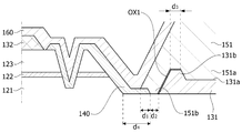
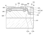
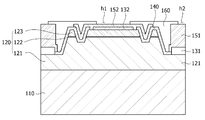
도 2는 도 1에서 AA'로 절단된 단면도이고,
도 3a는 도 2에서 K부분의 확대도이고,
도 3b는 도 3a에서 L부분의 확대도이고,
도 4는 도 1에서 BB'로 절단된 단면도이고,
도 5는 다른 실시예에 따른 반도체 소자의 평면도이고,
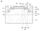
도 6은 도 5에서 CC'로 절단된 단면도이고,
도 7은 도 1의 변형예이고,
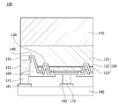
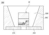
도 8은 실시예에 따른 반도체 소자 패키지의 개념도이고,
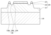
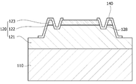
도 9a 내지 도 9h는 일 실시예에 따른 반도체 소자의 제조 방법을 도시한 도면이다.
Claims (11)
- 기판;
상기 기판 상에 배치되는 제1 도전형 반도체층, 제2 도전형 반도체층, 및 상기 제1 도전형 반도체층과 상기 제2 도전형 반도체층 사이에 배치되는 활성층을 포함하고, 상기 제2 도전형 반도체층 및 상기 활성층을 관통하는 리세스를 포함하는 발광 구조물;
상기 발광 구조물 상에 배치되고, 상기 제1 도전형 반도체층과 전기적으로 연결되는 제1 전극;
상기 발광 구조물 상에 배치되고, 상기 제2 도전형 반도체층과 전기적으로 연결되는 제2 전극;
상기 제1 전극 상에 배치되는 제1 패드; 및
상기 제2 전극 상에 배치되는 제2 패드;를 포함하고,
상기 리세스는 상기 제2 도전형 반도체층 및 상기 활성층을 활성 영역 및 비활성 영역으로 분리하고,
상기 리세스는 상기 활성 영역을 둘러싸도록 연장되어 배치되고,
상기 제2 패드는 상기 제2 전극 상에서 상기 리세스의 상부로 연장하며 배치되는 반도체 소자.
- 제1항에 있어서,
상기 리세스는,
바닥면;
상기 바닥면과 연결되며 상기 활성 영역에 인접하는 내측 경사면; 및
상기 바닥면과 연결되며 상기 내측 경사면과 대향하는 외측 경사면;을 포함하고,
상기 제2 패드의 일단부는 상기 리세스의 내측 경사면 상으로 연장하며 배치되는 반도체 소자.
- 제2항에 있어서,
상기 제2 패드의 일단부는 상기 리세스의 바닥면 및 상기 리세스의 외측 경사면 상으로 연장하며 배치되는 반도체 소자.
- 제3항에 있어서,
상기 제2 패드는 상기 비활성 영역 상의 상기 제2 도전형 반도체층 상으로 연장하며 배치되고,
상기 제2 패드의 일단부는 상기 리세스와 상기 제2 도전형 반도체층의 최외측면 사이에 배치되는 반도체 소자.
- 제1항에 있어서,
상기 발광 구조물은 제1 도전형 반도체층이 노출되는 오목부를 포함하고,
상기 오목부는 상기 비활성 영역 외측에서 연장하여 배치되는 반도체 소자.
- 제1항에 있어서,
상기 리세스의 수평 방향으로의 최대 폭과 상기 비활성 영역상의 상기 제2 도전형 반도체층의 수평 방향으로 최대 폭과 폭의 비가 1:0.5 내지 1:5인 반도체 소자.
- 제1항에 있어서,
상기 제1 패드 상에 배치되는 제1 범프; 및
상기 제2 패드 상에 배치되고 상기 제1 범프와 이격 배치되는 제2 범프;를 더 포함하는 반도체 소자.
- 제5항에 있어서,
상기 제1 전극은 상기 오목부 상의 상기 제1 도전형 반도체층 상에 배치되고,
상기 제2 전극은 상기 활성 영역 상의 상기 제2 도전형 반도체층 상에 배치되는 반도체 소자.
- 제5항 또는 제8항 중 어느 하나의 항에 있어서,
상기 발광 구조물 상에 배치되는 제1 절연층을 더 포함하고,
상기 제1 절연층은 상기 활성 영역 상의 상기 제2 도전형 반도체층에서 상기 리세스 및 오목부 상의 상기 제1 도전형 반도체층 상으로 연장하며 노출되는 상기 제2 도전형 반도체층 및 상기 활성층을 덮으며 배치되는 반도체 소자.
- 제9항에 있어서,
상기 제1 절연층은 상기 제1 전극까지 연장하여 배치되는 반도체 소자.
- 제1항에 있어서,
상기 비활성 영역은 상기 리세스를 둘러싸도록 배치되고,
상기 활성 영역은 상기 제2 전극과 전기적으로 연결되고,
상기 비활성 영역은 상기 제2 전극과 전기적으로 분리되는 반도체 소자.
Priority Applications (3)
| Application Number | Priority Date | Filing Date | Title |
|---|---|---|---|
| KR1020180097598A KR102653956B1 (ko) | 2018-08-21 | 2018-08-21 | 반도체 소자 |
| PCT/KR2019/008236 WO2020009504A1 (ko) | 2018-07-04 | 2019-07-04 | 반도체 소자 및 이의 제조 방법 |
| US17/257,220 US20210167252A1 (en) | 2018-07-04 | 2019-07-04 | Semiconductor device and manufacturing method therefor |
Applications Claiming Priority (1)
| Application Number | Priority Date | Filing Date | Title |
|---|---|---|---|
| KR1020180097598A KR102653956B1 (ko) | 2018-08-21 | 2018-08-21 | 반도체 소자 |
Publications (2)
| Publication Number | Publication Date |
|---|---|
| KR20200021797A true KR20200021797A (ko) | 2020-03-02 |
| KR102653956B1 KR102653956B1 (ko) | 2024-04-02 |
Family
ID=69805774
Family Applications (1)
| Application Number | Title | Priority Date | Filing Date |
|---|---|---|---|
| KR1020180097598A Active KR102653956B1 (ko) | 2018-07-04 | 2018-08-21 | 반도체 소자 |
Country Status (1)
| Country | Link |
|---|---|
| KR (1) | KR102653956B1 (ko) |
Citations (1)
| Publication number | Priority date | Publication date | Assignee | Title |
|---|---|---|---|---|
| JP2017005191A (ja) * | 2015-06-15 | 2017-01-05 | 株式会社東芝 | 半導体発光装置 |
-
2018
- 2018-08-21 KR KR1020180097598A patent/KR102653956B1/ko active Active
Patent Citations (1)
| Publication number | Priority date | Publication date | Assignee | Title |
|---|---|---|---|---|
| JP2017005191A (ja) * | 2015-06-15 | 2017-01-05 | 株式会社東芝 | 半導体発光装置 |
Also Published As
| Publication number | Publication date |
|---|---|
| KR102653956B1 (ko) | 2024-04-02 |
Similar Documents
| Publication | Publication Date | Title |
|---|---|---|
| KR102738456B1 (ko) | 반도체 소자 | |
| KR102656815B1 (ko) | 반도체 소자 | |
| KR20180058564A (ko) | 반도체 소자 및 이를 포함하는 반도체 소자 패키지 | |
| KR102434368B1 (ko) | 반도체 소자 | |
| KR102410809B1 (ko) | 반도체 소자 | |
| US11990567B2 (en) | Semiconductor device | |
| KR102417710B1 (ko) | 반도체 소자 패키지 및 그 제조 방법 | |
| KR20180006821A (ko) | 반도체 소자 | |
| KR102551894B1 (ko) | 반도체 소자 | |
| US12107188B2 (en) | Semiconductor device | |
| KR102437784B1 (ko) | 반도체 소자 | |
| KR102653956B1 (ko) | 반도체 소자 | |
| KR20180126260A (ko) | 반도체 소자 | |
| KR20170137393A (ko) | 반도체 소자 및 이를 갖는 발광소자 패키지 | |
| KR20190109848A (ko) | 반도체 소자 | |
| KR102692972B1 (ko) | 반도체 소자 | |
| KR102592990B1 (ko) | 반도체 소자 및 제조 방법 | |
| KR102564211B1 (ko) | 반도체 소자 및 이의 제조 방법 | |
| KR102468809B1 (ko) | 반도체 소자 | |
| KR102385938B1 (ko) | 반도체 소자 패키지 | |
| KR20190056133A (ko) | 반도체 소자 | |
| KR102411948B1 (ko) | 반도체 소자 | |
| KR102388795B1 (ko) | 반도체 소자 및 이를 포함하는 반도체 소자 제조방법 | |
| US20210167252A1 (en) | Semiconductor device and manufacturing method therefor | |
| KR20200072833A (ko) | 반도체 소자 |
Legal Events
| Date | Code | Title | Description |
|---|---|---|---|
| PA0109 | Patent application |
Patent event code: PA01091R01D Comment text: Patent Application Patent event date: 20180821 |
|
| PG1501 | Laying open of application | ||
| N231 | Notification of change of applicant | ||
| PN2301 | Change of applicant |
Patent event date: 20210727 Comment text: Notification of Change of Applicant Patent event code: PN23011R01D |
|
| A201 | Request for examination | ||
| PA0201 | Request for examination |
Patent event code: PA02012R01D Patent event date: 20210803 Comment text: Request for Examination of Application Patent event code: PA02011R01I Patent event date: 20180821 Comment text: Patent Application |
|
| E902 | Notification of reason for refusal | ||
| PE0902 | Notice of grounds for rejection |
Comment text: Notification of reason for refusal Patent event date: 20230116 Patent event code: PE09021S01D |
|
| E90F | Notification of reason for final refusal | ||
| PE0902 | Notice of grounds for rejection |
Comment text: Final Notice of Reason for Refusal Patent event date: 20230727 Patent event code: PE09021S02D |
|
| E701 | Decision to grant or registration of patent right | ||
| PE0701 | Decision of registration |
Patent event code: PE07011S01D Comment text: Decision to Grant Registration Patent event date: 20240130 |
|
| GRNT | Written decision to grant | ||
| PR0701 | Registration of establishment |
Comment text: Registration of Establishment Patent event date: 20240328 Patent event code: PR07011E01D |
|
| PR1002 | Payment of registration fee |
Payment date: 20240329 End annual number: 3 Start annual number: 1 |
|
| PG1601 | Publication of registration |