KR20200023301A - 고효율 이면전극형 태양전지 및 그 제조방법 - Google Patents
고효율 이면전극형 태양전지 및 그 제조방법 Download PDFInfo
- Publication number
- KR20200023301A KR20200023301A KR1020197038090A KR20197038090A KR20200023301A KR 20200023301 A KR20200023301 A KR 20200023301A KR 1020197038090 A KR1020197038090 A KR 1020197038090A KR 20197038090 A KR20197038090 A KR 20197038090A KR 20200023301 A KR20200023301 A KR 20200023301A
- Authority
- KR
- South Korea
- Prior art keywords
- conductor
- type region
- solar cell
- forming
- electrode
- Prior art date
- Legal status (The legal status is an assumption and is not a legal conclusion. Google has not performed a legal analysis and makes no representation as to the accuracy of the status listed.)
- Granted
Links
- 238000004519 manufacturing process Methods 0.000 title description 15
- 239000004020 conductor Substances 0.000 claims abstract description 74
- 239000000758 substrate Substances 0.000 claims abstract description 51
- 229910021419 crystalline silicon Inorganic materials 0.000 claims abstract description 29
- 238000000034 method Methods 0.000 claims description 31
- 238000002161 passivation Methods 0.000 claims description 29
- 229910052709 silver Inorganic materials 0.000 claims description 25
- 239000004332 silver Substances 0.000 claims description 25
- 239000003795 chemical substances by application Substances 0.000 claims description 24
- XAGFODPZIPBFFR-UHFFFAOYSA-N aluminium Chemical compound [Al] XAGFODPZIPBFFR-UHFFFAOYSA-N 0.000 claims description 19
- 229910052782 aluminium Inorganic materials 0.000 claims description 13
- 238000007650 screen-printing Methods 0.000 claims description 11
- 238000010248 power generation Methods 0.000 claims description 8
- 238000005245 sintering Methods 0.000 claims description 2
- 238000006243 chemical reaction Methods 0.000 abstract description 10
- BQCADISMDOOEFD-UHFFFAOYSA-N Silver Chemical compound [Ag] BQCADISMDOOEFD-UHFFFAOYSA-N 0.000 description 28
- 238000009792 diffusion process Methods 0.000 description 20
- VEXZGXHMUGYJMC-UHFFFAOYSA-N Hydrochloric acid Chemical compound Cl VEXZGXHMUGYJMC-UHFFFAOYSA-N 0.000 description 12
- 239000011521 glass Substances 0.000 description 12
- 238000010438 heat treatment Methods 0.000 description 12
- 229910052581 Si3N4 Inorganic materials 0.000 description 11
- 230000000694 effects Effects 0.000 description 11
- HQVNEWCFYHHQES-UHFFFAOYSA-N silicon nitride Chemical compound N12[Si]34N5[Si]62N3[Si]51N64 HQVNEWCFYHHQES-UHFFFAOYSA-N 0.000 description 11
- KRHYYFGTRYWZRS-UHFFFAOYSA-N Fluorane Chemical compound F KRHYYFGTRYWZRS-UHFFFAOYSA-N 0.000 description 10
- VYPSYNLAJGMNEJ-UHFFFAOYSA-N Silicium dioxide Chemical compound O=[Si]=O VYPSYNLAJGMNEJ-UHFFFAOYSA-N 0.000 description 10
- XUIMIQQOPSSXEZ-UHFFFAOYSA-N Silicon Chemical compound [Si] XUIMIQQOPSSXEZ-UHFFFAOYSA-N 0.000 description 10
- 230000004888 barrier function Effects 0.000 description 10
- 229910052710 silicon Inorganic materials 0.000 description 10
- 239000010703 silicon Substances 0.000 description 10
- MHAJPDPJQMAIIY-UHFFFAOYSA-N Hydrogen peroxide Chemical compound OO MHAJPDPJQMAIIY-UHFFFAOYSA-N 0.000 description 9
- 229910052814 silicon oxide Inorganic materials 0.000 description 9
- 239000011230 binding agent Substances 0.000 description 8
- 239000000203 mixture Substances 0.000 description 8
- 239000000243 solution Substances 0.000 description 8
- 230000015572 biosynthetic process Effects 0.000 description 7
- TWNQGVIAIRXVLR-UHFFFAOYSA-N oxo(oxoalumanyloxy)alumane Chemical compound O=[Al]O[Al]=O TWNQGVIAIRXVLR-UHFFFAOYSA-N 0.000 description 7
- 229910052698 phosphorus Inorganic materials 0.000 description 7
- 239000011574 phosphorus Substances 0.000 description 7
- ZOXJGFHDIHLPTG-UHFFFAOYSA-N Boron Chemical compound [B] ZOXJGFHDIHLPTG-UHFFFAOYSA-N 0.000 description 6
- OAICVXFJPJFONN-UHFFFAOYSA-N Phosphorus Chemical compound [P] OAICVXFJPJFONN-UHFFFAOYSA-N 0.000 description 6
- HEMHJVSKTPXQMS-UHFFFAOYSA-M Sodium hydroxide Chemical compound [OH-].[Na+] HEMHJVSKTPXQMS-UHFFFAOYSA-M 0.000 description 6
- QAOWNCQODCNURD-UHFFFAOYSA-N Sulfuric acid Chemical compound OS(O)(=O)=O QAOWNCQODCNURD-UHFFFAOYSA-N 0.000 description 6
- XLOMVQKBTHCTTD-UHFFFAOYSA-N Zinc monoxide Chemical compound [Zn]=O XLOMVQKBTHCTTD-UHFFFAOYSA-N 0.000 description 6
- 229910052796 boron Inorganic materials 0.000 description 6
- 238000005530 etching Methods 0.000 description 6
- 239000002356 single layer Substances 0.000 description 6
- 230000000052 comparative effect Effects 0.000 description 5
- 238000002156 mixing Methods 0.000 description 5
- HBMJWWWQQXIZIP-UHFFFAOYSA-N silicon carbide Chemical compound [Si+]#[C-] HBMJWWWQQXIZIP-UHFFFAOYSA-N 0.000 description 5
- 229910010271 silicon carbide Inorganic materials 0.000 description 5
- KWYUFKZDYYNOTN-UHFFFAOYSA-M Potassium hydroxide Chemical compound [OH-].[K+] KWYUFKZDYYNOTN-UHFFFAOYSA-M 0.000 description 4
- 239000002019 doping agent Substances 0.000 description 4
- 229910021478 group 5 element Inorganic materials 0.000 description 4
- XHXFXVLFKHQFAL-UHFFFAOYSA-N phosphoryl trichloride Chemical compound ClP(Cl)(Cl)=O XHXFXVLFKHQFAL-UHFFFAOYSA-N 0.000 description 4
- 238000005215 recombination Methods 0.000 description 4
- 230000006798 recombination Effects 0.000 description 4
- WGTYBPLFGIVFAS-UHFFFAOYSA-M tetramethylammonium hydroxide Chemical compound [OH-].C[N+](C)(C)C WGTYBPLFGIVFAS-UHFFFAOYSA-M 0.000 description 4
- 238000005406 washing Methods 0.000 description 4
- QTBSBXVTEAMEQO-UHFFFAOYSA-N Acetic acid Chemical compound CC(O)=O QTBSBXVTEAMEQO-UHFFFAOYSA-N 0.000 description 3
- GWEVSGVZZGPLCZ-UHFFFAOYSA-N Titan oxide Chemical compound O=[Ti]=O GWEVSGVZZGPLCZ-UHFFFAOYSA-N 0.000 description 3
- QGZKDVFQNNGYKY-UHFFFAOYSA-N ammonia Natural products N QGZKDVFQNNGYKY-UHFFFAOYSA-N 0.000 description 3
- 239000007864 aqueous solution Substances 0.000 description 3
- 239000012298 atmosphere Substances 0.000 description 3
- 150000001875 compounds Chemical class 0.000 description 3
- 239000010410 layer Substances 0.000 description 3
- -1 or the like Substances 0.000 description 3
- XOLBLPGZBRYERU-UHFFFAOYSA-N tin dioxide Chemical compound O=[Sn]=O XOLBLPGZBRYERU-UHFFFAOYSA-N 0.000 description 3
- 229910001887 tin oxide Inorganic materials 0.000 description 3
- OGIDPMRJRNCKJF-UHFFFAOYSA-N titanium oxide Inorganic materials [Ti]=O OGIDPMRJRNCKJF-UHFFFAOYSA-N 0.000 description 3
- 229910052724 xenon Inorganic materials 0.000 description 3
- FHNFHKCVQCLJFQ-UHFFFAOYSA-N xenon atom Chemical compound [Xe] FHNFHKCVQCLJFQ-UHFFFAOYSA-N 0.000 description 3
- 239000011787 zinc oxide Substances 0.000 description 3
- GYHNNYVSQQEPJS-UHFFFAOYSA-N Gallium Chemical compound [Ga] GYHNNYVSQQEPJS-UHFFFAOYSA-N 0.000 description 2
- GRYLNZFGIOXLOG-UHFFFAOYSA-N Nitric acid Chemical compound O[N+]([O-])=O GRYLNZFGIOXLOG-UHFFFAOYSA-N 0.000 description 2
- NBIIXXVUZAFLBC-UHFFFAOYSA-N Phosphoric acid Chemical compound OP(O)(O)=O NBIIXXVUZAFLBC-UHFFFAOYSA-N 0.000 description 2
- 239000003929 acidic solution Substances 0.000 description 2
- 230000002378 acidificating effect Effects 0.000 description 2
- 239000012670 alkaline solution Substances 0.000 description 2
- VSCWAEJMTAWNJL-UHFFFAOYSA-K aluminium trichloride Chemical compound Cl[Al](Cl)Cl VSCWAEJMTAWNJL-UHFFFAOYSA-K 0.000 description 2
- 238000000231 atomic layer deposition Methods 0.000 description 2
- 150000001639 boron compounds Chemical class 0.000 description 2
- 230000003749 cleanliness Effects 0.000 description 2
- 239000006059 cover glass Substances 0.000 description 2
- 239000013078 crystal Substances 0.000 description 2
- 239000000945 filler Substances 0.000 description 2
- 229910052733 gallium Inorganic materials 0.000 description 2
- 239000007789 gas Substances 0.000 description 2
- 229910052738 indium Inorganic materials 0.000 description 2
- APFVFJFRJDLVQX-UHFFFAOYSA-N indium atom Chemical compound [In] APFVFJFRJDLVQX-UHFFFAOYSA-N 0.000 description 2
- 229910052751 metal Inorganic materials 0.000 description 2
- 239000002184 metal Substances 0.000 description 2
- 229910017604 nitric acid Inorganic materials 0.000 description 2
- 230000003647 oxidation Effects 0.000 description 2
- 238000007254 oxidation reaction Methods 0.000 description 2
- 238000005268 plasma chemical vapour deposition Methods 0.000 description 2
- 239000007787 solid Substances 0.000 description 2
- 239000000126 substance Substances 0.000 description 2
- 239000012808 vapor phase Substances 0.000 description 2
- XLYOFNOQVPJJNP-UHFFFAOYSA-N water Substances O XLYOFNOQVPJJNP-UHFFFAOYSA-N 0.000 description 2
- VHUUQVKOLVNVRT-UHFFFAOYSA-N Ammonium hydroxide Chemical compound [NH4+].[OH-] VHUUQVKOLVNVRT-UHFFFAOYSA-N 0.000 description 1
- 229910052582 BN Inorganic materials 0.000 description 1
- PZNSFCLAULLKQX-UHFFFAOYSA-N Boron nitride Chemical compound N#B PZNSFCLAULLKQX-UHFFFAOYSA-N 0.000 description 1
- UFHFLCQGNIYNRP-UHFFFAOYSA-N Hydrogen Chemical compound [H][H] UFHFLCQGNIYNRP-UHFFFAOYSA-N 0.000 description 1
- 229910008051 Si-OH Inorganic materials 0.000 description 1
- BLRPTPMANUNPDV-UHFFFAOYSA-N Silane Chemical compound [SiH4] BLRPTPMANUNPDV-UHFFFAOYSA-N 0.000 description 1
- 229910006358 Si—OH Inorganic materials 0.000 description 1
- 239000002253 acid Substances 0.000 description 1
- 239000000654 additive Substances 0.000 description 1
- 230000000996 additive effect Effects 0.000 description 1
- 239000003513 alkali Substances 0.000 description 1
- 229910000147 aluminium phosphate Inorganic materials 0.000 description 1
- 229910021529 ammonia Inorganic materials 0.000 description 1
- 229910052787 antimony Inorganic materials 0.000 description 1
- WATWJIUSRGPENY-UHFFFAOYSA-N antimony atom Chemical compound [Sb] WATWJIUSRGPENY-UHFFFAOYSA-N 0.000 description 1
- QVGXLLKOCUKJST-UHFFFAOYSA-N atomic oxygen Chemical compound [O] QVGXLLKOCUKJST-UHFFFAOYSA-N 0.000 description 1
- 229910052810 boron oxide Inorganic materials 0.000 description 1
- ILAHWRKJUDSMFH-UHFFFAOYSA-N boron tribromide Chemical compound BrB(Br)Br ILAHWRKJUDSMFH-UHFFFAOYSA-N 0.000 description 1
- DQXBYHZEEUGOBF-UHFFFAOYSA-N but-3-enoic acid;ethene Chemical compound C=C.OC(=O)CC=C DQXBYHZEEUGOBF-UHFFFAOYSA-N 0.000 description 1
- 239000000969 carrier Substances 0.000 description 1
- 239000011248 coating agent Substances 0.000 description 1
- 238000000576 coating method Methods 0.000 description 1
- 238000010586 diagram Methods 0.000 description 1
- JKWMSGQKBLHBQQ-UHFFFAOYSA-N diboron trioxide Chemical compound O=BOB=O JKWMSGQKBLHBQQ-UHFFFAOYSA-N 0.000 description 1
- 239000003989 dielectric material Substances 0.000 description 1
- 239000007772 electrode material Substances 0.000 description 1
- 239000005038 ethylene vinyl acetate Substances 0.000 description 1
- 239000010419 fine particle Substances 0.000 description 1
- 239000001257 hydrogen Substances 0.000 description 1
- 229910052739 hydrogen Inorganic materials 0.000 description 1
- 239000012535 impurity Substances 0.000 description 1
- 238000000608 laser ablation Methods 0.000 description 1
- 239000012528 membrane Substances 0.000 description 1
- 239000011259 mixed solution Substances 0.000 description 1
- 230000003287 optical effect Effects 0.000 description 1
- 239000001301 oxygen Substances 0.000 description 1
- 229910052760 oxygen Inorganic materials 0.000 description 1
- 238000005240 physical vapour deposition Methods 0.000 description 1
- 229920001200 poly(ethylene-vinyl acetate) Polymers 0.000 description 1
- 229920000139 polyethylene terephthalate Polymers 0.000 description 1
- 239000005020 polyethylene terephthalate Substances 0.000 description 1
- 229920000098 polyolefin Polymers 0.000 description 1
- 229920001296 polysiloxane Polymers 0.000 description 1
- 239000010453 quartz Substances 0.000 description 1
- 229910000077 silane Inorganic materials 0.000 description 1
- 239000005361 soda-lime glass Substances 0.000 description 1
- 238000004528 spin coating Methods 0.000 description 1
- 238000005507 spraying Methods 0.000 description 1
- 238000004544 sputter deposition Methods 0.000 description 1
- PUGUQINMNYINPK-UHFFFAOYSA-N tert-butyl 4-(2-chloroacetyl)piperazine-1-carboxylate Chemical compound CC(C)(C)OC(=O)N1CCN(C(=O)CCl)CC1 PUGUQINMNYINPK-UHFFFAOYSA-N 0.000 description 1
- 230000002463 transducing effect Effects 0.000 description 1
Images


Classifications
-
- H—ELECTRICITY
- H10—SEMICONDUCTOR DEVICES; ELECTRIC SOLID-STATE DEVICES NOT OTHERWISE PROVIDED FOR
- H10F—INORGANIC SEMICONDUCTOR DEVICES SENSITIVE TO INFRARED RADIATION, LIGHT, ELECTROMAGNETIC RADIATION OF SHORTER WAVELENGTH OR CORPUSCULAR RADIATION
- H10F77/00—Constructional details of devices covered by this subclass
- H10F77/20—Electrodes
- H10F77/206—Electrodes for devices having potential barriers
- H10F77/211—Electrodes for devices having potential barriers for photovoltaic cells
- H10F77/219—Arrangements for electrodes of back-contact photovoltaic cells
-
- H—ELECTRICITY
- H10—SEMICONDUCTOR DEVICES; ELECTRIC SOLID-STATE DEVICES NOT OTHERWISE PROVIDED FOR
- H10F—INORGANIC SEMICONDUCTOR DEVICES SENSITIVE TO INFRARED RADIATION, LIGHT, ELECTROMAGNETIC RADIATION OF SHORTER WAVELENGTH OR CORPUSCULAR RADIATION
- H10F10/00—Individual photovoltaic cells, e.g. solar cells
- H10F10/10—Individual photovoltaic cells, e.g. solar cells having potential barriers
- H10F10/14—Photovoltaic cells having only PN homojunction potential barriers
- H10F10/146—Back-junction photovoltaic cells, e.g. having interdigitated base-emitter regions on the back side
-
- H—ELECTRICITY
- H10—SEMICONDUCTOR DEVICES; ELECTRIC SOLID-STATE DEVICES NOT OTHERWISE PROVIDED FOR
- H10F—INORGANIC SEMICONDUCTOR DEVICES SENSITIVE TO INFRARED RADIATION, LIGHT, ELECTROMAGNETIC RADIATION OF SHORTER WAVELENGTH OR CORPUSCULAR RADIATION
- H10F77/00—Constructional details of devices covered by this subclass
- H10F77/20—Electrodes
- H10F77/206—Electrodes for devices having potential barriers
- H10F77/211—Electrodes for devices having potential barriers for photovoltaic cells
-
- H01L31/022441—
-
- H01L31/02167—
-
- H01L31/03046—
-
- H01L31/1868—
-
- H—ELECTRICITY
- H10—SEMICONDUCTOR DEVICES; ELECTRIC SOLID-STATE DEVICES NOT OTHERWISE PROVIDED FOR
- H10F—INORGANIC SEMICONDUCTOR DEVICES SENSITIVE TO INFRARED RADIATION, LIGHT, ELECTROMAGNETIC RADIATION OF SHORTER WAVELENGTH OR CORPUSCULAR RADIATION
- H10F10/00—Individual photovoltaic cells, e.g. solar cells
- H10F10/10—Individual photovoltaic cells, e.g. solar cells having potential barriers
- H10F10/14—Photovoltaic cells having only PN homojunction potential barriers
-
- H—ELECTRICITY
- H10—SEMICONDUCTOR DEVICES; ELECTRIC SOLID-STATE DEVICES NOT OTHERWISE PROVIDED FOR
- H10F—INORGANIC SEMICONDUCTOR DEVICES SENSITIVE TO INFRARED RADIATION, LIGHT, ELECTROMAGNETIC RADIATION OF SHORTER WAVELENGTH OR CORPUSCULAR RADIATION
- H10F19/00—Integrated devices, or assemblies of multiple devices, comprising at least one photovoltaic cell covered by group H10F10/00, e.g. photovoltaic modules
- H10F19/90—Structures for connecting between photovoltaic cells, e.g. interconnections or insulating spacers
- H10F19/902—Structures for connecting between photovoltaic cells, e.g. interconnections or insulating spacers for series or parallel connection of photovoltaic cells
- H10F19/908—Structures for connecting between photovoltaic cells, e.g. interconnections or insulating spacers for series or parallel connection of photovoltaic cells for back-contact photovoltaic cells
-
- H—ELECTRICITY
- H10—SEMICONDUCTOR DEVICES; ELECTRIC SOLID-STATE DEVICES NOT OTHERWISE PROVIDED FOR
- H10F—INORGANIC SEMICONDUCTOR DEVICES SENSITIVE TO INFRARED RADIATION, LIGHT, ELECTROMAGNETIC RADIATION OF SHORTER WAVELENGTH OR CORPUSCULAR RADIATION
- H10F71/00—Manufacture or treatment of devices covered by this subclass
- H10F71/129—Passivating
-
- H—ELECTRICITY
- H10—SEMICONDUCTOR DEVICES; ELECTRIC SOLID-STATE DEVICES NOT OTHERWISE PROVIDED FOR
- H10F—INORGANIC SEMICONDUCTOR DEVICES SENSITIVE TO INFRARED RADIATION, LIGHT, ELECTROMAGNETIC RADIATION OF SHORTER WAVELENGTH OR CORPUSCULAR RADIATION
- H10F77/00—Constructional details of devices covered by this subclass
- H10F77/10—Semiconductor bodies
- H10F77/12—Active materials
- H10F77/124—Active materials comprising only Group III-V materials, e.g. GaAs
- H10F77/1248—Active materials comprising only Group III-V materials, e.g. GaAs having three or more elements, e.g. GaAlAs, InGaAs or InGaAsP
-
- H—ELECTRICITY
- H10—SEMICONDUCTOR DEVICES; ELECTRIC SOLID-STATE DEVICES NOT OTHERWISE PROVIDED FOR
- H10F—INORGANIC SEMICONDUCTOR DEVICES SENSITIVE TO INFRARED RADIATION, LIGHT, ELECTROMAGNETIC RADIATION OF SHORTER WAVELENGTH OR CORPUSCULAR RADIATION
- H10F77/00—Constructional details of devices covered by this subclass
- H10F77/20—Electrodes
-
- H—ELECTRICITY
- H10—SEMICONDUCTOR DEVICES; ELECTRIC SOLID-STATE DEVICES NOT OTHERWISE PROVIDED FOR
- H10F—INORGANIC SEMICONDUCTOR DEVICES SENSITIVE TO INFRARED RADIATION, LIGHT, ELECTROMAGNETIC RADIATION OF SHORTER WAVELENGTH OR CORPUSCULAR RADIATION
- H10F77/00—Constructional details of devices covered by this subclass
- H10F77/30—Coatings
- H10F77/306—Coatings for devices having potential barriers
- H10F77/311—Coatings for devices having potential barriers for photovoltaic cells
-
- Y—GENERAL TAGGING OF NEW TECHNOLOGICAL DEVELOPMENTS; GENERAL TAGGING OF CROSS-SECTIONAL TECHNOLOGIES SPANNING OVER SEVERAL SECTIONS OF THE IPC; TECHNICAL SUBJECTS COVERED BY FORMER USPC CROSS-REFERENCE ART COLLECTIONS [XRACs] AND DIGESTS
- Y02—TECHNOLOGIES OR APPLICATIONS FOR MITIGATION OR ADAPTATION AGAINST CLIMATE CHANGE
- Y02E—REDUCTION OF GREENHOUSE GAS [GHG] EMISSIONS, RELATED TO ENERGY GENERATION, TRANSMISSION OR DISTRIBUTION
- Y02E10/00—Energy generation through renewable energy sources
- Y02E10/50—Photovoltaic [PV] energy
- Y02E10/544—Solar cells from Group III-V materials
-
- Y—GENERAL TAGGING OF NEW TECHNOLOGICAL DEVELOPMENTS; GENERAL TAGGING OF CROSS-SECTIONAL TECHNOLOGIES SPANNING OVER SEVERAL SECTIONS OF THE IPC; TECHNICAL SUBJECTS COVERED BY FORMER USPC CROSS-REFERENCE ART COLLECTIONS [XRACs] AND DIGESTS
- Y02—TECHNOLOGIES OR APPLICATIONS FOR MITIGATION OR ADAPTATION AGAINST CLIMATE CHANGE
- Y02E—REDUCTION OF GREENHOUSE GAS [GHG] EMISSIONS, RELATED TO ENERGY GENERATION, TRANSMISSION OR DISTRIBUTION
- Y02E10/00—Energy generation through renewable energy sources
- Y02E10/50—Photovoltaic [PV] energy
- Y02E10/547—Monocrystalline silicon PV cells
-
- Y—GENERAL TAGGING OF NEW TECHNOLOGICAL DEVELOPMENTS; GENERAL TAGGING OF CROSS-SECTIONAL TECHNOLOGIES SPANNING OVER SEVERAL SECTIONS OF THE IPC; TECHNICAL SUBJECTS COVERED BY FORMER USPC CROSS-REFERENCE ART COLLECTIONS [XRACs] AND DIGESTS
- Y02—TECHNOLOGIES OR APPLICATIONS FOR MITIGATION OR ADAPTATION AGAINST CLIMATE CHANGE
- Y02P—CLIMATE CHANGE MITIGATION TECHNOLOGIES IN THE PRODUCTION OR PROCESSING OF GOODS
- Y02P70/00—Climate change mitigation technologies in the production process for final industrial or consumer products
- Y02P70/50—Manufacturing or production processes characterised by the final manufactured product
Landscapes
- Photovoltaic Devices (AREA)
- Life Sciences & Earth Sciences (AREA)
- Engineering & Computer Science (AREA)
- Sustainable Development (AREA)
- Sustainable Energy (AREA)
Abstract
Description
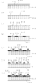
도 2는 본 발명에 따른 태양전지의 제조방법의 일 예를 나타내는 도면이다.
도 3은 본 발명에 따른 태양전지의 이면구조의 일 형태를 나타내는 도면이다.
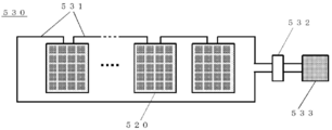
도 4는 본 발명에 따른 태양전지 모듈의 일 형태를 나타내는 도면이다.
도 5는 본 발명에 따른 태양광발전시스템의 일 형태를 나타내는 도면이다.
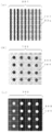
도 6은 종래의 이면전극형 태양전지의 기본구조를 나타내는 도면이다.

Claims (9)
- 결정 실리콘기판의 제1 주표면에, p형의 도전형을 갖는 p형 영역과, n형의 도전형을 갖는 n형 영역을 가지며, 상기 p형 영역 상에 형성된 양전극과, 상기 n형 영역 상에 형성된 음전극을 구비하는 이면전극형 태양전지로서,
상기 양전극이, 상기 p형 영역 상에 형성되고, III족원소를 포함하는 제1 도전체와, 이 제1 도전체 상에 적층되고, 상기 제1 도전체보다 III족원소의 함유비율이 낮은 제2 도전체와의 적층도전체로 이루어지는 것이며,
상기 음전극이, 상기 n형 영역 상에 형성된 상기 제2 도전체로 이루어지는 것을 특징으로 하는 태양전지. - 제1항에 있어서,
상기 제1 도전체가, 은을 주성분으로 하는 것을 특징으로 하는 태양전지. - 제1항에 있어서,
상기 제1 도전체가, 알루미늄을 주성분으로 하는 것을 특징으로 하는 태양전지. - 제1항 내지 제3항 중 어느 한 항에 있어서,
추가로, 상기 p형 영역과 상기 n형 영역의 상기 양전극 및 상기 음전극이 형성되어 있지 않은 표면에 형성된 패시베이션막을 구비하는 것을 특징으로 하는 태양전지. - 제1항 내지 제4항 중 어느 한 항에 기재된 태양전지를 전기적으로 접속하여 이루어지는 것을 특징으로 하는 태양전지 모듈.
- 제5항에 기재된 태양전지 모듈을 전기적으로 복수개 접속하여 이루어지는 것을 특징으로 하는 태양전지 발전시스템.
- 결정 실리콘기판의 제1 주표면에 p형의 도전형을 갖는 p형 영역 및 n형의 도전형을 갖는 n형 영역을 형성하는 공정과,
상기 p형 영역 상에 III족원소를 포함하는 제1 도전체를 형성하는 공정과,
이 제1 도전체 상과 상기 n형 영역 상의 양방에 상기 제1 도전체보다 III족원소의 함유비율이 낮은 제2 도전체를 형성하는 공정
을 포함하고,
상기 제1 도전체를 형성하는 공정과 상기 제2 도전체를 형성하는 공정에 의해, 상기 제1 도전체와 상기 제2 도전체의 적층도전체로 이루어지는 양전극과, 상기 제2 도전체로 이루어지는 음전극을 형성하는 것을 특징으로 하는 태양전지의 제조방법. - 제7항에 있어서,
상기 제1 도전체를 형성하는 공정과 상기 제2 도전체를 형성하는 공정은, 전극제를 스크린 인쇄 또는 디스펜싱 형성하는 스텝을 포함하는 것을 특징으로 하는 태양전지의 제조방법. - 제7항 또는 제8항에 있어서,
추가로, 상기 제1 도전체를 형성하는 공정과 상기 제2 도전체를 형성하는 공정보다 전에, 상기 p형 영역과 상기 n형 영역의 표면에 패시베이션막을 형성하는 공정을 포함하고,
상기 제1 도전체를 형성하는 공정에 있어서, 상기 패시베이션막을 개재하여 상기 p형 영역 상에 III족원소를 포함하는 상기 제1 전극제를 도포하고,
상기 제2 도전체를 형성하는 공정에 있어서, 이 제1 전극제 상과 상기 패시베이션막을 개재한 상기 n형 영역 상의 양방에 상기 제1 전극제보다 III족원소의 함유비율이 낮은 제2 전극제를 도포하고,
상기 제2 도전체를 형성하는 공정의 후에, 상기 제1 전극제와 상기 제2 전극제를 소결함으로써, 상기 양전극과 상기 음전극을 형성하는 것을 특징으로 하는 태양전지의 제조방법.
Applications Claiming Priority (3)
| Application Number | Priority Date | Filing Date | Title |
|---|---|---|---|
| JP2017124479A JP6741626B2 (ja) | 2017-06-26 | 2017-06-26 | 高効率裏面電極型太陽電池及びその製造方法 |
| JPJP-P-2017-124479 | 2017-06-26 | ||
| PCT/JP2018/017615 WO2019003638A1 (ja) | 2017-06-26 | 2018-05-07 | 高効率裏面電極型太陽電池及びその製造方法 |
Publications (2)
| Publication Number | Publication Date |
|---|---|
| KR20200023301A true KR20200023301A (ko) | 2020-03-04 |
| KR102563642B1 KR102563642B1 (ko) | 2023-08-04 |
Family
ID=64741452
Family Applications (1)
| Application Number | Title | Priority Date | Filing Date |
|---|---|---|---|
| KR1020197038090A Active KR102563642B1 (ko) | 2017-06-26 | 2018-05-07 | 고효율 이면전극형 태양전지 및 그 제조방법 |
Country Status (9)
| Country | Link |
|---|---|
| US (1) | US11984522B2 (ko) |
| EP (1) | EP3648175B1 (ko) |
| JP (1) | JP6741626B2 (ko) |
| KR (1) | KR102563642B1 (ko) |
| CN (1) | CN110800114B (ko) |
| ES (1) | ES2942985T3 (ko) |
| MY (1) | MY201464A (ko) |
| TW (1) | TWI753179B (ko) |
| WO (1) | WO2019003638A1 (ko) |
Families Citing this family (1)
| Publication number | Priority date | Publication date | Assignee | Title |
|---|---|---|---|---|
| CN117153951B (zh) * | 2023-10-20 | 2024-07-19 | 正泰新能科技股份有限公司 | 一种背接触光伏组件的生产方法及背接触光伏组件 |
Citations (8)
| Publication number | Priority date | Publication date | Assignee | Title |
|---|---|---|---|---|
| JPS6159546A (ja) | 1984-08-30 | 1986-03-27 | Fujitsu Ltd | リカバリ・デ−タ制御方式 |
| JP2002511190A (ja) | 1997-05-06 | 2002-04-09 | エバラ・ソーラー・インコーポレーテッド | シリコン太陽電池および他のデバイス用の自己ドーピング陰極および陽極のための方法および装置 |
| JP2004179334A (ja) * | 2002-11-26 | 2004-06-24 | Kyocera Corp | 太陽電池素子の形成方法 |
| CN101383386A (zh) * | 2008-10-24 | 2009-03-11 | 中国科学院电工研究所 | 一种发射极环绕型太阳电池及其制备方法 |
| KR20120102590A (ko) * | 2009-12-18 | 2012-09-18 | 도레이 카부시키가이샤 | 반도체 디바이스의 제조 방법 및 이면 접합형 태양 전지 |
| US20140210073A1 (en) * | 2011-08-31 | 2014-07-31 | Sharp Kabushiki Kaisha | Conductive paste, electrode for semiconductor device, semiconductor device, and method for manufacturing semiconductor device |
| KR20150040830A (ko) * | 2015-03-26 | 2015-04-15 | 주식회사 엘지화학 | 식각 마스크 페이스트 및 이를 이용한 후면전극형 태양전지 |
| KR20150053551A (ko) * | 2013-11-08 | 2015-05-18 | 엘지전자 주식회사 | 태양 전지 |
Family Cites Families (37)
| Publication number | Priority date | Publication date | Assignee | Title |
|---|---|---|---|---|
| JPS5426674A (en) | 1977-07-29 | 1979-02-28 | Matsushita Electric Ind Co Ltd | Electrode material for semiconductor device |
| US8309844B2 (en) * | 2007-08-29 | 2012-11-13 | Ferro Corporation | Thick film pastes for fire through applications in solar cells |
| EP2417607A1 (en) * | 2009-04-08 | 2012-02-15 | E. I. du Pont de Nemours and Company | Solar cell electrode |
| KR20120104431A (ko) * | 2010-01-22 | 2012-09-20 | 샤프 가부시키가이샤 | 이면 전극형 태양전지 셀, 배선 시트, 배선 시트를 가진 태양전지 셀, 태양전지 모듈 및 배선 시트를 가진 태양전지 셀의 제조방법 |
| WO2011163534A1 (en) * | 2010-06-24 | 2011-12-29 | E. I. Du Pont De Nemours And Company | Process for the formation of a silver back anode of a silicon solar cell |
| JP5642591B2 (ja) * | 2011-02-28 | 2014-12-17 | 三洋電機株式会社 | 太陽電池モジュール |
| US20120222721A1 (en) * | 2011-03-02 | 2012-09-06 | General Electric Company | Photovoltaic module package and fabrication method |
| KR20120113548A (ko) | 2011-04-05 | 2012-10-15 | 주식회사 엘지화학 | 식각 마스크 페이스트 및 이를 이용한 후면전극형 태양전지 |
| US20140360567A1 (en) * | 2011-08-05 | 2014-12-11 | Solexel, Inc. | Back contact solar cells using aluminum-based alloy metallization |
| US20130288425A1 (en) * | 2011-08-05 | 2013-10-31 | Solexel, Inc. | End point detection for back contact solar cell laser via drilling |
| US20130042912A1 (en) * | 2011-08-12 | 2013-02-21 | Hitachi Chemical Company, Ltd. | Solder bonded body, method of producing solder bonded body, element, photovoltaic cell, method of producing element and method of producing photovoltaic cell |
| WO2013036510A1 (en) * | 2011-09-09 | 2013-03-14 | Ferro Corporation | Silver solar cell contacts |
| KR20130050721A (ko) * | 2011-11-08 | 2013-05-16 | 삼성에스디아이 주식회사 | 태양 전지 |
| KR101863294B1 (ko) * | 2011-11-25 | 2018-05-31 | 인텔렉츄얼 키스톤 테크놀로지 엘엘씨 | 태양전지 및 그 제조 방법 |
| KR101356849B1 (ko) * | 2012-03-15 | 2014-02-03 | 고려대학교 산학협력단 | 결정질 실리콘 태양 전지 및 이의 제조방법 |
| TW201340347A (zh) * | 2012-03-22 | 2013-10-01 | Motech Ind Inc | 太陽能電池 |
| KR101387718B1 (ko) * | 2012-05-07 | 2014-04-22 | 엘지전자 주식회사 | 태양 전지 및 이의 제조 방법 |
| JP2014029963A (ja) * | 2012-07-31 | 2014-02-13 | Panasonic Corp | 太陽電池モジュール |
| CN103151395A (zh) * | 2013-01-25 | 2013-06-12 | 友达光电股份有限公司 | 太阳能电池 |
| JP6141223B2 (ja) * | 2013-06-14 | 2017-06-07 | 三菱電機株式会社 | 受光素子モジュールおよびその製造方法 |
| WO2015060432A1 (ja) * | 2013-10-25 | 2015-04-30 | シャープ株式会社 | 光電変換装置 |
| KR101620431B1 (ko) * | 2014-01-29 | 2016-05-12 | 엘지전자 주식회사 | 태양 전지 및 이의 제조 방법 |
| KR102175893B1 (ko) * | 2014-02-24 | 2020-11-06 | 엘지전자 주식회사 | 태양 전지 모듈의 제조 방법 |
| KR101867855B1 (ko) * | 2014-03-17 | 2018-06-15 | 엘지전자 주식회사 | 태양 전지 |
| JP2015177175A (ja) * | 2014-03-18 | 2015-10-05 | シャープ株式会社 | 光電変換素子および光電変換素子の製造方法 |
| US9349883B2 (en) * | 2014-06-19 | 2016-05-24 | E I Du Pont De Nemours And Company | Conductor for a solar cell |
| WO2016028825A1 (en) * | 2014-08-18 | 2016-02-25 | Solexel, Inc. | Photovoltaic solar module metallization and distributed shade management connection and fabrication methods |
| JP2015188089A (ja) * | 2015-04-30 | 2015-10-29 | 日立化成株式会社 | 素子及び太陽電池 |
| US10217877B2 (en) * | 2015-07-27 | 2019-02-26 | Lg Electronics Inc. | Solar cell |
| EP3340315B1 (en) * | 2015-08-21 | 2021-10-27 | Sharp Kabushiki Kaisha | Photoelectric conversion element |
| KR20170028548A (ko) * | 2015-09-04 | 2017-03-14 | 엘지전자 주식회사 | 태양 전지 모듈 |
| JP6598608B2 (ja) | 2015-09-10 | 2019-10-30 | ホーチキ株式会社 | 消火栓装置 |
| US20180212072A1 (en) * | 2015-09-25 | 2018-07-26 | Mitsubishi Electric Corporation | Manufacturing method for solar cell and solar cell |
| EP3151289A1 (en) * | 2015-10-01 | 2017-04-05 | LG Electronics Inc. | Solar cell |
| US11049988B2 (en) * | 2016-10-25 | 2021-06-29 | Shin-Etsu Chemical Co., Ltd. | High photoelectric conversion efficiency solar cell and method for manufacturing high photoelectric conversion efficiency solar cell |
| US11631779B2 (en) * | 2016-11-07 | 2023-04-18 | Shin-Etsu Chemical Co., Ltd. | Solar cell with high photoelectric conversion efficiency and method for manufacturing solar cell with high photoelectric conversion efficiency |
| EP3349251B1 (en) * | 2016-11-15 | 2020-04-22 | Shin-Etsu Chemical Co., Ltd | High efficiency solar cell and method for manufacturing high efficiency solar cell |
-
2017
- 2017-06-26 JP JP2017124479A patent/JP6741626B2/ja active Active
-
2018
- 2018-05-07 ES ES18825325T patent/ES2942985T3/es active Active
- 2018-05-07 CN CN201880043093.2A patent/CN110800114B/zh active Active
- 2018-05-07 US US16/623,872 patent/US11984522B2/en active Active
- 2018-05-07 EP EP18825325.6A patent/EP3648175B1/en active Active
- 2018-05-07 WO PCT/JP2018/017615 patent/WO2019003638A1/ja not_active Ceased
- 2018-05-07 MY MYPI2019007555A patent/MY201464A/en unknown
- 2018-05-07 KR KR1020197038090A patent/KR102563642B1/ko active Active
- 2018-06-22 TW TW107121409A patent/TWI753179B/zh active
Patent Citations (8)
| Publication number | Priority date | Publication date | Assignee | Title |
|---|---|---|---|---|
| JPS6159546A (ja) | 1984-08-30 | 1986-03-27 | Fujitsu Ltd | リカバリ・デ−タ制御方式 |
| JP2002511190A (ja) | 1997-05-06 | 2002-04-09 | エバラ・ソーラー・インコーポレーテッド | シリコン太陽電池および他のデバイス用の自己ドーピング陰極および陽極のための方法および装置 |
| JP2004179334A (ja) * | 2002-11-26 | 2004-06-24 | Kyocera Corp | 太陽電池素子の形成方法 |
| CN101383386A (zh) * | 2008-10-24 | 2009-03-11 | 中国科学院电工研究所 | 一种发射极环绕型太阳电池及其制备方法 |
| KR20120102590A (ko) * | 2009-12-18 | 2012-09-18 | 도레이 카부시키가이샤 | 반도체 디바이스의 제조 방법 및 이면 접합형 태양 전지 |
| US20140210073A1 (en) * | 2011-08-31 | 2014-07-31 | Sharp Kabushiki Kaisha | Conductive paste, electrode for semiconductor device, semiconductor device, and method for manufacturing semiconductor device |
| KR20150053551A (ko) * | 2013-11-08 | 2015-05-18 | 엘지전자 주식회사 | 태양 전지 |
| KR20150040830A (ko) * | 2015-03-26 | 2015-04-15 | 주식회사 엘지화학 | 식각 마스크 페이스트 및 이를 이용한 후면전극형 태양전지 |
Also Published As
| Publication number | Publication date |
|---|---|
| JP2019009312A (ja) | 2019-01-17 |
| CN110800114B (zh) | 2023-04-28 |
| MY201464A (en) | 2024-02-24 |
| EP3648175A1 (en) | 2020-05-06 |
| TWI753179B (zh) | 2022-01-21 |
| EP3648175B1 (en) | 2023-02-15 |
| TW201907450A (zh) | 2019-02-16 |
| WO2019003638A1 (ja) | 2019-01-03 |
| KR102563642B1 (ko) | 2023-08-04 |
| EP3648175A4 (en) | 2021-03-24 |
| US11984522B2 (en) | 2024-05-14 |
| JP6741626B2 (ja) | 2020-08-19 |
| ES2942985T3 (es) | 2023-06-08 |
| US20210143291A1 (en) | 2021-05-13 |
| CN110800114A (zh) | 2020-02-14 |
Similar Documents
| Publication | Publication Date | Title |
|---|---|---|
| JP6285545B2 (ja) | 太陽電池素子および太陽電池モジュール | |
| JP5490231B2 (ja) | 太陽電池素子およびその製造方法ならびに太陽電池モジュール | |
| WO2012133692A1 (ja) | 太陽電池素子および太陽電池モジュール | |
| US20170133545A1 (en) | Passivated contacts for photovoltaic cells | |
| WO2013002285A1 (ja) | アルミナ膜の形成方法および太陽電池素子 | |
| JP2014011246A (ja) | 太陽電池素子および太陽電池モジュール | |
| WO2013100085A1 (ja) | 太陽電池素子、太陽電池素子の製造方法および太陽電池モジュール | |
| KR102674774B1 (ko) | 고광전변환효율 태양전지 및 고광전변환효율 태양전지의 제조 방법 | |
| JP6688244B2 (ja) | 高効率太陽電池の製造方法及び太陽電池セルの製造システム | |
| JP6430842B2 (ja) | 太陽電池素子の製造方法および太陽電池モジュールの製造方法 | |
| CN109041583B (zh) | 太阳能电池元件以及太阳能电池模块 | |
| KR20110045979A (ko) | 태양 전지 및 그 제조 방법 | |
| KR102563642B1 (ko) | 고효율 이면전극형 태양전지 및 그 제조방법 | |
| KR100995654B1 (ko) | 태양전지 및 그 제조방법 | |
| KR101151413B1 (ko) | 이중 반사 방지막을 갖는 태양 전지 및 그 제조 방법 | |
| WO2017057618A1 (ja) | 太陽電池素子およびその製造方法並びに太陽電池モジュール |
Legal Events
| Date | Code | Title | Description |
|---|---|---|---|
| PA0105 | International application |
Patent event date: 20191224 Patent event code: PA01051R01D Comment text: International Patent Application |
|
| PG1501 | Laying open of application | ||
| PA0201 | Request for examination |
Patent event code: PA02012R01D Patent event date: 20210412 Comment text: Request for Examination of Application |
|
| E902 | Notification of reason for refusal | ||
| PE0902 | Notice of grounds for rejection |
Comment text: Notification of reason for refusal Patent event date: 20230421 Patent event code: PE09021S01D |
|
| E701 | Decision to grant or registration of patent right | ||
| PE0701 | Decision of registration |
Patent event code: PE07011S01D Comment text: Decision to Grant Registration Patent event date: 20230623 |
|
| GRNT | Written decision to grant | ||
| PR0701 | Registration of establishment |
Comment text: Registration of Establishment Patent event date: 20230801 Patent event code: PR07011E01D |
|
| PR1002 | Payment of registration fee |
Payment date: 20230802 End annual number: 3 Start annual number: 1 |
|
| PG1601 | Publication of registration |