KR20200025091A - 게이트 드라이버, 유기발광표시장치 및 그의 구동방법 - Google Patents
게이트 드라이버, 유기발광표시장치 및 그의 구동방법 Download PDFInfo
- Publication number
- KR20200025091A KR20200025091A KR1020180101931A KR20180101931A KR20200025091A KR 20200025091 A KR20200025091 A KR 20200025091A KR 1020180101931 A KR1020180101931 A KR 1020180101931A KR 20180101931 A KR20180101931 A KR 20180101931A KR 20200025091 A KR20200025091 A KR 20200025091A
- Authority
- KR
- South Korea
- Prior art keywords
- potential voltage
- low potential
- voltage
- signal
- gate
- Prior art date
- Legal status (The legal status is an assumption and is not a legal conclusion. Google has not performed a legal analysis and makes no representation as to the accuracy of the status listed.)
- Granted
Links
Images





Classifications
-
- G—PHYSICS
- G09—EDUCATION; CRYPTOGRAPHY; DISPLAY; ADVERTISING; SEALS
- G09G—ARRANGEMENTS OR CIRCUITS FOR CONTROL OF INDICATING DEVICES USING STATIC MEANS TO PRESENT VARIABLE INFORMATION
- G09G3/00—Control arrangements or circuits, of interest only in connection with visual indicators other than cathode-ray tubes
- G09G3/20—Control arrangements or circuits, of interest only in connection with visual indicators other than cathode-ray tubes for presentation of an assembly of a number of characters, e.g. a page, by composing the assembly by combination of individual elements arranged in a matrix no fixed position being assigned to or needed to be assigned to the individual characters or partial characters
- G09G3/22—Control arrangements or circuits, of interest only in connection with visual indicators other than cathode-ray tubes for presentation of an assembly of a number of characters, e.g. a page, by composing the assembly by combination of individual elements arranged in a matrix no fixed position being assigned to or needed to be assigned to the individual characters or partial characters using controlled light sources
- G09G3/30—Control arrangements or circuits, of interest only in connection with visual indicators other than cathode-ray tubes for presentation of an assembly of a number of characters, e.g. a page, by composing the assembly by combination of individual elements arranged in a matrix no fixed position being assigned to or needed to be assigned to the individual characters or partial characters using controlled light sources using electroluminescent panels
- G09G3/32—Control arrangements or circuits, of interest only in connection with visual indicators other than cathode-ray tubes for presentation of an assembly of a number of characters, e.g. a page, by composing the assembly by combination of individual elements arranged in a matrix no fixed position being assigned to or needed to be assigned to the individual characters or partial characters using controlled light sources using electroluminescent panels semiconductive, e.g. using light-emitting diodes [LED]
- G09G3/3208—Control arrangements or circuits, of interest only in connection with visual indicators other than cathode-ray tubes for presentation of an assembly of a number of characters, e.g. a page, by composing the assembly by combination of individual elements arranged in a matrix no fixed position being assigned to or needed to be assigned to the individual characters or partial characters using controlled light sources using electroluminescent panels semiconductive, e.g. using light-emitting diodes [LED] organic, e.g. using organic light-emitting diodes [OLED]
-
- G—PHYSICS
- G09—EDUCATION; CRYPTOGRAPHY; DISPLAY; ADVERTISING; SEALS
- G09G—ARRANGEMENTS OR CIRCUITS FOR CONTROL OF INDICATING DEVICES USING STATIC MEANS TO PRESENT VARIABLE INFORMATION
- G09G3/00—Control arrangements or circuits, of interest only in connection with visual indicators other than cathode-ray tubes
- G09G3/20—Control arrangements or circuits, of interest only in connection with visual indicators other than cathode-ray tubes for presentation of an assembly of a number of characters, e.g. a page, by composing the assembly by combination of individual elements arranged in a matrix no fixed position being assigned to or needed to be assigned to the individual characters or partial characters
- G09G3/22—Control arrangements or circuits, of interest only in connection with visual indicators other than cathode-ray tubes for presentation of an assembly of a number of characters, e.g. a page, by composing the assembly by combination of individual elements arranged in a matrix no fixed position being assigned to or needed to be assigned to the individual characters or partial characters using controlled light sources
- G09G3/30—Control arrangements or circuits, of interest only in connection with visual indicators other than cathode-ray tubes for presentation of an assembly of a number of characters, e.g. a page, by composing the assembly by combination of individual elements arranged in a matrix no fixed position being assigned to or needed to be assigned to the individual characters or partial characters using controlled light sources using electroluminescent panels
- G09G3/32—Control arrangements or circuits, of interest only in connection with visual indicators other than cathode-ray tubes for presentation of an assembly of a number of characters, e.g. a page, by composing the assembly by combination of individual elements arranged in a matrix no fixed position being assigned to or needed to be assigned to the individual characters or partial characters using controlled light sources using electroluminescent panels semiconductive, e.g. using light-emitting diodes [LED]
- G09G3/3208—Control arrangements or circuits, of interest only in connection with visual indicators other than cathode-ray tubes for presentation of an assembly of a number of characters, e.g. a page, by composing the assembly by combination of individual elements arranged in a matrix no fixed position being assigned to or needed to be assigned to the individual characters or partial characters using controlled light sources using electroluminescent panels semiconductive, e.g. using light-emitting diodes [LED] organic, e.g. using organic light-emitting diodes [OLED]
- G09G3/3225—Control arrangements or circuits, of interest only in connection with visual indicators other than cathode-ray tubes for presentation of an assembly of a number of characters, e.g. a page, by composing the assembly by combination of individual elements arranged in a matrix no fixed position being assigned to or needed to be assigned to the individual characters or partial characters using controlled light sources using electroluminescent panels semiconductive, e.g. using light-emitting diodes [LED] organic, e.g. using organic light-emitting diodes [OLED] using an active matrix
- G09G3/3258—Control arrangements or circuits, of interest only in connection with visual indicators other than cathode-ray tubes for presentation of an assembly of a number of characters, e.g. a page, by composing the assembly by combination of individual elements arranged in a matrix no fixed position being assigned to or needed to be assigned to the individual characters or partial characters using controlled light sources using electroluminescent panels semiconductive, e.g. using light-emitting diodes [LED] organic, e.g. using organic light-emitting diodes [OLED] using an active matrix with pixel circuitry controlling the voltage across the light-emitting element
-
- G—PHYSICS
- G09—EDUCATION; CRYPTOGRAPHY; DISPLAY; ADVERTISING; SEALS
- G09G—ARRANGEMENTS OR CIRCUITS FOR CONTROL OF INDICATING DEVICES USING STATIC MEANS TO PRESENT VARIABLE INFORMATION
- G09G3/00—Control arrangements or circuits, of interest only in connection with visual indicators other than cathode-ray tubes
- G09G3/20—Control arrangements or circuits, of interest only in connection with visual indicators other than cathode-ray tubes for presentation of an assembly of a number of characters, e.g. a page, by composing the assembly by combination of individual elements arranged in a matrix no fixed position being assigned to or needed to be assigned to the individual characters or partial characters
- G09G3/22—Control arrangements or circuits, of interest only in connection with visual indicators other than cathode-ray tubes for presentation of an assembly of a number of characters, e.g. a page, by composing the assembly by combination of individual elements arranged in a matrix no fixed position being assigned to or needed to be assigned to the individual characters or partial characters using controlled light sources
- G09G3/30—Control arrangements or circuits, of interest only in connection with visual indicators other than cathode-ray tubes for presentation of an assembly of a number of characters, e.g. a page, by composing the assembly by combination of individual elements arranged in a matrix no fixed position being assigned to or needed to be assigned to the individual characters or partial characters using controlled light sources using electroluminescent panels
- G09G3/32—Control arrangements or circuits, of interest only in connection with visual indicators other than cathode-ray tubes for presentation of an assembly of a number of characters, e.g. a page, by composing the assembly by combination of individual elements arranged in a matrix no fixed position being assigned to or needed to be assigned to the individual characters or partial characters using controlled light sources using electroluminescent panels semiconductive, e.g. using light-emitting diodes [LED]
- G09G3/3208—Control arrangements or circuits, of interest only in connection with visual indicators other than cathode-ray tubes for presentation of an assembly of a number of characters, e.g. a page, by composing the assembly by combination of individual elements arranged in a matrix no fixed position being assigned to or needed to be assigned to the individual characters or partial characters using controlled light sources using electroluminescent panels semiconductive, e.g. using light-emitting diodes [LED] organic, e.g. using organic light-emitting diodes [OLED]
- G09G3/3266—Details of drivers for scan electrodes
-
- G—PHYSICS
- G06—COMPUTING OR CALCULATING; COUNTING
- G06F—ELECTRIC DIGITAL DATA PROCESSING
- G06F1/00—Details not covered by groups G06F3/00 - G06F13/00 and G06F21/00
- G06F1/04—Generating or distributing clock signals or signals derived directly therefrom
-
- G—PHYSICS
- G09—EDUCATION; CRYPTOGRAPHY; DISPLAY; ADVERTISING; SEALS
- G09G—ARRANGEMENTS OR CIRCUITS FOR CONTROL OF INDICATING DEVICES USING STATIC MEANS TO PRESENT VARIABLE INFORMATION
- G09G3/00—Control arrangements or circuits, of interest only in connection with visual indicators other than cathode-ray tubes
- G09G3/20—Control arrangements or circuits, of interest only in connection with visual indicators other than cathode-ray tubes for presentation of an assembly of a number of characters, e.g. a page, by composing the assembly by combination of individual elements arranged in a matrix no fixed position being assigned to or needed to be assigned to the individual characters or partial characters
- G09G3/22—Control arrangements or circuits, of interest only in connection with visual indicators other than cathode-ray tubes for presentation of an assembly of a number of characters, e.g. a page, by composing the assembly by combination of individual elements arranged in a matrix no fixed position being assigned to or needed to be assigned to the individual characters or partial characters using controlled light sources
- G09G3/30—Control arrangements or circuits, of interest only in connection with visual indicators other than cathode-ray tubes for presentation of an assembly of a number of characters, e.g. a page, by composing the assembly by combination of individual elements arranged in a matrix no fixed position being assigned to or needed to be assigned to the individual characters or partial characters using controlled light sources using electroluminescent panels
- G09G3/32—Control arrangements or circuits, of interest only in connection with visual indicators other than cathode-ray tubes for presentation of an assembly of a number of characters, e.g. a page, by composing the assembly by combination of individual elements arranged in a matrix no fixed position being assigned to or needed to be assigned to the individual characters or partial characters using controlled light sources using electroluminescent panels semiconductive, e.g. using light-emitting diodes [LED]
- G09G3/3208—Control arrangements or circuits, of interest only in connection with visual indicators other than cathode-ray tubes for presentation of an assembly of a number of characters, e.g. a page, by composing the assembly by combination of individual elements arranged in a matrix no fixed position being assigned to or needed to be assigned to the individual characters or partial characters using controlled light sources using electroluminescent panels semiconductive, e.g. using light-emitting diodes [LED] organic, e.g. using organic light-emitting diodes [OLED]
- G09G3/3225—Control arrangements or circuits, of interest only in connection with visual indicators other than cathode-ray tubes for presentation of an assembly of a number of characters, e.g. a page, by composing the assembly by combination of individual elements arranged in a matrix no fixed position being assigned to or needed to be assigned to the individual characters or partial characters using controlled light sources using electroluminescent panels semiconductive, e.g. using light-emitting diodes [LED] organic, e.g. using organic light-emitting diodes [OLED] using an active matrix
-
- G—PHYSICS
- G09—EDUCATION; CRYPTOGRAPHY; DISPLAY; ADVERTISING; SEALS
- G09G—ARRANGEMENTS OR CIRCUITS FOR CONTROL OF INDICATING DEVICES USING STATIC MEANS TO PRESENT VARIABLE INFORMATION
- G09G3/00—Control arrangements or circuits, of interest only in connection with visual indicators other than cathode-ray tubes
- G09G3/20—Control arrangements or circuits, of interest only in connection with visual indicators other than cathode-ray tubes for presentation of an assembly of a number of characters, e.g. a page, by composing the assembly by combination of individual elements arranged in a matrix no fixed position being assigned to or needed to be assigned to the individual characters or partial characters
- G09G3/22—Control arrangements or circuits, of interest only in connection with visual indicators other than cathode-ray tubes for presentation of an assembly of a number of characters, e.g. a page, by composing the assembly by combination of individual elements arranged in a matrix no fixed position being assigned to or needed to be assigned to the individual characters or partial characters using controlled light sources
- G09G3/30—Control arrangements or circuits, of interest only in connection with visual indicators other than cathode-ray tubes for presentation of an assembly of a number of characters, e.g. a page, by composing the assembly by combination of individual elements arranged in a matrix no fixed position being assigned to or needed to be assigned to the individual characters or partial characters using controlled light sources using electroluminescent panels
- G09G3/32—Control arrangements or circuits, of interest only in connection with visual indicators other than cathode-ray tubes for presentation of an assembly of a number of characters, e.g. a page, by composing the assembly by combination of individual elements arranged in a matrix no fixed position being assigned to or needed to be assigned to the individual characters or partial characters using controlled light sources using electroluminescent panels semiconductive, e.g. using light-emitting diodes [LED]
- G09G3/3208—Control arrangements or circuits, of interest only in connection with visual indicators other than cathode-ray tubes for presentation of an assembly of a number of characters, e.g. a page, by composing the assembly by combination of individual elements arranged in a matrix no fixed position being assigned to or needed to be assigned to the individual characters or partial characters using controlled light sources using electroluminescent panels semiconductive, e.g. using light-emitting diodes [LED] organic, e.g. using organic light-emitting diodes [OLED]
- G09G3/3275—Details of drivers for data electrodes
- G09G3/3291—Details of drivers for data electrodes in which the data driver supplies a variable data voltage for setting the current through, or the voltage across, the light-emitting elements
-
- G—PHYSICS
- G09—EDUCATION; CRYPTOGRAPHY; DISPLAY; ADVERTISING; SEALS
- G09G—ARRANGEMENTS OR CIRCUITS FOR CONTROL OF INDICATING DEVICES USING STATIC MEANS TO PRESENT VARIABLE INFORMATION
- G09G2300/00—Aspects of the constitution of display devices
- G09G2300/04—Structural and physical details of display devices
- G09G2300/0421—Structural details of the set of electrodes
- G09G2300/043—Compensation electrodes or other additional electrodes in matrix displays related to distortions or compensation signals, e.g. for modifying TFT threshold voltage in column driver
-
- G—PHYSICS
- G09—EDUCATION; CRYPTOGRAPHY; DISPLAY; ADVERTISING; SEALS
- G09G—ARRANGEMENTS OR CIRCUITS FOR CONTROL OF INDICATING DEVICES USING STATIC MEANS TO PRESENT VARIABLE INFORMATION
- G09G2300/00—Aspects of the constitution of display devices
- G09G2300/08—Active matrix structure, i.e. with use of active elements, inclusive of non-linear two terminal elements, in the pixels together with light emitting or modulating elements
- G09G2300/0809—Several active elements per pixel in active matrix panels
- G09G2300/0819—Several active elements per pixel in active matrix panels used for counteracting undesired variations, e.g. feedback or autozeroing
-
- G—PHYSICS
- G09—EDUCATION; CRYPTOGRAPHY; DISPLAY; ADVERTISING; SEALS
- G09G—ARRANGEMENTS OR CIRCUITS FOR CONTROL OF INDICATING DEVICES USING STATIC MEANS TO PRESENT VARIABLE INFORMATION
- G09G2300/00—Aspects of the constitution of display devices
- G09G2300/08—Active matrix structure, i.e. with use of active elements, inclusive of non-linear two terminal elements, in the pixels together with light emitting or modulating elements
- G09G2300/0809—Several active elements per pixel in active matrix panels
- G09G2300/0842—Several active elements per pixel in active matrix panels forming a memory circuit, e.g. a dynamic memory with one capacitor
-
- G—PHYSICS
- G09—EDUCATION; CRYPTOGRAPHY; DISPLAY; ADVERTISING; SEALS
- G09G—ARRANGEMENTS OR CIRCUITS FOR CONTROL OF INDICATING DEVICES USING STATIC MEANS TO PRESENT VARIABLE INFORMATION
- G09G2310/00—Command of the display device
- G09G2310/02—Addressing, scanning or driving the display screen or processing steps related thereto
- G09G2310/0264—Details of driving circuits
- G09G2310/0289—Details of voltage level shifters arranged for use in a driving circuit
-
- G—PHYSICS
- G09—EDUCATION; CRYPTOGRAPHY; DISPLAY; ADVERTISING; SEALS
- G09G—ARRANGEMENTS OR CIRCUITS FOR CONTROL OF INDICATING DEVICES USING STATIC MEANS TO PRESENT VARIABLE INFORMATION
- G09G2310/00—Command of the display device
- G09G2310/06—Details of flat display driving waveforms
-
- G—PHYSICS
- G09—EDUCATION; CRYPTOGRAPHY; DISPLAY; ADVERTISING; SEALS
- G09G—ARRANGEMENTS OR CIRCUITS FOR CONTROL OF INDICATING DEVICES USING STATIC MEANS TO PRESENT VARIABLE INFORMATION
- G09G2310/00—Command of the display device
- G09G2310/06—Details of flat display driving waveforms
- G09G2310/067—Special waveforms for scanning, where no circuit details of the gate driver are given
-
- G—PHYSICS
- G09—EDUCATION; CRYPTOGRAPHY; DISPLAY; ADVERTISING; SEALS
- G09G—ARRANGEMENTS OR CIRCUITS FOR CONTROL OF INDICATING DEVICES USING STATIC MEANS TO PRESENT VARIABLE INFORMATION
- G09G2310/00—Command of the display device
- G09G2310/08—Details of timing specific for flat panels, other than clock recovery
-
- G—PHYSICS
- G09—EDUCATION; CRYPTOGRAPHY; DISPLAY; ADVERTISING; SEALS
- G09G—ARRANGEMENTS OR CIRCUITS FOR CONTROL OF INDICATING DEVICES USING STATIC MEANS TO PRESENT VARIABLE INFORMATION
- G09G2320/00—Control of display operating conditions
- G09G2320/02—Improving the quality of display appearance
-
- G—PHYSICS
- G09—EDUCATION; CRYPTOGRAPHY; DISPLAY; ADVERTISING; SEALS
- G09G—ARRANGEMENTS OR CIRCUITS FOR CONTROL OF INDICATING DEVICES USING STATIC MEANS TO PRESENT VARIABLE INFORMATION
- G09G2320/00—Control of display operating conditions
- G09G2320/02—Improving the quality of display appearance
- G09G2320/0223—Compensation for problems related to R-C delay and attenuation in electrodes of matrix panels, e.g. in gate electrodes or on-substrate video signal electrodes
-
- G—PHYSICS
- G09—EDUCATION; CRYPTOGRAPHY; DISPLAY; ADVERTISING; SEALS
- G09G—ARRANGEMENTS OR CIRCUITS FOR CONTROL OF INDICATING DEVICES USING STATIC MEANS TO PRESENT VARIABLE INFORMATION
- G09G2320/00—Control of display operating conditions
- G09G2320/02—Improving the quality of display appearance
- G09G2320/0257—Reduction of after-image effects
-
- G—PHYSICS
- G09—EDUCATION; CRYPTOGRAPHY; DISPLAY; ADVERTISING; SEALS
- G09G—ARRANGEMENTS OR CIRCUITS FOR CONTROL OF INDICATING DEVICES USING STATIC MEANS TO PRESENT VARIABLE INFORMATION
- G09G2320/00—Control of display operating conditions
- G09G2320/04—Maintaining the quality of display appearance
- G09G2320/043—Preventing or counteracting the effects of ageing
-
- G—PHYSICS
- G09—EDUCATION; CRYPTOGRAPHY; DISPLAY; ADVERTISING; SEALS
- G09G—ARRANGEMENTS OR CIRCUITS FOR CONTROL OF INDICATING DEVICES USING STATIC MEANS TO PRESENT VARIABLE INFORMATION
- G09G2330/00—Aspects of power supply; Aspects of display protection and defect management
- G09G2330/02—Details of power systems and of start or stop of display operation
- G09G2330/028—Generation of voltages supplied to electrode drivers in a matrix display other than LCD
Landscapes
- Engineering & Computer Science (AREA)
- Theoretical Computer Science (AREA)
- Physics & Mathematics (AREA)
- General Physics & Mathematics (AREA)
- Computer Hardware Design (AREA)
- General Engineering & Computer Science (AREA)
- Control Of Indicators Other Than Cathode Ray Tubes (AREA)
- Control Of El Displays (AREA)
- Electroluminescent Light Sources (AREA)
Abstract
Description
도 2는 도 1에 도시된 서브픽셀의 일 실시예를 나타내는 회로도이다.
도 3은 도 1에도시된 게이트드라이버와 전원부의 관계를 나타내는 구조도이다.
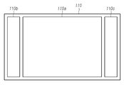
도 4는 도 1에 도시된 표시패널의 일 예를 나타내는 평면도이다.
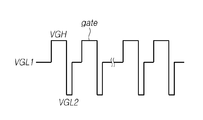
도 5a는 제1모드동안 레벨쉬프터에서 출력되는 신호를 나타내는 파형도이다.
도 5b는 제1모드동안 게이트신호생성회로에서 출력되는 게이트신호를 나타내는 파형도이다.
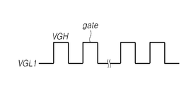
도 6a는 제2모드동안 레벨쉬프터에서 출력되는 신호를 나타내는 파형도이다.
도 6b는 제2모드동안 게이트신호생성회로에서 출력되는 게이트신호를 나타내는 파형도이다.
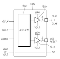
도 7은 도 3에 도시된 레벨쉬프터의 일 실시예를 나타내는 개념도이다.
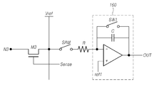
도 8은 도 2에 도시된 서브픽셀에 전류센싱부가 연결된 것을 나타내는 회로도이다.
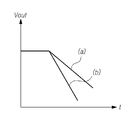
도 9는 도 8에 도시된 전류센싱부에서 센싱되는 전류를 나타내는 그래프이다.
도 10은 본 발명에 따른 유기발광표시장치의 구동방법의 일 실시예를 나타내는 순서도이다.

101: 서브픽셀
110: 표시패널
120: 게이트드라이버
130: 데이터드라이버
140: 타이밍컨트롤러
150: 전원부
Claims (17)
- 제1저전위전압과, 상기 제1저전위전압보다 전압레벨이 낮은 제2저전위전압을 전달받고 상기 제1저전위전압과 상기 제2저전위전압 중 하나의 전압을 선택하고 출력하되, 모드선택신호에 대응하여 제1모드에서는 상기 제1저전위전압을 선택하고 제2모드에서는 상기 제2저전위전압을 출력하는 선택부; 및
고전위전압과 상기 제1저전위전압을 전달받아 상기 고전위전압과 상기 제1저전위전압 사이의 전압레벨을 갖는 클럭신호를 출력하는 제1출력단과, 상기 선택부에서 선택된 상기 제1저전위전압 또는 상기 제2저전위전압에 대응하는 직류신호를 출력하는 제2출력단을 구비하는 레벨쉬프터를 포함하는 게이트드라이버.
- 제1항에 있어서,
상기 클럭신호와 상기 직류신호를 전달받아 게이트신호를 출력하되, 상기 제1모드에서 상기 게이트신호의 전압레벨을 상기 고전위전압과 상기 제1저전위전압을 반복되게 하고, 상기 제2모드에서 상기 게이트신호의 전압레벨을 상기 고전위전압, 상기 제2저전위전압, 제1저전위전압, 상기 고저전위전압의 순서로 변경되어 출력되게 하는 게이트신호생성회로를 포함하는 게이트드라이버.
- 제2항에 있어서,
상기 레벨쉬프터는 제어로직;
상기 제어로직에 의해 제어되고 상기 고전위전압, 상기 제1저전위전압을 이용하여 상기 클럭신호를 출력하는 클럭신호생성부; 및
상기 제어로직에 의해 제어되어 상기 게이트신호생성회로를 제어하는 제어신호생성부를 포함할 수 있다.
- 제1항에 있어서,
상기 모드선택신호를 타이밍 컨트롤러로부터 전달받되, 상기 타이밍 컨트롤러는 상기 제1모드에서 센싱신호를 출력하고, 상기 제2모드에서 영상신호를 출력하는 구동회로.
- 복수의 데이터라인과 복수의 게이트라인이 교차하며, 상기 복수의 데이터라인과 상기 복수의 게이트라인이 교차하는 영역에 정의되는 복수의 서브픽셀을 포함하는 표시패널;
상기 데이터라인에 데이터신호 또는 센싱신호를 전달다는 데이터드라이버;
상기 게이트라인에 게이트신호를 전달하는 게이트드라이버; 및
상기 데이터드라이버 및 상기 게이트드라이버를 제어하는 타이밍 컨트롤러를 포함하되,
상기 게이트드라이버는
제1저전위전압과, 상기 제1저전위전압보다 전압레벨이 낮은 제2저전위전압을 전달받고 상기 제1저전위전압과 상기 제2저전위전압 중 하나의 전압을 선택하고 출력하되, 모드선택신호에 대응하여 제1모드에서는 상기 제1저전위전압을 선택하고 제2모드에서는 상기 제2저전위전압을 출력하는 선택부; 및
고전위전압과 상기 제1저전위전압을 전달받아 상기 고전위전압과 상기 제1저전위전압 사이의 전압레벨을 갖는 펄스신호를 출력하는 제1출력단과, 상기 선택부에서 선택된 상기 제1저전위전압 또는 상기 제2저전위전압에 대응하는 직류신호를 출력하는 제2출력단을 구비하는 레벨쉬프터를 포함하는 유기발광표시장치.
- 제5항에 있어서,
상기 게이트드라이버는 상기 클럭신호와 상기 직류신호를 전달받아 게이트신호를 출력하되, 상기 제1모드에서 상기 게이트신호의 전압레벨을 상기 고전위전압과 상기 제1저전위전압을 반복되게 하고, 상기 제2모드에서 상기 게이트신호의 전압레벨을 상기 고전위전압, 상기 제2저전위전압, 제1저전위전압, 상기 고저전위전압의 순서로 변경되어 출력되게 하는 게이트신호생성회로를 포함하는 유기발광표시장치.
- 제6항에 있어서,
상기 게이트신호생성회로는 상기 표시패널 상에 배치되어 상기 복수의 게이트라인과 연결되는 유기발광표시장치.
- 제6항에 있어서,
상기 레벨쉬프터는 제어로직;
상기 제어로직에 의해 제어되고 상기 고전위전압, 상기 제1저전위전압을 이용하여 상기 클럭신호를 출력하는 클럭신호생성부; 및
상기 제어로직에 의해 제어되어 상기 게이트신호생성회로를 제어하는 제어신호생성부를 포함할 수 있다.
- 제5항에 있어서,
상기 타이밍컨트롤러는 상기 제1모드에서 상기 데이터드라이버가 상기 데이터라인으로 센싱신호에 대응하는 센싱전압을 출력하도록 제어하고 상기 제2모드에서 상기 데이터드라이버가 상기 데이터라인으로 데이터신호에 대응하는 데이터전압을 출력하도록 제어하는 유기발광표시장치.
- 제5항에 있어서,
상기 각 서브픽셀은,
고전위전압이 전달되는 제1전원라인에 연결된 제1노드에 제1전극이 연결되고 제2노드에 게이트전극이 연결되며 제3노드에 제2전극이 연결되는 제1트랜지스터;
상기 데이터라인에 제1전극이 연결되고 상기 게이트라인에 게이트전극이 연결되며 상기 제2노드에 제2전극이 연결되는 제2트랜지스터;
상기 제3노드에 제1전극이 연결되고 센싱신호라인에 게이트전극이 연결되며 레퍼런스전압을 전달하는 제2전원라인에 제2전극이 연결되는 제3트랜지스터;
상기 제1노드와 상기 제3노드 사이에 연결되는 캐패시터; 및
제1전극이 상기 제3노드에 연결되고 제2전극이 저전위전압에 연결되는 유기발광다이오드를 포함하는 유기발광표시장치.
- 제10항에 있어서,
상기 제3노드와 연결되는 전류센싱부를 포함하고, 상기 전류센싱부는 상기 제3노드에 흐르는 전류를 센싱하여 상기 서브픽셀의 특성값에 대응하는 정보를 출력하는 유기발광표시장치.
- 제11항에 있어서,
상기 전류센싱부는 적분기를 포함하고, 상기 적분기는 상기 제3노드에 흐르는 전류에 의해 생성된 센싱전압과 기설정된 기준전압을 비교하여 상기 서브픽셀의 특성값에 대응하는 정보를 출력하는 유기발광표시장치.
- 제6항에 있어서,
상기 제1모드와 제2모드는 교번적으로 반복되는 유기발광표시장치.
- 제6항에 있어서,
상기 제1모드는 상기 표시패널의 구동이 시작될 때 수행되는 유기발광표시장치.
- 제1모드에서 게이트신호에 대응하여 센싱전압을 서브픽셀에 공급하는 단계; 및
제2모드에서 상기 게이트신호에 대응하여 데이터전압을 서브픽셀에 공급하는 단계;를 포함하되,
상기 제1모드에서 상기 게이트신호의 전압레벨은 제1저전위전압, 고전위 전압, 제2저전위전압, 제1저전위전압의 순서로 변경되고,
상기 제2모드에서 상기 게이트신호의 전압레벨은 상기 제1저전위전압, 상기 고전위전압을 반복하는 유기발광표시장치의 구동방법.
- 제15항에 있어서,
상기 제1모드에서 상기 고전위전압과 상기 제1저전위전압 사이의 전압레벨을 갖는 펄스신호와, 상기 제2저전위전압의 전압레벨을 갖는 직류신호를 전달받아 상기 게이트신호를 출력하는 유기발광표시장치.
- 제15항에 있어서,
상기 제2모드에서 상기 고전위전압과 상기 제1저전위전압 사이의 전압레벨을 갖는 펄스신호와, 상기 제1저전위전압의 전압레벨을 갖는 직류신호를 전달받아 상기 게이트신호를 출력하는 유기발광표시장치.
Priority Applications (6)
| Application Number | Priority Date | Filing Date | Title |
|---|---|---|---|
| KR1020180101931A KR102715269B1 (ko) | 2018-08-29 | 2018-08-29 | 게이트 드라이버, 유기발광표시장치 및 그의 구동방법 |
| JP2019149705A JP6827076B2 (ja) | 2018-08-29 | 2019-08-19 | ゲートドライバ、有機発光表示装置およびその駆動方法 |
| US16/543,990 US10847094B2 (en) | 2018-08-29 | 2019-08-19 | Gate driver, organic light emitting display device and driving method thereof |
| CN201910774342.1A CN110875010B (zh) | 2018-08-29 | 2019-08-21 | 栅极驱动器、有机发光显示装置及控制栅极驱动器的方法 |
| EP19193638.4A EP3618047A1 (en) | 2018-08-29 | 2019-08-26 | Gate driver, organic light emitting display device and driving method thereof |
| EP22173013.8A EP4109442A1 (en) | 2018-08-29 | 2019-08-26 | Gate driver, organic light emitting display device and driving method thereof |
Applications Claiming Priority (1)
| Application Number | Priority Date | Filing Date | Title |
|---|---|---|---|
| KR1020180101931A KR102715269B1 (ko) | 2018-08-29 | 2018-08-29 | 게이트 드라이버, 유기발광표시장치 및 그의 구동방법 |
Publications (2)
| Publication Number | Publication Date |
|---|---|
| KR20200025091A true KR20200025091A (ko) | 2020-03-10 |
| KR102715269B1 KR102715269B1 (ko) | 2024-10-10 |
Family
ID=67766103
Family Applications (1)
| Application Number | Title | Priority Date | Filing Date |
|---|---|---|---|
| KR1020180101931A Active KR102715269B1 (ko) | 2018-08-29 | 2018-08-29 | 게이트 드라이버, 유기발광표시장치 및 그의 구동방법 |
Country Status (5)
| Country | Link |
|---|---|
| US (1) | US10847094B2 (ko) |
| EP (2) | EP4109442A1 (ko) |
| JP (1) | JP6827076B2 (ko) |
| KR (1) | KR102715269B1 (ko) |
| CN (1) | CN110875010B (ko) |
Families Citing this family (8)
| Publication number | Priority date | Publication date | Assignee | Title |
|---|---|---|---|---|
| CN111326113B (zh) * | 2018-12-17 | 2022-06-03 | 乐金显示有限公司 | 有机发光显示设备 |
| KR102756227B1 (ko) * | 2019-12-27 | 2025-01-17 | 엘지디스플레이 주식회사 | 유기발광 표시장치 및 그 구동방법 |
| KR102796294B1 (ko) * | 2020-07-15 | 2025-04-17 | 삼성디스플레이 주식회사 | 데이터 구동부, 이를 포함하는 표시 장치 및 이를 이용하는 픽셀의 쓰레스홀드 전압 센싱 방법 |
| KR20230148891A (ko) * | 2022-04-18 | 2023-10-26 | 삼성디스플레이 주식회사 | 화소 및 이를 포함하는 표시 장치 |
| KR20230148892A (ko) | 2022-04-18 | 2023-10-26 | 삼성디스플레이 주식회사 | 화소 및 이를 포함하는 표시 장치 |
| CN118197198A (zh) * | 2022-12-13 | 2024-06-14 | 群创光电股份有限公司 | 电子装置 |
| US20250157411A1 (en) * | 2023-11-09 | 2025-05-15 | Lg Display Co., Ltd. | Gate driving circuit and display device |
| KR20260047735A (ko) * | 2024-10-02 | 2026-04-09 | 엘지디스플레이 주식회사 | 데이터 구동 회로, 데이터 구동 회로의 구동 방법 및 데이터 구동 회로를 포함하는 표시 장치 |
Citations (6)
| Publication number | Priority date | Publication date | Assignee | Title |
|---|---|---|---|---|
| JP2006284716A (ja) * | 2005-03-31 | 2006-10-19 | Casio Comput Co Ltd | 表示駆動装置及びその駆動制御方法、並びに、表示装置及びその駆動制御方法 |
| KR20120041570A (ko) * | 2010-10-21 | 2012-05-02 | 엘지디스플레이 주식회사 | 표시장치와 그 게이트펄스 제어방법 |
| KR20140038240A (ko) * | 2012-09-20 | 2014-03-28 | 엘지디스플레이 주식회사 | 액정표시장치 |
| US20140253531A1 (en) * | 2013-03-06 | 2014-09-11 | Samsung Electronics Co., Ltd. | Gate driver and display driver circuit |
| KR20170053204A (ko) * | 2015-11-05 | 2017-05-16 | 엘지디스플레이 주식회사 | 전압 조절장치, 표시장치 및 이의 구동방법 |
| KR20180014308A (ko) * | 2016-07-28 | 2018-02-08 | 엘지디스플레이 주식회사 | 유기발광표시패널, 유기발광표시장치, 구동 회로, 컨트롤러 및 구동방법 |
Family Cites Families (13)
| Publication number | Priority date | Publication date | Assignee | Title |
|---|---|---|---|---|
| KR101267019B1 (ko) * | 2005-10-18 | 2013-05-30 | 삼성디스플레이 주식회사 | 평판 디스플레이 장치 |
| KR20070121318A (ko) * | 2006-06-22 | 2007-12-27 | 삼성전자주식회사 | 액정표시장치 및 이의 구동방법 |
| KR101274710B1 (ko) * | 2008-07-10 | 2013-06-12 | 엘지디스플레이 주식회사 | 유기발광다이오드 표시장치 |
| BR112012010454A2 (pt) * | 2009-11-04 | 2016-03-08 | Sharp Kk | dispositivo de exibição de cristal líquido e método de acionamento do mesmo. |
| KR101127590B1 (ko) * | 2010-03-29 | 2012-03-23 | 삼성모바일디스플레이주식회사 | Als 드라이버 회로, 이를 포함하는 액정표시장치 및 액정표시장치의 구동방법 |
| JP5730997B2 (ja) * | 2011-08-10 | 2015-06-10 | シャープ株式会社 | 液晶表示装置およびその駆動方法 |
| KR101931335B1 (ko) * | 2012-03-23 | 2018-12-20 | 엘지디스플레이 주식회사 | 액정표시장치의 레벨 시프터 |
| WO2014057650A1 (ja) * | 2012-10-09 | 2014-04-17 | パナソニック株式会社 | 画像表示装置 |
| US9734757B2 (en) * | 2012-10-17 | 2017-08-15 | Joled Inc. | Gate driver integrated circuit, and image display apparatus including the same |
| KR101577909B1 (ko) * | 2014-09-05 | 2015-12-16 | 엘지디스플레이 주식회사 | 유기발광 표시장치의 열화 센싱 방법 |
| KR102371182B1 (ko) * | 2015-06-30 | 2022-03-08 | 엘지디스플레이 주식회사 | 표시장치, 패널 결함 검출 시스템 및 패널 결함 검출 방법 |
| KR102537376B1 (ko) * | 2015-12-31 | 2023-05-30 | 엘지디스플레이 주식회사 | 게이트 구동 방법, 센싱 구동 방법, 게이트 드라이버 및 유기발광표시장치 |
| KR20180101931A (ko) | 2017-03-06 | 2018-09-14 | 엘에스산전 주식회사 | 감시제어시스템 |
-
2018
- 2018-08-29 KR KR1020180101931A patent/KR102715269B1/ko active Active
-
2019
- 2019-08-19 JP JP2019149705A patent/JP6827076B2/ja active Active
- 2019-08-19 US US16/543,990 patent/US10847094B2/en active Active
- 2019-08-21 CN CN201910774342.1A patent/CN110875010B/zh active Active
- 2019-08-26 EP EP22173013.8A patent/EP4109442A1/en active Pending
- 2019-08-26 EP EP19193638.4A patent/EP3618047A1/en not_active Ceased
Patent Citations (7)
| Publication number | Priority date | Publication date | Assignee | Title |
|---|---|---|---|---|
| JP2006284716A (ja) * | 2005-03-31 | 2006-10-19 | Casio Comput Co Ltd | 表示駆動装置及びその駆動制御方法、並びに、表示装置及びその駆動制御方法 |
| KR20120041570A (ko) * | 2010-10-21 | 2012-05-02 | 엘지디스플레이 주식회사 | 표시장치와 그 게이트펄스 제어방법 |
| KR20140038240A (ko) * | 2012-09-20 | 2014-03-28 | 엘지디스플레이 주식회사 | 액정표시장치 |
| US20140253531A1 (en) * | 2013-03-06 | 2014-09-11 | Samsung Electronics Co., Ltd. | Gate driver and display driver circuit |
| KR20140109675A (ko) * | 2013-03-06 | 2014-09-16 | 삼성전자주식회사 | 게이트 드라이버 및 디스플레이 구동 회로. |
| KR20170053204A (ko) * | 2015-11-05 | 2017-05-16 | 엘지디스플레이 주식회사 | 전압 조절장치, 표시장치 및 이의 구동방법 |
| KR20180014308A (ko) * | 2016-07-28 | 2018-02-08 | 엘지디스플레이 주식회사 | 유기발광표시패널, 유기발광표시장치, 구동 회로, 컨트롤러 및 구동방법 |
Also Published As
| Publication number | Publication date |
|---|---|
| CN110875010A (zh) | 2020-03-10 |
| CN110875010B (zh) | 2022-07-26 |
| KR102715269B1 (ko) | 2024-10-10 |
| JP6827076B2 (ja) | 2021-02-10 |
| EP4109442A1 (en) | 2022-12-28 |
| US20200074931A1 (en) | 2020-03-05 |
| JP2020034907A (ja) | 2020-03-05 |
| US10847094B2 (en) | 2020-11-24 |
| EP3618047A1 (en) | 2020-03-04 |
Similar Documents
| Publication | Publication Date | Title |
|---|---|---|
| KR102715269B1 (ko) | 게이트 드라이버, 유기발광표시장치 및 그의 구동방법 | |
| JP4398413B2 (ja) | スレッショルド電圧の補償を備えた画素駆動回路 | |
| KR100584796B1 (ko) | 표시 장치 | |
| KR102496782B1 (ko) | 전압변환 회로 및 이를 구비한 유기발광 표시장치 | |
| CN110880296B (zh) | 时序控制器、有机发光显示装置及其驱动方法 | |
| US10504422B2 (en) | Compensation circuit and display panel | |
| CN115101011B (zh) | 配置成控制发光元件的像素电路 | |
| KR100547515B1 (ko) | 유기발광다이오드 표시장치 및 그 구동방법 | |
| CN112470210A (zh) | 时钟及电压生成电路和包括时钟及电压生成电路的显示装置 | |
| KR20210052716A (ko) | 표시장치 구동방법 및 이에 의해 작동하는 표시장치 | |
| KR20190069208A (ko) | 화소회로, 그를 포함하는 유기발광표시장치 및 구동방법 | |
| KR20160030597A (ko) | 유기전계발광표시장치 | |
| US7586468B2 (en) | Display device using current driving pixels | |
| US10270462B2 (en) | Digital analog conversion circuit, data driver, display device, electronic apparatus and driving method of digital analog conversion circuit, driving method of data driver, and driving method of display device | |
| US20230071459A1 (en) | Pixel circuit and display panel | |
| KR102628948B1 (ko) | 게이트드라이버, 유기발광표시장치 및 그의 구동방법 | |
| CN113129795B (zh) | 用于显示装置的驱动单元 | |
| US10997915B2 (en) | Pixel circuit, method for driving, and display device | |
| KR102345847B1 (ko) | 전압선택장치 및 이를 포함하는 유기발광표시장치 | |
| KR101859470B1 (ko) | 발광표시장치 | |
| CN118120000A (zh) | 驱动方法及装置、存储介质 | |
| KR101878177B1 (ko) | 발광다이오드표시장치 | |
| CN116343665B (zh) | 显示装置及其驱动方法 | |
| US12499845B2 (en) | Source driver for outputting black grayscale voltage selected depending on voltage of pin and control method thereof | |
| KR20110130793A (ko) | 표시 장치 및 그 구동 방법 |
Legal Events
| Date | Code | Title | Description |
|---|---|---|---|
| PA0109 | Patent application |
St.27 status event code: A-0-1-A10-A12-nap-PA0109 |
|
| PG1501 | Laying open of application |
St.27 status event code: A-1-1-Q10-Q12-nap-PG1501 |
|
| A201 | Request for examination | ||
| PA0201 | Request for examination |
St.27 status event code: A-1-2-D10-D11-exm-PA0201 |
|
| D13-X000 | Search requested |
St.27 status event code: A-1-2-D10-D13-srh-X000 |
|
| D14-X000 | Search report completed |
St.27 status event code: A-1-2-D10-D14-srh-X000 |
|
| E902 | Notification of reason for refusal | ||
| PE0902 | Notice of grounds for rejection |
St.27 status event code: A-1-2-D10-D21-exm-PE0902 |
|
| P11-X000 | Amendment of application requested |
St.27 status event code: A-2-2-P10-P11-nap-X000 |
|
| P13-X000 | Application amended |
St.27 status event code: A-2-2-P10-P13-nap-X000 |
|
| E902 | Notification of reason for refusal | ||
| PE0902 | Notice of grounds for rejection |
St.27 status event code: A-1-2-D10-D21-exm-PE0902 |
|
| T11-X000 | Administrative time limit extension requested |
St.27 status event code: U-3-3-T10-T11-oth-X000 |
|
| E13-X000 | Pre-grant limitation requested |
St.27 status event code: A-2-3-E10-E13-lim-X000 |
|
| P11-X000 | Amendment of application requested |
St.27 status event code: A-2-2-P10-P11-nap-X000 |
|
| P13-X000 | Application amended |
St.27 status event code: A-2-2-P10-P13-nap-X000 |
|
| E701 | Decision to grant or registration of patent right | ||
| PE0701 | Decision of registration |
St.27 status event code: A-1-2-D10-D22-exm-PE0701 |
|
| PR0701 | Registration of establishment |
St.27 status event code: A-2-4-F10-F11-exm-PR0701 |
|
| PR1002 | Payment of registration fee |
St.27 status event code: A-2-2-U10-U11-oth-PR1002 Fee payment year number: 1 |
|
| PG1601 | Publication of registration |
St.27 status event code: A-4-4-Q10-Q13-nap-PG1601 |