KR20200026063A - 임프린트 필드의 에지를 구배 선량으로 조명하기 위한 시스템 및 방법 - Google Patents
임프린트 필드의 에지를 구배 선량으로 조명하기 위한 시스템 및 방법 Download PDFInfo
- Publication number
- KR20200026063A KR20200026063A KR1020190102092A KR20190102092A KR20200026063A KR 20200026063 A KR20200026063 A KR 20200026063A KR 1020190102092 A KR1020190102092 A KR 1020190102092A KR 20190102092 A KR20190102092 A KR 20190102092A KR 20200026063 A KR20200026063 A KR 20200026063A
- Authority
- KR
- South Korea
- Prior art keywords
- dose
- template
- corners
- distribution pattern
- radiation distribution
- Prior art date
- Legal status (The legal status is an assumption and is not a legal conclusion. Google has not performed a legal analysis and makes no representation as to the accuracy of the status listed.)
- Granted
Links
Images








Classifications
-
- G—PHYSICS
- G03—PHOTOGRAPHY; CINEMATOGRAPHY; ANALOGOUS TECHNIQUES USING WAVES OTHER THAN OPTICAL WAVES; ELECTROGRAPHY; HOLOGRAPHY
- G03F—PHOTOMECHANICAL PRODUCTION OF TEXTURED OR PATTERNED SURFACES, e.g. FOR PRINTING, FOR PROCESSING OF SEMICONDUCTOR DEVICES; MATERIALS THEREFOR; ORIGINALS THEREFOR; APPARATUS SPECIALLY ADAPTED THEREFOR
- G03F7/00—Photomechanical, e.g. photolithographic, production of textured or patterned surfaces, e.g. printing surfaces; Materials therefor, e.g. comprising photoresists; Apparatus specially adapted therefor
- G03F7/0002—Lithographic processes using patterning methods other than those involving the exposure to radiation, e.g. by stamping
-
- G—PHYSICS
- G03—PHOTOGRAPHY; CINEMATOGRAPHY; ANALOGOUS TECHNIQUES USING WAVES OTHER THAN OPTICAL WAVES; ELECTROGRAPHY; HOLOGRAPHY
- G03F—PHOTOMECHANICAL PRODUCTION OF TEXTURED OR PATTERNED SURFACES, e.g. FOR PRINTING, FOR PROCESSING OF SEMICONDUCTOR DEVICES; MATERIALS THEREFOR; ORIGINALS THEREFOR; APPARATUS SPECIALLY ADAPTED THEREFOR
- G03F7/00—Photomechanical, e.g. photolithographic, production of textured or patterned surfaces, e.g. printing surfaces; Materials therefor, e.g. comprising photoresists; Apparatus specially adapted therefor
- G03F7/70—Microphotolithographic exposure; Apparatus therefor
- G03F7/70058—Mask illumination systems
- G03F7/70141—Illumination system adjustment, e.g. adjustments during exposure or alignment during assembly of illumination system
-
- G—PHYSICS
- G03—PHOTOGRAPHY; CINEMATOGRAPHY; ANALOGOUS TECHNIQUES USING WAVES OTHER THAN OPTICAL WAVES; ELECTROGRAPHY; HOLOGRAPHY
- G03F—PHOTOMECHANICAL PRODUCTION OF TEXTURED OR PATTERNED SURFACES, e.g. FOR PRINTING, FOR PROCESSING OF SEMICONDUCTOR DEVICES; MATERIALS THEREFOR; ORIGINALS THEREFOR; APPARATUS SPECIALLY ADAPTED THEREFOR
- G03F7/00—Photomechanical, e.g. photolithographic, production of textured or patterned surfaces, e.g. printing surfaces; Materials therefor, e.g. comprising photoresists; Apparatus specially adapted therefor
- G03F7/16—Coating processes; Apparatus therefor
- G03F7/168—Finishing the coated layer, e.g. drying, baking, soaking
-
- G—PHYSICS
- G03—PHOTOGRAPHY; CINEMATOGRAPHY; ANALOGOUS TECHNIQUES USING WAVES OTHER THAN OPTICAL WAVES; ELECTROGRAPHY; HOLOGRAPHY
- G03F—PHOTOMECHANICAL PRODUCTION OF TEXTURED OR PATTERNED SURFACES, e.g. FOR PRINTING, FOR PROCESSING OF SEMICONDUCTOR DEVICES; MATERIALS THEREFOR; ORIGINALS THEREFOR; APPARATUS SPECIALLY ADAPTED THEREFOR
- G03F7/00—Photomechanical, e.g. photolithographic, production of textured or patterned surfaces, e.g. printing surfaces; Materials therefor, e.g. comprising photoresists; Apparatus specially adapted therefor
- G03F7/20—Exposure; Apparatus therefor
- G03F7/2022—Multi-step exposure, e.g. hybrid; backside exposure; blanket exposure, e.g. for image reversal; edge exposure, e.g. for edge bead removal; corrective exposure
- G03F7/203—Multi-step exposure, e.g. hybrid; backside exposure; blanket exposure, e.g. for image reversal; edge exposure, e.g. for edge bead removal; corrective exposure comprising an imagewise exposure to electromagnetic radiation or corpuscular radiation
-
- G—PHYSICS
- G03—PHOTOGRAPHY; CINEMATOGRAPHY; ANALOGOUS TECHNIQUES USING WAVES OTHER THAN OPTICAL WAVES; ELECTROGRAPHY; HOLOGRAPHY
- G03F—PHOTOMECHANICAL PRODUCTION OF TEXTURED OR PATTERNED SURFACES, e.g. FOR PRINTING, FOR PROCESSING OF SEMICONDUCTOR DEVICES; MATERIALS THEREFOR; ORIGINALS THEREFOR; APPARATUS SPECIALLY ADAPTED THEREFOR
- G03F7/00—Photomechanical, e.g. photolithographic, production of textured or patterned surfaces, e.g. printing surfaces; Materials therefor, e.g. comprising photoresists; Apparatus specially adapted therefor
- G03F7/70—Microphotolithographic exposure; Apparatus therefor
- G03F7/70691—Handling of masks or workpieces
- G03F7/707—Chucks, e.g. chucking or un-chucking operations or structural details
-
- H01L21/027—
-
- H—ELECTRICITY
- H10—SEMICONDUCTOR DEVICES; ELECTRIC SOLID-STATE DEVICES NOT OTHERWISE PROVIDED FOR
- H10P—GENERIC PROCESSES OR APPARATUS FOR THE MANUFACTURE OR TREATMENT OF DEVICES COVERED BY CLASS H10
- H10P76/00—Manufacture or treatment of masks on semiconductor bodies, e.g. by lithography or photolithography
-
- B—PERFORMING OPERATIONS; TRANSPORTING
- B29—WORKING OF PLASTICS; WORKING OF SUBSTANCES IN A PLASTIC STATE IN GENERAL
- B29C—SHAPING OR JOINING OF PLASTICS; SHAPING OF MATERIAL IN A PLASTIC STATE, NOT OTHERWISE PROVIDED FOR; AFTER-TREATMENT OF THE SHAPED PRODUCTS, e.g. REPAIRING
- B29C59/00—Surface shaping of articles, e.g. embossing; Apparatus therefor
- B29C59/02—Surface shaping of articles, e.g. embossing; Apparatus therefor by mechanical means, e.g. pressing
- B29C59/022—Surface shaping of articles, e.g. embossing; Apparatus therefor by mechanical means, e.g. pressing characterised by the disposition or the configuration, e.g. dimensions, of the embossments or the shaping tools therefor
- B29C2059/023—Microembossing
-
- G—PHYSICS
- G03—PHOTOGRAPHY; CINEMATOGRAPHY; ANALOGOUS TECHNIQUES USING WAVES OTHER THAN OPTICAL WAVES; ELECTROGRAPHY; HOLOGRAPHY
- G03F—PHOTOMECHANICAL PRODUCTION OF TEXTURED OR PATTERNED SURFACES, e.g. FOR PRINTING, FOR PROCESSING OF SEMICONDUCTOR DEVICES; MATERIALS THEREFOR; ORIGINALS THEREFOR; APPARATUS SPECIALLY ADAPTED THEREFOR
- G03F7/00—Photomechanical, e.g. photolithographic, production of textured or patterned surfaces, e.g. printing surfaces; Materials therefor, e.g. comprising photoresists; Apparatus specially adapted therefor
- G03F7/20—Exposure; Apparatus therefor
- G03F7/2022—Multi-step exposure, e.g. hybrid; backside exposure; blanket exposure, e.g. for image reversal; edge exposure, e.g. for edge bead removal; corrective exposure
-
- G—PHYSICS
- G03—PHOTOGRAPHY; CINEMATOGRAPHY; ANALOGOUS TECHNIQUES USING WAVES OTHER THAN OPTICAL WAVES; ELECTROGRAPHY; HOLOGRAPHY
- G03F—PHOTOMECHANICAL PRODUCTION OF TEXTURED OR PATTERNED SURFACES, e.g. FOR PRINTING, FOR PROCESSING OF SEMICONDUCTOR DEVICES; MATERIALS THEREFOR; ORIGINALS THEREFOR; APPARATUS SPECIALLY ADAPTED THEREFOR
- G03F7/00—Photomechanical, e.g. photolithographic, production of textured or patterned surfaces, e.g. printing surfaces; Materials therefor, e.g. comprising photoresists; Apparatus specially adapted therefor
- G03F7/70—Microphotolithographic exposure; Apparatus therefor
-
- H—ELECTRICITY
- H10—SEMICONDUCTOR DEVICES; ELECTRIC SOLID-STATE DEVICES NOT OTHERWISE PROVIDED FOR
- H10P—GENERIC PROCESSES OR APPARATUS FOR THE MANUFACTURE OR TREATMENT OF DEVICES COVERED BY CLASS H10
- H10P72/00—Handling or holding of wafers, substrates or devices during manufacture or treatment thereof
- H10P72/04—Apparatus for manufacture or treatment
- H10P72/0428—Apparatus for mechanical treatment or grinding or cutting
-
- H—ELECTRICITY
- H10—SEMICONDUCTOR DEVICES; ELECTRIC SOLID-STATE DEVICES NOT OTHERWISE PROVIDED FOR
- H10P—GENERIC PROCESSES OR APPARATUS FOR THE MANUFACTURE OR TREATMENT OF DEVICES COVERED BY CLASS H10
- H10P72/00—Handling or holding of wafers, substrates or devices during manufacture or treatment thereof
- H10P72/04—Apparatus for manufacture or treatment
- H10P72/0431—Apparatus for thermal treatment
- H10P72/0436—Apparatus for thermal treatment mainly by radiation
-
- H—ELECTRICITY
- H10—SEMICONDUCTOR DEVICES; ELECTRIC SOLID-STATE DEVICES NOT OTHERWISE PROVIDED FOR
- H10P—GENERIC PROCESSES OR APPARATUS FOR THE MANUFACTURE OR TREATMENT OF DEVICES COVERED BY CLASS H10
- H10P72/00—Handling or holding of wafers, substrates or devices during manufacture or treatment thereof
- H10P72/04—Apparatus for manufacture or treatment
- H10P72/0448—Apparatus for applying a liquid, a resin, an ink or the like
-
- H—ELECTRICITY
- H10—SEMICONDUCTOR DEVICES; ELECTRIC SOLID-STATE DEVICES NOT OTHERWISE PROVIDED FOR
- H10P—GENERIC PROCESSES OR APPARATUS FOR THE MANUFACTURE OR TREATMENT OF DEVICES COVERED BY CLASS H10
- H10P72/00—Handling or holding of wafers, substrates or devices during manufacture or treatment thereof
- H10P72/50—Handling or holding of wafers, substrates or devices during manufacture or treatment thereof for positioning, orientation or alignment
-
- H—ELECTRICITY
- H10—SEMICONDUCTOR DEVICES; ELECTRIC SOLID-STATE DEVICES NOT OTHERWISE PROVIDED FOR
- H10P—GENERIC PROCESSES OR APPARATUS FOR THE MANUFACTURE OR TREATMENT OF DEVICES COVERED BY CLASS H10
- H10P72/00—Handling or holding of wafers, substrates or devices during manufacture or treatment thereof
- H10P72/70—Handling or holding of wafers, substrates or devices during manufacture or treatment thereof for supporting or gripping
- H10P72/76—Handling or holding of wafers, substrates or devices during manufacture or treatment thereof for supporting or gripping using mechanical means, e.g. clamps or pinches
- H10P72/7604—Handling or holding of wafers, substrates or devices during manufacture or treatment thereof for supporting or gripping using mechanical means, e.g. clamps or pinches the wafers being placed on a susceptor, stage or support
-
- H—ELECTRICITY
- H10—SEMICONDUCTOR DEVICES; ELECTRIC SOLID-STATE DEVICES NOT OTHERWISE PROVIDED FOR
- H10P—GENERIC PROCESSES OR APPARATUS FOR THE MANUFACTURE OR TREATMENT OF DEVICES COVERED BY CLASS H10
- H10P95/00—Generic processes or apparatus for manufacture or treatments not covered by the other groups of this subclass
- H10P95/08—Planarisation of organic insulating materials
Landscapes
- Physics & Mathematics (AREA)
- General Physics & Mathematics (AREA)
- Electromagnetism (AREA)
- Shaping Of Tube Ends By Bending Or Straightening (AREA)
- Exposure Of Semiconductors, Excluding Electron Or Ion Beam Exposure (AREA)
- Health & Medical Sciences (AREA)
- Toxicology (AREA)
Abstract
Description
도 1은 기판으로부터 이격된 몰드 및 템플릿을 갖는 나노임프린트 리소그래피 시스템의 예시이다.
도 2는 템플릿 아래의 성형가능 재료의 확산을 도시하는 확산 카메라로부터의 스냅샷의 예시이다.
도 3a 내지 도 3c는 성형가능 재료가 경계 에지의 상이한 부분을 향해 확산할 때의 성형가능 재료의 현미경사진이다.
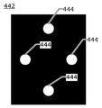
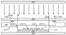
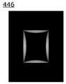
도 4a 내지 도 4i는 실시예에서 사용되는 공간 필터, 방사선 분포, 및 시스템의 예시이다.
도 5a 내지 도 5c는 실시예에서 사용되는 성형가능 재료의 점도, 선량, 강도 및 노광 시간의 예시이다.
도 6은 실시예에서 사용되는 방법의 예시이다.
도면에 걸쳐, 동일한 참조 번호 및 문자는 달리 언급되지 않는 한 도시된 실시예의 유사한 특징, 요소, 성분 또는 부분을 나타내기 위해 사용된다. 또한, 이제 본 개시내용은 도면을 참조하여 상세히 설명되지만, 이는 예시된 예시적인 실시예와 관련하여 이루어진다. 첨부된 청구항에 의해 정의된 본 개시내용의 진정한 범위 및 사상 내에서 설명된 예시적인 실시예에 대해 변경 및 수정이 이루어질 수 있는 것으로 의도된다.
| 유체 | 증점 선량 | 상대 점도 증가 | 점도 범위(mPa·s) |
| #1 | 1.4 - 3.5 mJ/cm2 | 1.1x - 100x | 11 내지 1000 |
| #2 | 1 - 2.5 mJ/cm2 | 1.1x - 100x | 11 내지 1000 |
Claims (15)
- 템플릿으로 성형가능 재료를 임프린팅하도록 구성된 임프린팅 시스템이며, 상기 임프린팅 시스템은,
상기 템플릿을 보유지지하도록 구성되는 템플릿 척과;
기판을 보유지지하도록 구성되는 기판 척과;
템플릿을 상기 기판 상의 상기 성형가능 재료에 접촉시키도록 구성되는 위치결정 시스템과;
- 상기 템플릿은 패터닝 특징부를 포함하는 패턴 영역을 가짐 -;
- 상기 패턴 영역은 상기 패턴 영역을 둘러싸는 경계 에지를 포함함 -;
- 상기 경계 에지는 복수의 코너 및 상기 복수의 코너의 각각을 연결하는 복수의 에지를 포함함 -;
상기 성형가능 재료를 겔화(gelling) 방사선 분포 패턴으로 조명하도록 구성된 조명 시스템
- 상기 조명 시스템은 복수의 개구를 갖고, 상기 복수의 개구 중의 각각의 개구는 겔화 방사선 분포 패턴을 생성하기 위해 사용되는 상기 템플릿의 상기 복수의 코너 중의 2개의 코너로부터 등거리에 위치됨 -;
- 상기 겔화 방사선 분포 패턴은 상기 경계 에지의 복수의 코너의 각각에서의 최소 겔화 선량으로부터 상기 경계 에지의 각각의 중심에서의 피크 겔화 선량까지 변화하는 구배 선량을 갖는 겔화 선량을 가짐 -
을 포함하는 임프린팅 시스템. - 제1항에 있어서, 상기 구배 선량은 상기 경계 에지의 상기 복수의 코너의 각각에서의 상기 최소 겔화 선량으로부터 상기 경계 에지의 각각의 상기 중심에서의 상기 피크 겔화 선량까지 점진적으로 변화하는 임프린팅 시스템.
- 제1항에 있어서, 상기 구배 선량은 상기 경계 에지의 상기 복수의 코너의 각각에서의 상기 최소 겔화 선량으로부터 상기 경계 에지의 각각의 상기 중심에서의 상기 피크 겔화 선량까지 단계적으로 변화하는 임프린팅 시스템.
- 제1항에 있어서, 상기 조명 시스템은 상기 패턴 영역을 경화 방사선 분포 패턴으로 조명하도록 더 구성되는 임프린팅 시스템.
- 제4항에 있어서, 상기 조명 시스템은,
상기 경화 방사선 분포 패턴을 생성하는 화학 에너지 공급원과;
공간 필터로서,
상기 화학 에너지 공급원과 상기 템플릿 사이의 광학 경로 내의 제1 위치; 및
상기 화학 에너지 공급원과 상기 템플릿 사이의 상기 광학 경로 내가 아닌 제2 위치
에 배치되도록 구성되는, 공간 필터를 포함하고;
상기 공간 필터가 상기 제1 위치에 있을 때, 상기 화학 에너지 공급원은 상기 템플릿의 상기 경계 에지에서 상기 겔화 방사선 분포 패턴을 생성하도록 구성되며;
상기 공간 필터가 상기 제2 위치에 있을 때, 상기 화학 에너지 공급원은 상기 패턴 영역 내에 상기 경화 방사선 분포 패턴을 생성하도록 구성되는 임프린팅 시스템. - 제1항에 있어서, 상기 복수의 개구 중의 각각의 개구는 상기 공간 필터가 상기 제1 위치에 있을 때 상기 템플릿의 상기 경계 에지로부터 오프셋되는 임프린팅 시스템.
- 제4항에 있어서, 상기 조명 시스템은,
상기 경화 방사선 분포 패턴을 생성하는 제1 화학 에너지 공급원과;
상기 겔화 방사선 분포 패턴을 생성하는 제2 화학 에너지 공급원을 포함하는 임프린팅 시스템. - 제7항에 있어서, 상기 제2 화학 에너지 공급원은 복수의 에너지 공급원을 포함하고, 상기 복수의 에너지 공급원의 각각은 상기 복수의 개구 중의 하나의 개구와 연관되고, 상기 복수의 에너지 공급원 중의 각각의 에너지 공급원은 상기 복수의 코너 중의 2개의 코너에서의 상기 최소 겔화 선량으로부터 상기 경계 에지 중 하나의 상기 중심에서의 상기 피크 겔화 선량까지 점진적으로 변화하는 상기 구배 선량의 일부를 생성하는 임프린팅 시스템.
- 제7항에 있어서, 상기 제2 화학 에너지 공급원은 복수의 에너지 공급원을 포함하고, 상기 복수의 에너지 공급원의 각각은 상기 복수의 개구 중의 하나의 개구와 연관되고, 상기 복수의 에너지 공급원 중의 각각의 에너지 공급원은 상기 복수의 코너 중의 2개의 코너에서의 상기 최소 겔화 선량으로부터 상기 경계 에지 중 하나의 상기 중심에서의 상기 피크 겔화 선량까지 단계적으로 변화하는 상기 구배 선량의 일부를 생성하는 임프린팅 시스템.
- 패터닝 특징부를 포함하는 패턴 영역을 갖는 템플릿에 의해 기판 상의 성형가능 재료를 임프린팅하도록 구성되는 임프린팅 방법이며, 상기 패턴 영역은 상기 패턴 영역을 둘러싸는 경계 에지를 포함하고, 상기 경계 에지는 복수의 코너 및 상기 복수의 코너의 각각을 연결하는 복수의 에지를 포함하고, 상기 방법은,
상기 템플릿을 상기 기판 상의 상기 성형가능 재료에 접촉시키는 단계와;
겔화 방사선 분포 패턴으로 상기 성형가능 재료를 조명하는 단계로서, 상기 겔화 방사선 분포 패턴은 상기 복수의 코너의 각각에서의 최소 겔화 선량으로부터 상기 경계 에지의 각각의 중심에서의 피크 겔화 선량까지 변화하는 구배 선량을 갖는 겔화 선량을 갖는, 조명 단계와;
- 상기 겔화 방사선 분포 패턴은 복수의 개구로부터 나오고, 상기 복수의 개구 중의 각각의 개구는 겔화 방사선 분포 패턴을 생성하기 위해 사용되는 상기 템플릿의 상기 복수의 코너 중의 2개의 코너로부터 등거리에 위치됨 -
상기 패턴 영역을 경화 방사선 분포 패턴으로 조명하는 단계를 포함하는 임프린팅 방법. - 제10항에 있어서, 상기 구배 선량은 상기 경계 에지의 상기 복수의 코너의 각각에서의 상기 최소 겔화 선량으로부터 상기 경계 에지의 각각의 상기 중심에서의 상기 피크 겔화 선량까지 점진적으로 변화하는 임프린팅 방법.
- 제10항에 있어서, 상기 구배 선량은 상기 경계 에지의 상기 복수의 코너의 각각에서의 상기 최소 겔화 선량으로부터 상기 경계 에지의 각각의 상기 중심에서의 상기 피크 겔화 선량까지 단계적으로 변화하는 임프린팅 방법.
- 제10항에 있어서, 상기 방법은
상기 겔화 방사선 분포 패턴을 생성하기 위해 화학 에너지 공급원과 상기 템플릿 사이의 광학 경로 내의 제1 위치에 공간 필터를 배치하는 단계와;
상기 패턴 영역을 상기 경화 방사선 분포 패턴으로 조명하기 위해 상기 화학 에너지 공급원과 상기 템플릿 사이의 상기 광학 경로 내가 아닌 제2 위치에 상기 공간 필터를 배치하는 단계를 더 포함하는 임프린팅 방법. - 제10항에 있어서,
제1 화학 에너지 공급원이 상기 패턴 영역을 상기 경화 방사선 분포 패턴으로 조명하기 위해 사용되며;
제2 화학 에너지 공급원이 상기 패턴 영역을 상기 경화 방사선 분포 패턴으로 조명하기 위해 사용되는 임프린팅 방법. - 임프린팅 방법에 의해 물품을 제조하는 방법이며, 상기 임프린팅 방법은 패터닝 특징부를 포함하는 패턴 영역을 갖는 템플릿으로 기판 상의 성형가능 재료를 임프린팅하도록 구성되고, 상기 패턴 영역은 상기 패턴 영역을 둘러싸는 경계 에지를 포함하고, 상기 경계 에지는 복수의 코너 및 상기 복수의 코너의 각각을 연결하는 복수의 에지를 포함하고, 상기 물품을 제조하는 방법은,
상기 템플릿을 상기 기판 상의 상기 성형가능 재료에 접촉시키는 단계와;
겔화 방사선 분포 패턴으로 상기 성형가능 재료를 조명하는 단계로서, 상기 겔화 방사선 분포 패턴은 상기 복수의 코너의 각각에서의 최소 겔화 선량으로부터 상기 경계 에지의 각각의 중심에서의 피크 겔화 선량까지 변화하는 구배 선량을 갖는 겔화 선량을 갖는, 조명 단계와;
- 상기 겔화 방사선 분포 패턴은 복수의 개구로부터 나오고, 상기 복수의 개구 중의 각각의 개구는 겔화 방사선 분포 패턴을 생성하기 위해 사용되는 상기 템플릿의 상기 복수의 코너 중의 2개의 코너로부터 등거리에 위치됨 -
상기 패턴 영역을 경화 방사선 분포 패턴으로 조명하는 단계와;
상기 패턴이 형성된 상기 기판을 처리하는 단계로서, 상기 물품은 상기 처리된 기판으로부터 제조되는, 처리 단계를 포함하는 물품을 제조하는 방법.
Applications Claiming Priority (2)
| Application Number | Priority Date | Filing Date | Title |
|---|---|---|---|
| US16/118,794 | 2018-08-31 | ||
| US16/118,794 US10976657B2 (en) | 2018-08-31 | 2018-08-31 | System and method for illuminating edges of an imprint field with a gradient dosage |
Publications (2)
| Publication Number | Publication Date |
|---|---|
| KR20200026063A true KR20200026063A (ko) | 2020-03-10 |
| KR102547578B1 KR102547578B1 (ko) | 2023-06-26 |
Family
ID=69640666
Family Applications (1)
| Application Number | Title | Priority Date | Filing Date |
|---|---|---|---|
| KR1020190102092A Active KR102547578B1 (ko) | 2018-08-31 | 2019-08-21 | 임프린트 필드의 에지를 구배 선량으로 조명하기 위한 시스템 및 방법 |
Country Status (3)
| Country | Link |
|---|---|
| US (1) | US10976657B2 (ko) |
| JP (1) | JP6752343B2 (ko) |
| KR (1) | KR102547578B1 (ko) |
Families Citing this family (4)
| Publication number | Priority date | Publication date | Assignee | Title |
|---|---|---|---|---|
| US10663869B2 (en) * | 2017-12-11 | 2020-05-26 | Canon Kabushiki Kaisha | Imprint system and imprinting process with spatially non-uniform illumination |
| US11181819B2 (en) * | 2019-05-31 | 2021-11-23 | Canon Kabushiki Kaisha | Frame curing method for extrusion control |
| JP7383564B2 (ja) * | 2020-05-27 | 2023-11-20 | キヤノン株式会社 | インプリント方法、インプリント装置、および物品の製造方法 |
| US11747731B2 (en) | 2020-11-20 | 2023-09-05 | Canon Kabishiki Kaisha | Curing a shaped film using multiple images of a spatial light modulator |
Citations (5)
| Publication number | Priority date | Publication date | Assignee | Title |
|---|---|---|---|---|
| JP2013069919A (ja) * | 2011-09-22 | 2013-04-18 | Toshiba Corp | インプリント方法およびインプリント装置 |
| JP2014027016A (ja) * | 2012-07-24 | 2014-02-06 | Canon Inc | インプリント装置、および、物品製造方法 |
| JP2015106670A (ja) * | 2013-12-02 | 2015-06-08 | パナソニックIpマネジメント株式会社 | 微細構造の形成方法、および微細構造の製造装置 |
| KR20170010001A (ko) * | 2014-06-09 | 2017-01-25 | 캐논 가부시끼가이샤 | 임프린트 장치 및 물품의 제조 방법 |
| KR20180062360A (ko) * | 2016-11-30 | 2018-06-08 | 캐논 가부시끼가이샤 | 임프린트 방법, 임프린트 장치, 형, 및 물품 제조 방법 |
Family Cites Families (26)
| Publication number | Priority date | Publication date | Assignee | Title |
|---|---|---|---|---|
| US5168304A (en) * | 1988-08-22 | 1992-12-01 | Nikon Corporation | Exposure apparatus |
| CA2132005A1 (en) * | 1992-04-06 | 1993-10-14 | Jang Fung Chen | Method for improved lithographic patterning in a semiconductor fabrication process |
| JPH0950951A (ja) * | 1995-08-04 | 1997-02-18 | Nikon Corp | リソグラフィ方法およびリソグラフィ装置 |
| US6936194B2 (en) | 2002-09-05 | 2005-08-30 | Molecular Imprints, Inc. | Functional patterning material for imprint lithography processes |
| US20040065252A1 (en) | 2002-10-04 | 2004-04-08 | Sreenivasan Sidlgata V. | Method of forming a layer on a substrate to facilitate fabrication of metrology standards |
| US8349241B2 (en) | 2002-10-04 | 2013-01-08 | Molecular Imprints, Inc. | Method to arrange features on a substrate to replicate features having minimal dimensional variability |
| US6960532B2 (en) * | 2003-02-28 | 2005-11-01 | International Business Machines Corporation | Suppressing lithography at a wafer edge |
| US7157036B2 (en) | 2003-06-17 | 2007-01-02 | Molecular Imprints, Inc | Method to reduce adhesion between a conformable region and a pattern of a mold |
| US8076386B2 (en) | 2004-02-23 | 2011-12-13 | Molecular Imprints, Inc. | Materials for imprint lithography |
| JP4481698B2 (ja) | 2004-03-29 | 2010-06-16 | キヤノン株式会社 | 加工装置 |
| KR20060013245A (ko) * | 2004-08-06 | 2006-02-09 | 삼성전자주식회사 | 조리개를 갖는 웨이퍼 에지 노광기 |
| KR20070086766A (ko) | 2004-12-01 | 2007-08-27 | 몰레큘러 임프린츠 인코퍼레이티드 | 임프린트 리소그래피 공정용 열관리를 위한 노출 방법 |
| US20080303187A1 (en) | 2006-12-29 | 2008-12-11 | Molecular Imprints, Inc. | Imprint Fluid Control |
| US8361371B2 (en) | 2008-02-08 | 2013-01-29 | Molecular Imprints, Inc. | Extrusion reduction in imprint lithography |
| JP4799575B2 (ja) * | 2008-03-06 | 2011-10-26 | 株式会社東芝 | インプリント方法 |
| WO2009153925A1 (ja) | 2008-06-17 | 2009-12-23 | 株式会社ニコン | ナノインプリント方法及び装置 |
| JP5532854B2 (ja) * | 2009-11-25 | 2014-06-25 | 大日本印刷株式会社 | パターン形成方法、パターン形成装置、ナノインプリントモールド及びナノインプリントモールドの製造方法 |
| JP2014120604A (ja) * | 2012-12-17 | 2014-06-30 | Canon Inc | インプリント装置、デバイス製造方法及びインプリント装置に用いられる型 |
| JP6111783B2 (ja) * | 2013-03-27 | 2017-04-12 | 大日本印刷株式会社 | インプリント方法およびインプリント装置 |
| JP2015144193A (ja) * | 2014-01-31 | 2015-08-06 | 株式会社東芝 | インプリント方法、テンプレートおよびインプリント装置 |
| JP6632270B2 (ja) | 2014-09-08 | 2020-01-22 | キヤノン株式会社 | インプリント装置、インプリント方法および物品の製造方法 |
| US10634993B2 (en) | 2016-12-12 | 2020-04-28 | Canon Kabushiki Kaisha | Fluid droplet methodology and apparatus for imprint lithography |
| CN111247623B (zh) * | 2017-10-17 | 2024-03-08 | 佳能株式会社 | 压印装置和物品制造方法 |
| JP6650980B2 (ja) | 2017-10-17 | 2020-02-19 | キヤノン株式会社 | インプリント装置、及び、物品の製造方法 |
| WO2019078060A1 (ja) | 2017-10-17 | 2019-04-25 | キヤノン株式会社 | インプリント装置、及び、物品の製造方法 |
| US10663869B2 (en) * | 2017-12-11 | 2020-05-26 | Canon Kabushiki Kaisha | Imprint system and imprinting process with spatially non-uniform illumination |
-
2018
- 2018-08-31 US US16/118,794 patent/US10976657B2/en active Active
-
2019
- 2019-08-21 KR KR1020190102092A patent/KR102547578B1/ko active Active
- 2019-08-23 JP JP2019153175A patent/JP6752343B2/ja active Active
Patent Citations (5)
| Publication number | Priority date | Publication date | Assignee | Title |
|---|---|---|---|---|
| JP2013069919A (ja) * | 2011-09-22 | 2013-04-18 | Toshiba Corp | インプリント方法およびインプリント装置 |
| JP2014027016A (ja) * | 2012-07-24 | 2014-02-06 | Canon Inc | インプリント装置、および、物品製造方法 |
| JP2015106670A (ja) * | 2013-12-02 | 2015-06-08 | パナソニックIpマネジメント株式会社 | 微細構造の形成方法、および微細構造の製造装置 |
| KR20170010001A (ko) * | 2014-06-09 | 2017-01-25 | 캐논 가부시끼가이샤 | 임프린트 장치 및 물품의 제조 방법 |
| KR20180062360A (ko) * | 2016-11-30 | 2018-06-08 | 캐논 가부시끼가이샤 | 임프린트 방법, 임프린트 장치, 형, 및 물품 제조 방법 |
Also Published As
| Publication number | Publication date |
|---|---|
| JP6752343B2 (ja) | 2020-09-09 |
| US20200073232A1 (en) | 2020-03-05 |
| KR102547578B1 (ko) | 2023-06-26 |
| US10976657B2 (en) | 2021-04-13 |
| JP2020038962A (ja) | 2020-03-12 |
Similar Documents
| Publication | Publication Date | Title |
|---|---|---|
| CN1262883C (zh) | 影印用于平版印刷工艺中的自动化液体分配的方法和系统 | |
| KR102921784B1 (ko) | 압출 제어를 위한 프레임 경화 방법 | |
| KR102547578B1 (ko) | 임프린트 필드의 에지를 구배 선량으로 조명하기 위한 시스템 및 방법 | |
| US12099295B2 (en) | Imprint apparatuses and article manufacturing methods applying viscosity increases without curing of imprint material | |
| KR102698310B1 (ko) | 적하물 패턴을 생성하는 방법, 적하물 패턴에 의해 막을 형성하는 시스템, 및 적하물 패턴에 의해 물품을 제조하는 방법 | |
| KR102196382B1 (ko) | 임프린트 물질의 확산을 제어하기 위한 방법 | |
| KR102780456B1 (ko) | 웨이퍼 프로세스, 장치, 및 물품 제조 방법 | |
| KR20210052256A (ko) | 슈퍼스트레이트 척, 사용 방법 및 물품의 제조 방법 | |
| JP6650980B2 (ja) | インプリント装置、及び、物品の製造方法 | |
| KR102602905B1 (ko) | 성형 장치 및 물품 제조 방법 | |
| TW202105470A (zh) | 壓印裝置及物品的製造方法 | |
| JP2021135504A (ja) | 均一光強度のための露光装置及びその使用方法 | |
| US11281095B2 (en) | Frame curing template and system and method of using the frame curing template | |
| US11373861B2 (en) | System and method of cleaning mesa sidewalls of a template | |
| JP2021068846A (ja) | インプリント装置、インプリント方法及び物品の製造方法 | |
| JP6951483B2 (ja) | 質量速度変動フィーチャを有するテンプレート、テンプレートを使用するナノインプリントリソグラフィ装置、およびテンプレートを使用する方法 | |
| JP2025088749A (ja) | メサ側壁コーティングを有するインプリントテンプレートの使用する方法および製造する方法 | |
| JP2019102606A (ja) | インプリント方法、インプリント装置及び物品の製造方法 | |
| JP2026037894A (ja) | プログラム、情報処理装置、膜形成装置、膜形成方法、および物品製造方法 | |
| KR20230161886A (ko) | 평탄화 공정, 장치 및 물품 제조 방법 |
Legal Events
| Date | Code | Title | Description |
|---|---|---|---|
| PA0109 | Patent application |
St.27 status event code: A-0-1-A10-A12-nap-PA0109 |
|
| PG1501 | Laying open of application |
St.27 status event code: A-1-1-Q10-Q12-nap-PG1501 |
|
| A201 | Request for examination | ||
| PA0201 | Request for examination |
St.27 status event code: A-1-2-D10-D11-exm-PA0201 |
|
| D13-X000 | Search requested |
St.27 status event code: A-1-2-D10-D13-srh-X000 |
|
| D14-X000 | Search report completed |
St.27 status event code: A-1-2-D10-D14-srh-X000 |
|
| E902 | Notification of reason for refusal | ||
| PE0902 | Notice of grounds for rejection |
St.27 status event code: A-1-2-D10-D21-exm-PE0902 |
|
| P11-X000 | Amendment of application requested |
St.27 status event code: A-2-2-P10-P11-nap-X000 |
|
| P13-X000 | Application amended |
St.27 status event code: A-2-2-P10-P13-nap-X000 |
|
| E701 | Decision to grant or registration of patent right | ||
| PE0701 | Decision of registration |
St.27 status event code: A-1-2-D10-D22-exm-PE0701 |
|
| GRNT | Written decision to grant | ||
| PR0701 | Registration of establishment |
St.27 status event code: A-2-4-F10-F11-exm-PR0701 |
|
| PR1002 | Payment of registration fee |
St.27 status event code: A-2-2-U10-U11-oth-PR1002 Fee payment year number: 1 |
|
| PG1601 | Publication of registration |
St.27 status event code: A-4-4-Q10-Q13-nap-PG1601 |
|
| P22-X000 | Classification modified |
St.27 status event code: A-4-4-P10-P22-nap-X000 |