KR20200026672A - 반도체 발광소자를 이용한 백라이트 유닛 - Google Patents
반도체 발광소자를 이용한 백라이트 유닛 Download PDFInfo
- Publication number
- KR20200026672A KR20200026672A KR1020190068833A KR20190068833A KR20200026672A KR 20200026672 A KR20200026672 A KR 20200026672A KR 1020190068833 A KR1020190068833 A KR 1020190068833A KR 20190068833 A KR20190068833 A KR 20190068833A KR 20200026672 A KR20200026672 A KR 20200026672A
- Authority
- KR
- South Korea
- Prior art keywords
- light
- disposed
- light diffusion
- backlight unit
- light emitting
- Prior art date
- Legal status (The legal status is an assumption and is not a legal conclusion. Google has not performed a legal analysis and makes no representation as to the accuracy of the status listed.)
- Granted
Links
Images





Classifications
-
- G—PHYSICS
- G02—OPTICS
- G02F—OPTICAL DEVICES OR ARRANGEMENTS FOR THE CONTROL OF LIGHT BY MODIFICATION OF THE OPTICAL PROPERTIES OF THE MEDIA OF THE ELEMENTS INVOLVED THEREIN; NON-LINEAR OPTICS; FREQUENCY-CHANGING OF LIGHT; OPTICAL LOGIC ELEMENTS; OPTICAL ANALOGUE/DIGITAL CONVERTERS
- G02F1/00—Devices or arrangements for the control of the intensity, colour, phase, polarisation or direction of light arriving from an independent light source, e.g. switching, gating or modulating; Non-linear optics
- G02F1/01—Devices or arrangements for the control of the intensity, colour, phase, polarisation or direction of light arriving from an independent light source, e.g. switching, gating or modulating; Non-linear optics for the control of the intensity, phase, polarisation or colour
- G02F1/13—Devices or arrangements for the control of the intensity, colour, phase, polarisation or direction of light arriving from an independent light source, e.g. switching, gating or modulating; Non-linear optics for the control of the intensity, phase, polarisation or colour based on liquid crystals, e.g. single liquid crystal display cells
- G02F1/133—Constructional arrangements; Operation of liquid crystal cells; Circuit arrangements
- G02F1/1333—Constructional arrangements; Manufacturing methods
- G02F1/1335—Structural association of cells with optical devices, e.g. polarisers or reflectors
- G02F1/1336—Illuminating devices
- G02F1/133602—Direct backlight
- G02F1/133606—Direct backlight including a specially adapted diffusing, scattering or light controlling members
-
- G—PHYSICS
- G02—OPTICS
- G02F—OPTICAL DEVICES OR ARRANGEMENTS FOR THE CONTROL OF LIGHT BY MODIFICATION OF THE OPTICAL PROPERTIES OF THE MEDIA OF THE ELEMENTS INVOLVED THEREIN; NON-LINEAR OPTICS; FREQUENCY-CHANGING OF LIGHT; OPTICAL LOGIC ELEMENTS; OPTICAL ANALOGUE/DIGITAL CONVERTERS
- G02F1/00—Devices or arrangements for the control of the intensity, colour, phase, polarisation or direction of light arriving from an independent light source, e.g. switching, gating or modulating; Non-linear optics
- G02F1/01—Devices or arrangements for the control of the intensity, colour, phase, polarisation or direction of light arriving from an independent light source, e.g. switching, gating or modulating; Non-linear optics for the control of the intensity, phase, polarisation or colour
- G02F1/13—Devices or arrangements for the control of the intensity, colour, phase, polarisation or direction of light arriving from an independent light source, e.g. switching, gating or modulating; Non-linear optics for the control of the intensity, phase, polarisation or colour based on liquid crystals, e.g. single liquid crystal display cells
- G02F1/133—Constructional arrangements; Operation of liquid crystal cells; Circuit arrangements
- G02F1/1333—Constructional arrangements; Manufacturing methods
- G02F1/1335—Structural association of cells with optical devices, e.g. polarisers or reflectors
- G02F1/1336—Illuminating devices
- G02F1/133602—Direct backlight
- G02F1/133603—Direct backlight with LEDs
-
- G—PHYSICS
- G02—OPTICS
- G02F—OPTICAL DEVICES OR ARRANGEMENTS FOR THE CONTROL OF LIGHT BY MODIFICATION OF THE OPTICAL PROPERTIES OF THE MEDIA OF THE ELEMENTS INVOLVED THEREIN; NON-LINEAR OPTICS; FREQUENCY-CHANGING OF LIGHT; OPTICAL LOGIC ELEMENTS; OPTICAL ANALOGUE/DIGITAL CONVERTERS
- G02F1/00—Devices or arrangements for the control of the intensity, colour, phase, polarisation or direction of light arriving from an independent light source, e.g. switching, gating or modulating; Non-linear optics
- G02F1/01—Devices or arrangements for the control of the intensity, colour, phase, polarisation or direction of light arriving from an independent light source, e.g. switching, gating or modulating; Non-linear optics for the control of the intensity, phase, polarisation or colour
- G02F1/13—Devices or arrangements for the control of the intensity, colour, phase, polarisation or direction of light arriving from an independent light source, e.g. switching, gating or modulating; Non-linear optics for the control of the intensity, phase, polarisation or colour based on liquid crystals, e.g. single liquid crystal display cells
- G02F1/133—Constructional arrangements; Operation of liquid crystal cells; Circuit arrangements
- G02F1/1333—Constructional arrangements; Manufacturing methods
- G02F1/1335—Structural association of cells with optical devices, e.g. polarisers or reflectors
- G02F1/1336—Illuminating devices
- G02F1/133602—Direct backlight
- G02F1/133608—Direct backlight including particular frames or supporting means
-
- G—PHYSICS
- G02—OPTICS
- G02F—OPTICAL DEVICES OR ARRANGEMENTS FOR THE CONTROL OF LIGHT BY MODIFICATION OF THE OPTICAL PROPERTIES OF THE MEDIA OF THE ELEMENTS INVOLVED THEREIN; NON-LINEAR OPTICS; FREQUENCY-CHANGING OF LIGHT; OPTICAL LOGIC ELEMENTS; OPTICAL ANALOGUE/DIGITAL CONVERTERS
- G02F1/00—Devices or arrangements for the control of the intensity, colour, phase, polarisation or direction of light arriving from an independent light source, e.g. switching, gating or modulating; Non-linear optics
- G02F1/01—Devices or arrangements for the control of the intensity, colour, phase, polarisation or direction of light arriving from an independent light source, e.g. switching, gating or modulating; Non-linear optics for the control of the intensity, phase, polarisation or colour
- G02F1/13—Devices or arrangements for the control of the intensity, colour, phase, polarisation or direction of light arriving from an independent light source, e.g. switching, gating or modulating; Non-linear optics for the control of the intensity, phase, polarisation or colour based on liquid crystals, e.g. single liquid crystal display cells
- G02F1/133—Constructional arrangements; Operation of liquid crystal cells; Circuit arrangements
- G02F1/1333—Constructional arrangements; Manufacturing methods
- G02F1/1335—Structural association of cells with optical devices, e.g. polarisers or reflectors
- G02F1/1336—Illuminating devices
- G02F1/133602—Direct backlight
- G02F1/133611—Direct backlight including means for improving the brightness uniformity
-
- H—ELECTRICITY
- H10—SEMICONDUCTOR DEVICES; ELECTRIC SOLID-STATE DEVICES NOT OTHERWISE PROVIDED FOR
- H10H—INORGANIC LIGHT-EMITTING SEMICONDUCTOR DEVICES HAVING POTENTIAL BARRIERS
- H10H20/00—Individual inorganic light-emitting semiconductor devices having potential barriers, e.g. light-emitting diodes [LED]
- H10H20/01—Manufacture or treatment
-
- H—ELECTRICITY
- H10—SEMICONDUCTOR DEVICES; ELECTRIC SOLID-STATE DEVICES NOT OTHERWISE PROVIDED FOR
- H10H—INORGANIC LIGHT-EMITTING SEMICONDUCTOR DEVICES HAVING POTENTIAL BARRIERS
- H10H20/00—Individual inorganic light-emitting semiconductor devices having potential barriers, e.g. light-emitting diodes [LED]
- H10H20/80—Constructional details
- H10H20/85—Packages
- H10H20/851—Wavelength conversion means
- H10H20/8511—Wavelength conversion means characterised by their material, e.g. binder
- H10H20/8512—Wavelength conversion materials
-
- H—ELECTRICITY
- H10—SEMICONDUCTOR DEVICES; ELECTRIC SOLID-STATE DEVICES NOT OTHERWISE PROVIDED FOR
- H10H—INORGANIC LIGHT-EMITTING SEMICONDUCTOR DEVICES HAVING POTENTIAL BARRIERS
- H10H20/00—Individual inorganic light-emitting semiconductor devices having potential barriers, e.g. light-emitting diodes [LED]
- H10H20/80—Constructional details
- H10H20/85—Packages
- H10H20/855—Optical field-shaping means, e.g. lenses
-
- H—ELECTRICITY
- H10—SEMICONDUCTOR DEVICES; ELECTRIC SOLID-STATE DEVICES NOT OTHERWISE PROVIDED FOR
- H10W—GENERIC PACKAGES, INTERCONNECTIONS, CONNECTORS OR OTHER CONSTRUCTIONAL DETAILS OF DEVICES COVERED BY CLASS H10
- H10W90/00—Package configurations
-
- G—PHYSICS
- G02—OPTICS
- G02F—OPTICAL DEVICES OR ARRANGEMENTS FOR THE CONTROL OF LIGHT BY MODIFICATION OF THE OPTICAL PROPERTIES OF THE MEDIA OF THE ELEMENTS INVOLVED THEREIN; NON-LINEAR OPTICS; FREQUENCY-CHANGING OF LIGHT; OPTICAL LOGIC ELEMENTS; OPTICAL ANALOGUE/DIGITAL CONVERTERS
- G02F1/00—Devices or arrangements for the control of the intensity, colour, phase, polarisation or direction of light arriving from an independent light source, e.g. switching, gating or modulating; Non-linear optics
- G02F1/01—Devices or arrangements for the control of the intensity, colour, phase, polarisation or direction of light arriving from an independent light source, e.g. switching, gating or modulating; Non-linear optics for the control of the intensity, phase, polarisation or colour
- G02F1/13—Devices or arrangements for the control of the intensity, colour, phase, polarisation or direction of light arriving from an independent light source, e.g. switching, gating or modulating; Non-linear optics for the control of the intensity, phase, polarisation or colour based on liquid crystals, e.g. single liquid crystal display cells
- G02F1/133—Constructional arrangements; Operation of liquid crystal cells; Circuit arrangements
- G02F1/1333—Constructional arrangements; Manufacturing methods
- G02F1/1335—Structural association of cells with optical devices, e.g. polarisers or reflectors
- G02F1/1336—Illuminating devices
- G02F1/133614—Illuminating devices using photoluminescence, e.g. phosphors illuminated by UV or blue light
-
- G—PHYSICS
- G02—OPTICS
- G02F—OPTICAL DEVICES OR ARRANGEMENTS FOR THE CONTROL OF LIGHT BY MODIFICATION OF THE OPTICAL PROPERTIES OF THE MEDIA OF THE ELEMENTS INVOLVED THEREIN; NON-LINEAR OPTICS; FREQUENCY-CHANGING OF LIGHT; OPTICAL LOGIC ELEMENTS; OPTICAL ANALOGUE/DIGITAL CONVERTERS
- G02F1/00—Devices or arrangements for the control of the intensity, colour, phase, polarisation or direction of light arriving from an independent light source, e.g. switching, gating or modulating; Non-linear optics
- G02F1/01—Devices or arrangements for the control of the intensity, colour, phase, polarisation or direction of light arriving from an independent light source, e.g. switching, gating or modulating; Non-linear optics for the control of the intensity, phase, polarisation or colour
- G02F1/13—Devices or arrangements for the control of the intensity, colour, phase, polarisation or direction of light arriving from an independent light source, e.g. switching, gating or modulating; Non-linear optics for the control of the intensity, phase, polarisation or colour based on liquid crystals, e.g. single liquid crystal display cells
- G02F1/133—Constructional arrangements; Operation of liquid crystal cells; Circuit arrangements
- G02F1/1333—Constructional arrangements; Manufacturing methods
- G02F1/1335—Structural association of cells with optical devices, e.g. polarisers or reflectors
- G02F1/1336—Illuminating devices
- G02F1/133615—Edge-illuminating devices, i.e. illuminating from the side
-
- H—ELECTRICITY
- H10—SEMICONDUCTOR DEVICES; ELECTRIC SOLID-STATE DEVICES NOT OTHERWISE PROVIDED FOR
- H10H—INORGANIC LIGHT-EMITTING SEMICONDUCTOR DEVICES HAVING POTENTIAL BARRIERS
- H10H20/00—Individual inorganic light-emitting semiconductor devices having potential barriers, e.g. light-emitting diodes [LED]
- H10H20/01—Manufacture or treatment
- H10H20/036—Manufacture or treatment of packages
- H10H20/0361—Manufacture or treatment of packages of wavelength conversion means
-
- H—ELECTRICITY
- H10—SEMICONDUCTOR DEVICES; ELECTRIC SOLID-STATE DEVICES NOT OTHERWISE PROVIDED FOR
- H10H—INORGANIC LIGHT-EMITTING SEMICONDUCTOR DEVICES HAVING POTENTIAL BARRIERS
- H10H20/00—Individual inorganic light-emitting semiconductor devices having potential barriers, e.g. light-emitting diodes [LED]
- H10H20/80—Constructional details
- H10H20/85—Packages
- H10H20/855—Optical field-shaping means, e.g. lenses
- H10H20/856—Reflecting means
Landscapes
- Physics & Mathematics (AREA)
- Nonlinear Science (AREA)
- Mathematical Physics (AREA)
- Chemical & Material Sciences (AREA)
- Crystallography & Structural Chemistry (AREA)
- General Physics & Mathematics (AREA)
- Optics & Photonics (AREA)
- Planar Illumination Modules (AREA)
Abstract
Description
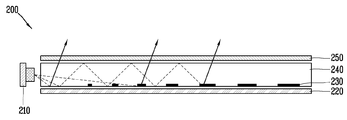
도 2는 에지 방식의 백라이트 유닛을 나타내는 단면도이다.
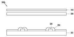
도 3 및 4는 직하 방식의 백라이트 유닛을 나타내는 단면도이다.
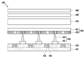
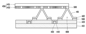
도 5은 본 발명에 따른 백라이트 유닛의 단면을 나타내는 개념도이다.
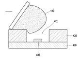
도 6 및 7은 본 발명에 따른 백라이트 유닛의 제조 방법을 나타내는 개념도이다.
도 8 내지 11은 본 발명에 따른 백라이트 유닛에 포함된 스페이서의 구조를 나타내는 개념도이다.
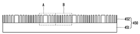
도 12는 광확산층의 단면도이다.
도 13은 광학산패턴을 나타내는 개념도이다.
Claims (10)
- 베이스 기판;
상기 베이스 기판 상에 배치되고, 복수의 홈을 구비하는 격벽;
상기 베이스 기판 상에 조립되고, 상기 홈 내부에 배치되는 반도체 발광소자;
상기 반도체 발광소자를 덮도록 상기 홈 내부에 형성되고, 소정 파장대의 빛을 흡수하여 상기 소정 파장대의 빛과 다른 파장대의 빛을 발광하는 형광체층;
상기 형광체층 상측에 배치되며, 빛을 확산시키는 광확산층; 및
상기 격벽과 상기 광확산층 사이에 배치되는 스페이서를 포함하고,
상기 스페이서는,
상기 격벽에 부착되는 바디부; 및
상기 광확산층과 상기 형광체층이 서로 이격되도록, 상기 광확산층을 향하는 방향으로 돌출되어, 상기 광확산층에 부착되는 돌출부를 구비하는 것을 특징으로 하는 백라이트 유닛. - 제1항에 있어서,
상기 스페이서는 필름형태로 이루어지고,
상기 돌출부는 상기 바디부의 일부가 벤딩되어 형성되는 것을 특징으로 하는 백라이트 유닛. - 제2항에 있어서,
상기 격벽과 상기 돌출부는 서로 이격되는 것을 특징으로 하는 백라이트 유닛. - 제1항에 있어서,
상기 바디부는,
상기 격벽의 양면 중 상기 광확산층을 향하는 일면 상에 부착되는 것을 특징으로 하는 백라이트 유닛. - 제4항에 있어서,
상기 바디부는,
상기 격벽의 전체 영역 중 홈이 형성된 영역을 제외한 나머지 영역에 배치되는 것을 특징으로 하는 백라이트 유닛. - 제1항에 있어서,
상기 바디부와 상기 격벽 사이, 상기 돌출부와 상기 광확산층 사이에 각각 배치되는 접착층을 더 포함하는 것을 특징으로 하는 백라이트 유닛. - 제1항에 있어서,
상기 광확산층은,
베이스필름; 및
상기 베이스필름 상에 형성되며, 산란 입자를 포함하는 광확산패턴으로 이루어지는 것을 특징으로 하는 백라이트 유닛. - 제7항에 있어서,
상기 광확산패턴에 포함된 산란 입자의 단위 면적 당 질량은,
상기 반도체 발광소자와 인접할수록 증가하는 것을 특징으로 하는 백라이트 유닛. - 제8항에 있어서,
상기 돌출부는,
상기 광확산패턴에 포함된 산란 입자의 단위 면적 당 질량이 가장 적은 영역과 오버랩되도록 배치되는 것을 특징으로 하는 백라이트 유닛. - 제9항에 있어서,
상기 광확산패턴은,
상기 베이스필름의 양면 중 상기 격벽을 향하는 일면 상에 배치되는 것을 특징으로 하는 백라이트 유닛.
Priority Applications (3)
| Application Number | Priority Date | Filing Date | Title |
|---|---|---|---|
| KR1020190068833A KR102721663B1 (ko) | 2019-06-11 | 2019-06-11 | 반도체 발광소자를 이용한 백라이트 유닛 |
| US17/618,170 US12032239B2 (en) | 2019-06-11 | 2020-02-06 | Backlight unit using semiconductor light-emitting element |
| PCT/KR2020/001694 WO2020251131A1 (ko) | 2019-06-11 | 2020-02-06 | 반도체 발광소자를 이용한 백라이트 유닛 |
Applications Claiming Priority (1)
| Application Number | Priority Date | Filing Date | Title |
|---|---|---|---|
| KR1020190068833A KR102721663B1 (ko) | 2019-06-11 | 2019-06-11 | 반도체 발광소자를 이용한 백라이트 유닛 |
Publications (2)
| Publication Number | Publication Date |
|---|---|
| KR20200026672A true KR20200026672A (ko) | 2020-03-11 |
| KR102721663B1 KR102721663B1 (ko) | 2024-10-25 |
Family
ID=69809772
Family Applications (1)
| Application Number | Title | Priority Date | Filing Date |
|---|---|---|---|
| KR1020190068833A Active KR102721663B1 (ko) | 2019-06-11 | 2019-06-11 | 반도체 발광소자를 이용한 백라이트 유닛 |
Country Status (3)
| Country | Link |
|---|---|
| US (1) | US12032239B2 (ko) |
| KR (1) | KR102721663B1 (ko) |
| WO (1) | WO2020251131A1 (ko) |
Cited By (1)
| Publication number | Priority date | Publication date | Assignee | Title |
|---|---|---|---|---|
| WO2024006266A1 (en) * | 2022-06-30 | 2024-01-04 | Lumileds Llc | Led array with air-spaced optics |
Families Citing this family (2)
| Publication number | Priority date | Publication date | Assignee | Title |
|---|---|---|---|---|
| CN115047674B (zh) * | 2022-06-14 | 2023-04-25 | 惠科股份有限公司 | 背光模组及显示装置 |
| TWI866554B (zh) * | 2023-10-20 | 2024-12-11 | 瑞軒科技股份有限公司 | 背光模組 |
Citations (3)
| Publication number | Priority date | Publication date | Assignee | Title |
|---|---|---|---|---|
| US20170139276A1 (en) * | 2014-10-31 | 2017-05-18 | eLux Inc. | Emissive Display with Printed Light Modification Structures |
| KR20170061535A (ko) * | 2015-11-26 | 2017-06-05 | 엘지디스플레이 주식회사 | 백라이트 유닛 및 이를 이용한 액정 표시 장치 |
| US20180080625A1 (en) * | 2016-09-16 | 2018-03-22 | Nichia Corporation | Light emitting device |
Family Cites Families (20)
| Publication number | Priority date | Publication date | Assignee | Title |
|---|---|---|---|---|
| WO2004068182A2 (en) * | 2003-01-24 | 2004-08-12 | Digital Optics International Corporation | High density illumination system |
| JP4491634B2 (ja) | 2004-01-23 | 2010-06-30 | 日本電気株式会社 | 直下型バックライト及び表示装置 |
| TWI283321B (en) * | 2004-06-18 | 2007-07-01 | Au Optronics Corp | Supporter and LED light-source module using the same |
| JP4543813B2 (ja) * | 2004-08-04 | 2010-09-15 | ソニー株式会社 | バックライト装置及びこのバックライト装置を備えた液晶表示装置 |
| CN100437282C (zh) * | 2005-10-21 | 2008-11-26 | 鸿富锦精密工业(深圳)有限公司 | 背光模组和其灯管夹持装置 |
| JP2008270144A (ja) * | 2007-03-22 | 2008-11-06 | Furukawa Electric Co Ltd:The | ライトボックス |
| TWI368792B (en) * | 2007-11-09 | 2012-07-21 | Au Optronics Corp | Lcd device, backlight module, thereof, with partition wall and method for manufacturing the same |
| JP5540610B2 (ja) * | 2009-09-03 | 2014-07-02 | 株式会社Jvcケンウッド | 光量制御部材、面光源装置及び表示装置 |
| JP5631776B2 (ja) * | 2010-03-03 | 2014-11-26 | 株式会社東芝 | 照明装置およびこれを備えた液晶表示装置 |
| WO2012023458A1 (ja) * | 2010-08-19 | 2012-02-23 | シャープ株式会社 | 照明装置、表示装置及びテレビ受信装置 |
| WO2012029002A1 (en) * | 2010-08-31 | 2012-03-08 | Koninklijke Philips Electronics N.V. | Led-based lighting units with substantially sealed leds |
| JP2012174634A (ja) * | 2011-02-24 | 2012-09-10 | Sharp Corp | 光源モジュールおよび光学部材 |
| KR102034067B1 (ko) | 2012-08-10 | 2019-11-08 | 엘지이노텍 주식회사 | 조명유닛 |
| KR102252237B1 (ko) | 2014-12-22 | 2021-05-14 | 엘지전자 주식회사 | 백라이트 유닛 및 이를 포함하는 표시장치 |
| WO2017002307A1 (ja) * | 2015-07-01 | 2017-01-05 | パナソニックIpマネジメント株式会社 | バックライト装置および液晶表示装置 |
| US10061159B2 (en) * | 2015-08-11 | 2018-08-28 | Canon Kabushiki Kaisha | Light-emitting apparatus and image display apparatus with a partition member separating adjacent light source units |
| TWI564623B (zh) * | 2015-10-08 | 2017-01-01 | 友達光電股份有限公司 | 顯示裝置及其組裝方法 |
| EP3273297B1 (en) * | 2016-07-20 | 2021-05-26 | Nichia Corporation | Light emitting device |
| JP7048888B2 (ja) * | 2018-04-06 | 2022-04-06 | 日亜化学工業株式会社 | 光源装置の製造方法 |
| CN110970408B (zh) * | 2018-09-28 | 2024-07-19 | 日亚化学工业株式会社 | 发光装置 |
-
2019
- 2019-06-11 KR KR1020190068833A patent/KR102721663B1/ko active Active
-
2020
- 2020-02-06 WO PCT/KR2020/001694 patent/WO2020251131A1/ko not_active Ceased
- 2020-02-06 US US17/618,170 patent/US12032239B2/en active Active
Patent Citations (3)
| Publication number | Priority date | Publication date | Assignee | Title |
|---|---|---|---|---|
| US20170139276A1 (en) * | 2014-10-31 | 2017-05-18 | eLux Inc. | Emissive Display with Printed Light Modification Structures |
| KR20170061535A (ko) * | 2015-11-26 | 2017-06-05 | 엘지디스플레이 주식회사 | 백라이트 유닛 및 이를 이용한 액정 표시 장치 |
| US20180080625A1 (en) * | 2016-09-16 | 2018-03-22 | Nichia Corporation | Light emitting device |
Cited By (1)
| Publication number | Priority date | Publication date | Assignee | Title |
|---|---|---|---|---|
| WO2024006266A1 (en) * | 2022-06-30 | 2024-01-04 | Lumileds Llc | Led array with air-spaced optics |
Also Published As
| Publication number | Publication date |
|---|---|
| KR102721663B1 (ko) | 2024-10-25 |
| US20220326570A1 (en) | 2022-10-13 |
| WO2020251131A1 (ko) | 2020-12-17 |
| US12032239B2 (en) | 2024-07-09 |
Similar Documents
| Publication | Publication Date | Title |
|---|---|---|
| US12493214B2 (en) | Planar lighting device | |
| CN206557505U (zh) | 光源组件、显示装置及电子设备 | |
| JP4498286B2 (ja) | 面状光源装置およびこの面状光源装置を用いた表示装置 | |
| CN114442371A (zh) | 显示背板及显示装置 | |
| CN104023427B (zh) | 照明装置 | |
| US12032239B2 (en) | Backlight unit using semiconductor light-emitting element | |
| EP2530375B1 (en) | Light guide design for edge-illumination in a backlight unit | |
| US20100118509A1 (en) | Light source package, liquid crystal display device including light source package, and method of manufacturing the same | |
| CN115826294B (zh) | 背光模组、显示模组以及显示装置 | |
| WO2013114977A1 (ja) | 線状光源装置、面発光装置、および液晶表示装置 | |
| CN106950749A (zh) | 背光单元和显示装置 | |
| US20210026056A1 (en) | Lamp using semiconductor light-emitting devices | |
| JP4594859B2 (ja) | 照明装置及びこれを用いた画像表示装置 | |
| CN110112277B (zh) | 一种发光二极管、背光模组及显示装置 | |
| KR20120114520A (ko) | 발광 소자 및 이를 이용한 백 라이트 유닛과 액정 표시 장치 | |
| KR20200026656A (ko) | 반도체 발광 소자를 이용한 램프 | |
| KR20130013971A (ko) | 백라이트 유닛 | |
| KR20120045445A (ko) | 면발광장치 및 액정표시장치 |
Legal Events
| Date | Code | Title | Description |
|---|---|---|---|
| PA0109 | Patent application |
Patent event code: PA01091R01D Comment text: Patent Application Patent event date: 20190611 |
|
| G15R | Request for early publication | ||
| PG1501 | Laying open of application |
Comment text: Request for Early Opening Patent event code: PG15011R01I Patent event date: 20200221 |
|
| A201 | Request for examination | ||
| PA0201 | Request for examination |
Patent event code: PA02012R01D Patent event date: 20220613 Comment text: Request for Examination of Application Patent event code: PA02011R01I Patent event date: 20190611 Comment text: Patent Application |
|
| E902 | Notification of reason for refusal | ||
| PE0902 | Notice of grounds for rejection |
Comment text: Notification of reason for refusal Patent event date: 20230817 Patent event code: PE09021S01D |
|
| E90F | Notification of reason for final refusal | ||
| PE0902 | Notice of grounds for rejection |
Comment text: Final Notice of Reason for Refusal Patent event date: 20240228 Patent event code: PE09021S02D |
|
| E701 | Decision to grant or registration of patent right | ||
| PE0701 | Decision of registration |
Patent event code: PE07011S01D Comment text: Decision to Grant Registration Patent event date: 20240730 |
|
| GRNT | Written decision to grant | ||
| PR0701 | Registration of establishment |
Comment text: Registration of Establishment Patent event date: 20241021 Patent event code: PR07011E01D |
|
| PR1002 | Payment of registration fee |
Payment date: 20241022 End annual number: 3 Start annual number: 1 |
|
| PG1601 | Publication of registration |