KR20200027046A - 차폐 메모리 아키텍처를 위한 장치 및 방법 - Google Patents
차폐 메모리 아키텍처를 위한 장치 및 방법 Download PDFInfo
- Publication number
- KR20200027046A KR20200027046A KR1020207006113A KR20207006113A KR20200027046A KR 20200027046 A KR20200027046 A KR 20200027046A KR 1020207006113 A KR1020207006113 A KR 1020207006113A KR 20207006113 A KR20207006113 A KR 20207006113A KR 20200027046 A KR20200027046 A KR 20200027046A
- Authority
- KR
- South Korea
- Prior art keywords
- memory cell
- line
- memory
- plate
- digit line
- Prior art date
- Legal status (The legal status is an assumption and is not a legal conclusion. Google has not performed a legal analysis and makes no representation as to the accuracy of the status listed.)
- Granted
Links
Images








Classifications
-
- G—PHYSICS
- G11—INFORMATION STORAGE
- G11C—STATIC STORES
- G11C5/00—Details of stores covered by group G11C11/00
- G11C5/06—Arrangements for interconnecting storage elements electrically, e.g. by wiring
- G11C5/063—Voltage and signal distribution in integrated semi-conductor memory access lines, e.g. word-line, bit-line, cross-over resistance, propagation delay
-
- H—ELECTRICITY
- H10—SEMICONDUCTOR DEVICES; ELECTRIC SOLID-STATE DEVICES NOT OTHERWISE PROVIDED FOR
- H10W—GENERIC PACKAGES, INTERCONNECTIONS, CONNECTORS OR OTHER CONSTRUCTIONAL DETAILS OF DEVICES COVERED BY CLASS H10
- H10W42/00—Arrangements for protection of devices
- H10W42/20—Arrangements for protection of devices protecting against electromagnetic or particle radiation, e.g. light, X-rays, gamma-rays or electrons
-
- G—PHYSICS
- G11—INFORMATION STORAGE
- G11C—STATIC STORES
- G11C11/00—Digital stores characterised by the use of particular electric or magnetic storage elements; Storage elements therefor
- G11C11/02—Digital stores characterised by the use of particular electric or magnetic storage elements; Storage elements therefor using magnetic elements
- G11C11/16—Digital stores characterised by the use of particular electric or magnetic storage elements; Storage elements therefor using magnetic elements using elements in which the storage effect is based on magnetic spin effect
- G11C11/165—Auxiliary circuits
- G11C11/1653—Address circuits or decoders
-
- G—PHYSICS
- G11—INFORMATION STORAGE
- G11C—STATIC STORES
- G11C11/00—Digital stores characterised by the use of particular electric or magnetic storage elements; Storage elements therefor
- G11C11/02—Digital stores characterised by the use of particular electric or magnetic storage elements; Storage elements therefor using magnetic elements
- G11C11/16—Digital stores characterised by the use of particular electric or magnetic storage elements; Storage elements therefor using magnetic elements using elements in which the storage effect is based on magnetic spin effect
- G11C11/165—Auxiliary circuits
- G11C11/1659—Cell access
-
- G—PHYSICS
- G11—INFORMATION STORAGE
- G11C—STATIC STORES
- G11C11/00—Digital stores characterised by the use of particular electric or magnetic storage elements; Storage elements therefor
- G11C11/21—Digital stores characterised by the use of particular electric or magnetic storage elements; Storage elements therefor using electric elements
- G11C11/22—Digital stores characterised by the use of particular electric or magnetic storage elements; Storage elements therefor using electric elements using ferroelectric elements
- G11C11/221—Digital stores characterised by the use of particular electric or magnetic storage elements; Storage elements therefor using electric elements using ferroelectric elements using ferroelectric capacitors
-
- G—PHYSICS
- G11—INFORMATION STORAGE
- G11C—STATIC STORES
- G11C11/00—Digital stores characterised by the use of particular electric or magnetic storage elements; Storage elements therefor
- G11C11/21—Digital stores characterised by the use of particular electric or magnetic storage elements; Storage elements therefor using electric elements
- G11C11/22—Digital stores characterised by the use of particular electric or magnetic storage elements; Storage elements therefor using electric elements using ferroelectric elements
- G11C11/225—Auxiliary circuits
- G11C11/2253—Address circuits or decoders
-
- G—PHYSICS
- G11—INFORMATION STORAGE
- G11C—STATIC STORES
- G11C11/00—Digital stores characterised by the use of particular electric or magnetic storage elements; Storage elements therefor
- G11C11/21—Digital stores characterised by the use of particular electric or magnetic storage elements; Storage elements therefor using electric elements
- G11C11/22—Digital stores characterised by the use of particular electric or magnetic storage elements; Storage elements therefor using electric elements using ferroelectric elements
- G11C11/225—Auxiliary circuits
- G11C11/2253—Address circuits or decoders
- G11C11/2255—Bit-line or column circuits
-
- G—PHYSICS
- G11—INFORMATION STORAGE
- G11C—STATIC STORES
- G11C11/00—Digital stores characterised by the use of particular electric or magnetic storage elements; Storage elements therefor
- G11C11/21—Digital stores characterised by the use of particular electric or magnetic storage elements; Storage elements therefor using electric elements
- G11C11/22—Digital stores characterised by the use of particular electric or magnetic storage elements; Storage elements therefor using electric elements using ferroelectric elements
- G11C11/225—Auxiliary circuits
- G11C11/2253—Address circuits or decoders
- G11C11/2257—Word-line or row circuits
-
- G—PHYSICS
- G11—INFORMATION STORAGE
- G11C—STATIC STORES
- G11C11/00—Digital stores characterised by the use of particular electric or magnetic storage elements; Storage elements therefor
- G11C11/21—Digital stores characterised by the use of particular electric or magnetic storage elements; Storage elements therefor using electric elements
- G11C11/22—Digital stores characterised by the use of particular electric or magnetic storage elements; Storage elements therefor using electric elements using ferroelectric elements
- G11C11/225—Auxiliary circuits
- G11C11/2259—Cell access
-
- G—PHYSICS
- G11—INFORMATION STORAGE
- G11C—STATIC STORES
- G11C11/00—Digital stores characterised by the use of particular electric or magnetic storage elements; Storage elements therefor
- G11C11/21—Digital stores characterised by the use of particular electric or magnetic storage elements; Storage elements therefor using electric elements
- G11C11/22—Digital stores characterised by the use of particular electric or magnetic storage elements; Storage elements therefor using electric elements using ferroelectric elements
- G11C11/225—Auxiliary circuits
- G11C11/2273—Reading or sensing circuits or methods
-
- G—PHYSICS
- G11—INFORMATION STORAGE
- G11C—STATIC STORES
- G11C11/00—Digital stores characterised by the use of particular electric or magnetic storage elements; Storage elements therefor
- G11C11/21—Digital stores characterised by the use of particular electric or magnetic storage elements; Storage elements therefor using electric elements
- G11C11/22—Digital stores characterised by the use of particular electric or magnetic storage elements; Storage elements therefor using electric elements using ferroelectric elements
- G11C11/225—Auxiliary circuits
- G11C11/2275—Writing or programming circuits or methods
-
- G—PHYSICS
- G11—INFORMATION STORAGE
- G11C—STATIC STORES
- G11C11/00—Digital stores characterised by the use of particular electric or magnetic storage elements; Storage elements therefor
- G11C11/21—Digital stores characterised by the use of particular electric or magnetic storage elements; Storage elements therefor using electric elements
- G11C11/34—Digital stores characterised by the use of particular electric or magnetic storage elements; Storage elements therefor using electric elements using semiconductor devices
- G11C11/40—Digital stores characterised by the use of particular electric or magnetic storage elements; Storage elements therefor using electric elements using semiconductor devices using transistors
- G11C11/401—Digital stores characterised by the use of particular electric or magnetic storage elements; Storage elements therefor using electric elements using semiconductor devices using transistors forming cells needing refreshing or charge regeneration, i.e. dynamic cells
- G11C11/4063—Auxiliary circuits, e.g. for addressing, decoding, driving, writing, sensing or timing
- G11C11/407—Auxiliary circuits, e.g. for addressing, decoding, driving, writing, sensing or timing for memory cells of the field-effect type
- G11C11/408—Address circuits
-
- G—PHYSICS
- G11—INFORMATION STORAGE
- G11C—STATIC STORES
- G11C11/00—Digital stores characterised by the use of particular electric or magnetic storage elements; Storage elements therefor
- G11C11/21—Digital stores characterised by the use of particular electric or magnetic storage elements; Storage elements therefor using electric elements
- G11C11/34—Digital stores characterised by the use of particular electric or magnetic storage elements; Storage elements therefor using electric elements using semiconductor devices
- G11C11/40—Digital stores characterised by the use of particular electric or magnetic storage elements; Storage elements therefor using electric elements using semiconductor devices using transistors
- G11C11/401—Digital stores characterised by the use of particular electric or magnetic storage elements; Storage elements therefor using electric elements using semiconductor devices using transistors forming cells needing refreshing or charge regeneration, i.e. dynamic cells
- G11C11/4063—Auxiliary circuits, e.g. for addressing, decoding, driving, writing, sensing or timing
- G11C11/407—Auxiliary circuits, e.g. for addressing, decoding, driving, writing, sensing or timing for memory cells of the field-effect type
- G11C11/408—Address circuits
- G11C11/4085—Word line control circuits, e.g. word line drivers, - boosters, - pull-up, - pull-down, - precharge
-
- G—PHYSICS
- G11—INFORMATION STORAGE
- G11C—STATIC STORES
- G11C11/00—Digital stores characterised by the use of particular electric or magnetic storage elements; Storage elements therefor
- G11C11/21—Digital stores characterised by the use of particular electric or magnetic storage elements; Storage elements therefor using electric elements
- G11C11/34—Digital stores characterised by the use of particular electric or magnetic storage elements; Storage elements therefor using electric elements using semiconductor devices
- G11C11/40—Digital stores characterised by the use of particular electric or magnetic storage elements; Storage elements therefor using electric elements using semiconductor devices using transistors
- G11C11/401—Digital stores characterised by the use of particular electric or magnetic storage elements; Storage elements therefor using electric elements using semiconductor devices using transistors forming cells needing refreshing or charge regeneration, i.e. dynamic cells
- G11C11/4063—Auxiliary circuits, e.g. for addressing, decoding, driving, writing, sensing or timing
- G11C11/407—Auxiliary circuits, e.g. for addressing, decoding, driving, writing, sensing or timing for memory cells of the field-effect type
- G11C11/409—Read-write [R-W] circuits
-
- G—PHYSICS
- G11—INFORMATION STORAGE
- G11C—STATIC STORES
- G11C11/00—Digital stores characterised by the use of particular electric or magnetic storage elements; Storage elements therefor
- G11C11/21—Digital stores characterised by the use of particular electric or magnetic storage elements; Storage elements therefor using electric elements
- G11C11/34—Digital stores characterised by the use of particular electric or magnetic storage elements; Storage elements therefor using electric elements using semiconductor devices
- G11C11/40—Digital stores characterised by the use of particular electric or magnetic storage elements; Storage elements therefor using electric elements using semiconductor devices using transistors
- G11C11/401—Digital stores characterised by the use of particular electric or magnetic storage elements; Storage elements therefor using electric elements using semiconductor devices using transistors forming cells needing refreshing or charge regeneration, i.e. dynamic cells
- G11C11/4063—Auxiliary circuits, e.g. for addressing, decoding, driving, writing, sensing or timing
- G11C11/407—Auxiliary circuits, e.g. for addressing, decoding, driving, writing, sensing or timing for memory cells of the field-effect type
- G11C11/409—Read-write [R-W] circuits
- G11C11/4091—Sense or sense/refresh amplifiers, or associated sense circuitry, e.g. for coupled bit-line precharging, equalising or isolating
-
- G—PHYSICS
- G11—INFORMATION STORAGE
- G11C—STATIC STORES
- G11C11/00—Digital stores characterised by the use of particular electric or magnetic storage elements; Storage elements therefor
- G11C11/21—Digital stores characterised by the use of particular electric or magnetic storage elements; Storage elements therefor using electric elements
- G11C11/34—Digital stores characterised by the use of particular electric or magnetic storage elements; Storage elements therefor using electric elements using semiconductor devices
- G11C11/40—Digital stores characterised by the use of particular electric or magnetic storage elements; Storage elements therefor using electric elements using semiconductor devices using transistors
- G11C11/401—Digital stores characterised by the use of particular electric or magnetic storage elements; Storage elements therefor using electric elements using semiconductor devices using transistors forming cells needing refreshing or charge regeneration, i.e. dynamic cells
- G11C11/4063—Auxiliary circuits, e.g. for addressing, decoding, driving, writing, sensing or timing
- G11C11/407—Auxiliary circuits, e.g. for addressing, decoding, driving, writing, sensing or timing for memory cells of the field-effect type
- G11C11/409—Read-write [R-W] circuits
- G11C11/4094—Bit-line management or control circuits
-
- G—PHYSICS
- G11—INFORMATION STORAGE
- G11C—STATIC STORES
- G11C13/00—Digital stores characterised by the use of storage elements not covered by groups G11C11/00, G11C23/00, or G11C25/00
- G11C13/0002—Digital stores characterised by the use of storage elements not covered by groups G11C11/00, G11C23/00, or G11C25/00 using resistive RAM [RRAM] elements
- G11C13/0021—Auxiliary circuits
- G11C13/0023—Address circuits or decoders
-
- G—PHYSICS
- G11—INFORMATION STORAGE
- G11C—STATIC STORES
- G11C13/00—Digital stores characterised by the use of storage elements not covered by groups G11C11/00, G11C23/00, or G11C25/00
- G11C13/0002—Digital stores characterised by the use of storage elements not covered by groups G11C11/00, G11C23/00, or G11C25/00 using resistive RAM [RRAM] elements
- G11C13/0021—Auxiliary circuits
- G11C13/003—Cell access
-
- G—PHYSICS
- G11—INFORMATION STORAGE
- G11C—STATIC STORES
- G11C5/00—Details of stores covered by group G11C11/00
- G11C5/02—Disposition of storage elements, e.g. in the form of a matrix array
- G11C5/025—Geometric lay-out considerations of storage- and peripheral-blocks in a semiconductor storage device
-
- G—PHYSICS
- G11—INFORMATION STORAGE
- G11C—STATIC STORES
- G11C7/00—Arrangements for writing information into, or reading information out from, a digital store
- G11C7/02—Arrangements for writing information into, or reading information out from, a digital store with means for avoiding parasitic signals
-
- G—PHYSICS
- G11—INFORMATION STORAGE
- G11C—STATIC STORES
- G11C7/00—Arrangements for writing information into, or reading information out from, a digital store
- G11C7/18—Bit line organisation; Bit line lay-out
-
- H—ELECTRICITY
- H10—SEMICONDUCTOR DEVICES; ELECTRIC SOLID-STATE DEVICES NOT OTHERWISE PROVIDED FOR
- H10B—ELECTRONIC MEMORY DEVICES
- H10B12/00—Dynamic random access memory [DRAM] devices
- H10B12/30—DRAM devices comprising one-transistor - one-capacitor [1T-1C] memory cells
- H10B12/48—Data lines or contacts therefor
- H10B12/482—Bit lines
-
- H—ELECTRICITY
- H10—SEMICONDUCTOR DEVICES; ELECTRIC SOLID-STATE DEVICES NOT OTHERWISE PROVIDED FOR
- H10B—ELECTRONIC MEMORY DEVICES
- H10B53/00—Ferroelectric RAM [FeRAM] devices comprising ferroelectric memory capacitors
- H10B53/30—Ferroelectric RAM [FeRAM] devices comprising ferroelectric memory capacitors characterised by the memory core region
-
- H—ELECTRICITY
- H10—SEMICONDUCTOR DEVICES; ELECTRIC SOLID-STATE DEVICES NOT OTHERWISE PROVIDED FOR
- H10W—GENERIC PACKAGES, INTERCONNECTIONS, CONNECTORS OR OTHER CONSTRUCTIONAL DETAILS OF DEVICES COVERED BY CLASS H10
- H10W20/00—Interconnections in chips, wafers or substrates
- H10W20/40—Interconnections external to wafers or substrates, e.g. back-end-of-line [BEOL] metallisations or vias connecting to gate electrodes
- H10W20/41—Interconnections external to wafers or substrates, e.g. back-end-of-line [BEOL] metallisations or vias connecting to gate electrodes characterised by their conductive parts
- H10W20/43—Layouts of interconnections
-
- G—PHYSICS
- G11—INFORMATION STORAGE
- G11C—STATIC STORES
- G11C2213/00—Indexing scheme relating to G11C13/00 for features not covered by this group
- G11C2213/70—Resistive array aspects
- G11C2213/82—Array having, for accessing a cell, a word line, a bit line and a plate or source line receiving different potentials
-
- G—PHYSICS
- G11—INFORMATION STORAGE
- G11C—STATIC STORES
- G11C7/00—Arrangements for writing information into, or reading information out from, a digital store
- G11C7/06—Sense amplifiers; Associated circuits, e.g. timing or triggering circuits
- G11C7/08—Control thereof
-
- G—PHYSICS
- G11—INFORMATION STORAGE
- G11C—STATIC STORES
- G11C7/00—Arrangements for writing information into, or reading information out from, a digital store
- G11C7/10—Input/output [I/O] data interface arrangements, e.g. I/O data control circuits, I/O data buffers
- G11C7/1051—Data output circuits, e.g. read-out amplifiers, data output buffers, data output registers, data output level conversion circuits
-
- G—PHYSICS
- G11—INFORMATION STORAGE
- G11C—STATIC STORES
- G11C7/00—Arrangements for writing information into, or reading information out from, a digital store
- G11C7/10—Input/output [I/O] data interface arrangements, e.g. I/O data control circuits, I/O data buffers
- G11C7/1078—Data input circuits, e.g. write amplifiers, data input buffers, data input registers, data input level conversion circuits
- G11C7/1096—Write circuits, e.g. I/O line write drivers
-
- H—ELECTRICITY
- H10—SEMICONDUCTOR DEVICES; ELECTRIC SOLID-STATE DEVICES NOT OTHERWISE PROVIDED FOR
- H10B—ELECTRONIC MEMORY DEVICES
- H10B12/00—Dynamic random access memory [DRAM] devices
- H10B12/30—DRAM devices comprising one-transistor - one-capacitor [1T-1C] memory cells
-
- H—ELECTRICITY
- H10—SEMICONDUCTOR DEVICES; ELECTRIC SOLID-STATE DEVICES NOT OTHERWISE PROVIDED FOR
- H10B—ELECTRONIC MEMORY DEVICES
- H10B53/00—Ferroelectric RAM [FeRAM] devices comprising ferroelectric memory capacitors
- H10B53/20—Ferroelectric RAM [FeRAM] devices comprising ferroelectric memory capacitors characterised by the three-dimensional [3D] arrangements, e.g. with cells on different height levels
Landscapes
- Engineering & Computer Science (AREA)
- Computer Hardware Design (AREA)
- Microelectronics & Electronic Packaging (AREA)
- Power Engineering (AREA)
- Physics & Mathematics (AREA)
- Semiconductor Memories (AREA)
- Dram (AREA)
- Geometry (AREA)
- Health & Medical Sciences (AREA)
- Electromagnetism (AREA)
- Toxicology (AREA)
Abstract
Description
도 2a는 본 개시내용의 실시형태에 따른, 메모리 셀의 열을 포함하는 예시적인 회로의 개략도.
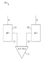
도 2b는 본 개시내용의 실시형태에 따른, 감지 컴포넌트의 개략도.
도 3은 본 개시내용의 실시형태에 따른, 메모리 셀의 단일의 행을 포함하는 예시적인 회로에 대한 일반적인 회로 구성의 개략도.
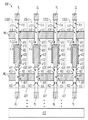
도 4a 및 도 4b는 도 3의 일반적인 회로 구성의 더 구체적인 회로 구현예의 도면.
도 4c 및 도 4d는 본 개시내용의 실시형태에 따른, 메모리 셀을 나타내는 메모리 어레이의 일부의 단면측 뷰를 도시하는 도면.
도 5는 본 개시내용의 실시형태에 따른, 메모리 셀의 2개의 행의 적층된 구성을 포함하는 예시적인 회로에 대한 일반적인 회로 구성의 개략도.
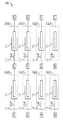
도 6a 내지 도 6c는 도 5의 일반적인 회로 구성의 더 구체적인 회로 구현예의 도면.
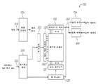
도 7은 본 개시내용의 실시형태에 따른, 메모리의 블록도.
도 8은 본 개시내용의 실시형태에 따른, 셀의 2개의 행의 적층된 구성을 포함하는 예시적인 회로에 대한 일반적인 회로 구성의 개략도.
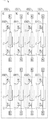
도 9a 내지 도 9c는 도 8의 일반적인 회로 구성의 더 구체적인 회로 구현예의 도면.
도 10은 본 개시내용의 다양한 실시형태에 따른, 메모리를 지원하는 메모리 어레이를 포함하는 메모리의 일부의 블록도.
도 11은 본 개시내용의 다양한 실시형태에 따른, 강유전성 메모리를 지원하는 시스템을 도시하는 도면.
Claims (20)
- 장치로서,
플레이트 라인에 연결된 제1 단부 및 디지트 라인에 연결된 제2 단부를 가진 저장 컴포넌트를 포함하는 제1 메모리 셀; 및
디지트 라인에 연결된 제1 단부 및 플레이트 라인에 연결된 제2 단부를 가진 저장 컴포넌트를 포함하는 제2 메모리 셀을 포함하되,
상기 제2 메모리 셀의 상기 디지트 라인은 상기 제1 메모리 셀의 상기 플레이트 라인과 인접한, 장치. - 제1항에 있어서, 상기 제1 메모리 셀의 상기 디지트 라인은 상기 제2 메모리 셀의 상기 플레이트 라인과 인접한, 장치.
- 제1항에 있어서,
플레이트 라인에 연결된 제1 단부 및 디지트 라인에 연결된 제2 단부를 가진 저장 컴포넌트를 포함하는 제3 메모리 셀을 더 포함하되,
상기 제2 메모리 셀의 상기 디지트 라인은 상기 제3 메모리 셀의 상기 플레이트 라인과 인접한, 장치. - 제3항에 있어서,
메모리 셀의 제1 층; 및
상기 제1 메모리 셀, 상기 제2 메모리 셀, 및 상기 제3 메모리 셀을 포함하는 메모리 셀의 제2 층을 더 포함하는, 장치. - 제4항에 있어서,
상기 메모리 셀의 제1 층에 포함된 제4 메모리 셀을 더 포함하되, 상기 제4 메모리 셀은 플레이트 라인에 연결된 제1 단부 및 디지트 라인에 연결된 제2 단부를 가진 저장 컴포넌트를 포함하고,
상기 제4 메모리 셀의 상기 디지트 라인과 상기 제2 메모리 셀의 상기 디지트 라인은 공유된 디지트 라인으로 결합되는, 장치. - 제4항에 있어서,
상기 메모리 셀의 제1 층에 포함된 제4 메모리 셀을 더 포함하되, 상기 제4 메모리 셀은 디지트 라인에 연결된 제1 단부 및 플레이트 라인에 연결된 제2 단부를 가진 저장 컴포넌트를 포함하고,
상기 제2 메모리 셀의 상기 디지트 라인은 상기 제4 메모리 셀의 상기 플레이트 라인과 인접한, 장치. - 제1항에 있어서, 상기 제1 메모리 셀의 상기 제1 저장 컴포넌트의 상기 제1 단부는 제1 선택 컴포넌트를 통해 상기 플레이트 라인에 연결되는, 장치.
- 제7항에 있어서, 상기 제1 메모리 셀의 상기 제1 저장 컴포넌트의 상기 제2 단부는 제2 선택 컴포넌트를 통해 상기 디지트 라인에 연결되는, 장치.
- 제1항에 있어서, 상기 제1 저장 컴포넌트와 상기 제2 저장 컴포넌트는 유전성 커패시터인, 장치.
- 제1항에 있어서, 상기 제1 저장 컴포넌트와 상기 제2 저장 컴포넌트는 강유전성 커패시터인, 장치.
- 장치로서,
메모리 셀의 제1 층;
상기 메모리 셀의 제1 층의 아래에 있는 메모리 셀의 제2 층;
상기 메모리 셀의 제1 층에 포함된 제1 메모리 셀로서, 플레이트 라인에 연결된 제1 단부 및 디지트 라인에 연결된 제2 단부를 가진 저장 컴포넌트를 포함하는, 상기 제1 메모리 셀; 및
상기 메모리 셀의 제2 층에 포함된 제2 메모리 셀로서, 디지트 라인에 연결된 제1 단부 및 플레이트 라인에 연결된 제2 단부를 가진 저장 컴포넌트를 포함하는, 상기 제2 메모리 셀을 포함하되,
상기 제1 메모리 셀의 상기 디지트 라인과 상기 제2 메모리 셀의 상기 디지트 라인은 공유된 디지트 라인으로 결합되는, 장치. - 제11항에 있어서,
상기 메모리 셀의 제1 층에 포함된 제3 메모리 셀로서, 디지트 라인에 연결된 제1 단부 및 플레이트 라인에 연결된 제2 단부를 가진 저장 컴포넌트를 포함하는, 상기 제3 메모리 셀; 및
상기 메모리 셀의 제2 층에 포함된 제4 메모리 셀로서, 플레이트 라인에 연결된 제1 단부 및 디지트 라인에 연결된 제2 단부를 가진 저장 컴포넌트를 포함하는, 상기 제4 메모리 셀을 포함하되,
상기 제3 메모리 셀의 상기 플레이트 라인과 상기 제4 메모리 셀의 상기 플레이트 라인은 공유된 플레이트 라인으로 결합되고; 그리고
상기 제1 메모리 셀과 상기 제2 메모리 셀의 상기 공유된 디지트 라인은 상기 제3 플레이트 라인과 상기 제4 플레이트 라인의 상기 공유된 플레이트 라인과 인접한, 장치. - 제12항에 있어서,
상기 메모리 셀의 제1 층에 포함된 제5 메모리 셀로서, 디지트 라인에 연결된 제1 단부 및 플레이트 라인에 연결된 제2 단부를 가진 저장 컴포넌트를 포함하는, 상기 제5 메모리 셀; 및
상기 메모리 셀의 제2 층에 포함된 제6 메모리 셀로서, 플레이트 라인에 연결된 제1 단부 및 디지트 라인에 연결된 제2 단부를 가진 저장 컴포넌트를 포함하는, 상기 제6 메모리 셀을 포함하되,
상기 제5 메모리 셀의 상기 플레이트 라인과 상기 제6 메모리 셀의 상기 플레이트 라인은 공유된 플레이트 라인으로 결합되고; 그리고
상기 제1 메모리 셀과 상기 제2 메모리 셀의 상기 공유된 디지트 라인은 상기 제5 플레이트 라인과 상기 제6 플레이트 라인의 상기 공유된 플레이트 라인과 인접한, 장치. - 제11항에 있어서,
상기 제1 메모리 셀의 상기 저장 컴포넌트의 제2 단부는 제1 선택 컴포넌트를 통해 상기 디지트 라인에 연결되고; 그리고
상기 제2 메모리 셀의 상기 저장 컴포넌트의 제2 단부는 제2 선택 컴포넌트를 통해 상기 플레이트 라인에 연결되는, 장치. - 제14항에 있어서,
상기 제1 메모리 셀의 상기 저장 컴포넌트의 제1 단부는 제3 선택 컴포넌트를 통해 상기 플레이트 라인에 연결되고; 그리고
상기 제2 메모리 셀의 상기 저장 컴포넌트의 제1 단부는 제4 선택 컴포넌트를 통해 상기 디지트 라인에 연결되는, 장치. - 장치로서,
제1 메모리 층;
상기 제1 메모리 층의 아래에 있는 제2 메모리 층;
상기 제1 메모리 층 내 제1 저장 컴포넌트 및 상기 제2 메모리 층 내 제2 저장 컴포넌트를 포함하는 메모리 셀을 포함하되,
상기 제1 저장 컴포넌트는 플레이트 라인에 연결된 제1 단부 및 디지트 라인에 연결된 제2 단부를 포함하고;
상기 제2 저장 컴포넌트는 플레이트 라인에 연결된 제1 단부 및 디지트 라인에 연결된 제2 단부를 포함하고; 그리고
상기 제1 저장 컴포넌트의 상기 디지트 라인은 상기 제2 저장 컴포넌트의 상기 플레이트 라인과 인접한, 장치. - 제16항에 있어서, 상기 메모리 셀은 제1 메모리 셀이고, 상기 장치는,
상기 제1 메모리 층 내 제1 저장 컴포넌트 및 상기 제2 메모리 층 내 제2 저장 컴포넌트를 포함하는 제2 메모리 셀을 더 포함하되,
상기 제2 메모리 셀의 상기 제1 저장 컴포넌트는 디지트 라인에 연결된 제1 단부 및 플레이트 라인에 연결된 제2 단부를 포함하고;
상기 제2 메모리 셀의 상기 제2 저장 컴포넌트는 디지트 라인에 연결된 제1 단부 및 플레이트 라인에 연결된 제2 단부를 포함하고; 그리고
상기 제1 메모리 셀의 상기 제1 저장 컴포넌트의 상기 디지트 라인은 상기 제2 메모리 셀의 상기 제1 저장 컴포넌트의 상기 플레이트 라인과 인접한, 장치. - 제17항에 있어서,
상기 제1 메모리 층 내 제1 저장 컴포넌트 및 상기 제2 메모리 층 내 제2 저장 컴포넌트를 포함하는 제3 메모리 셀을 더 포함하되,
상기 제3 메모리 셀의 상기 제1 저장 컴포넌트는 디지트 라인에 연결된 제1 단부 및 플레이트 라인에 연결된 제2 단부를 포함하고;
상기 제3 메모리 셀의 상기 제2 저장 컴포넌트는 디지트 라인에 연결된 제1 단부 및 플레이트 라인에 연결된 제2 단부를 포함하고; 그리고
상기 제1 메모리 셀의 상기 제1 저장 컴포넌트의 상기 디지트 라인은 상기 제3 메모리 셀의 상기 제1 저장 컴포넌트의 상기 플레이트 라인과 인접한, 장치. - 제16항에 있어서,
상기 제1 저장 컴포넌트의 제2 단부는 제1 선택 컴포넌트를 통해 상기 디지트 라인에 연결되고; 그리고
상기 제2 저장 컴포넌트의 제2 단부는 제2 선택 컴포넌트를 통해 상기 디지트 라인에 연결되는, 장치. - 제19항에 있어서,
상기 제2 저장 컴포넌트의 제1 단부는 제3 선택 컴포넌트를 통해 상기 플레이트 라인에 연결되고; 그리고
상기 제2 저장 컴포넌트의 제1 단부는 제4 선택 컴포넌트를 통해 상기 플레이트 라인에 연결되는, 장치.
Applications Claiming Priority (3)
| Application Number | Priority Date | Filing Date | Title |
|---|---|---|---|
| US15/691,055 | 2017-08-30 | ||
| US15/691,055 US10446502B2 (en) | 2017-08-30 | 2017-08-30 | Apparatuses and methods for shielded memory architecture |
| PCT/US2018/047377 WO2019046051A1 (en) | 2017-08-30 | 2018-08-21 | APPARATUSES AND METHODS FOR PROTECTED MEMORY ARCHITECTURE |
Publications (2)
| Publication Number | Publication Date |
|---|---|
| KR20200027046A true KR20200027046A (ko) | 2020-03-11 |
| KR102282786B1 KR102282786B1 (ko) | 2021-07-30 |
Family
ID=65435922
Family Applications (1)
| Application Number | Title | Priority Date | Filing Date |
|---|---|---|---|
| KR1020207006113A Active KR102282786B1 (ko) | 2017-08-30 | 2018-08-21 | 차폐 메모리 아키텍처를 위한 장치 및 방법 |
Country Status (7)
| Country | Link |
|---|---|
| US (2) | US10446502B2 (ko) |
| EP (1) | EP3676834A4 (ko) |
| JP (1) | JP6980902B2 (ko) |
| KR (1) | KR102282786B1 (ko) |
| CN (1) | CN111052237A (ko) |
| SG (1) | SG11202000869SA (ko) |
| WO (1) | WO2019046051A1 (ko) |
Cited By (1)
| Publication number | Priority date | Publication date | Assignee | Title |
|---|---|---|---|---|
| KR20220153632A (ko) * | 2020-03-26 | 2022-11-18 | 마이크론 테크놀로지, 인크 | 다중화된 선택 라인을 갖는 메모리 어레이 |
Families Citing this family (22)
| Publication number | Priority date | Publication date | Assignee | Title |
|---|---|---|---|---|
| CN110574160B (zh) | 2017-05-08 | 2023-05-19 | 美光科技公司 | 存储器阵列 |
| CN109087674A (zh) * | 2017-06-14 | 2018-12-25 | 萨摩亚商费洛储存科技股份有限公司 | 铁电内存及其数据读取、写入与制造方法和电容结构 |
| US11043499B2 (en) | 2017-07-27 | 2021-06-22 | Micron Technology, Inc. | Memory arrays comprising memory cells |
| US10446502B2 (en) | 2017-08-30 | 2019-10-15 | Micron, Technology, Inc. | Apparatuses and methods for shielded memory architecture |
| US10868132B2 (en) * | 2017-09-18 | 2020-12-15 | Taiwan Semiconductor Manufacturing Co., Ltd. | Semiconductor device including standard cells with header/footer switch including negative capacitance |
| US10991411B2 (en) | 2018-08-17 | 2021-04-27 | Micron Technology, Inc. | Method and apparatuses for performing a voltage adjustment operation on a section of memory cells based on a quantity of access operations |
| US10431281B1 (en) * | 2018-08-17 | 2019-10-01 | Micron Technology, Inc. | Access schemes for section-based data protection in a memory device |
| US11145358B2 (en) * | 2018-08-31 | 2021-10-12 | Micron Technology, Inc. | Offsetting capacitance of a digit line coupled to storage memory cells coupled to a sense amplifier using offset memory cells |
| US10950618B2 (en) * | 2018-11-29 | 2021-03-16 | Micron Technology, Inc. | Memory arrays |
| US11062763B2 (en) * | 2019-04-09 | 2021-07-13 | Micron Technology, Inc. | Memory array with multiplexed digit lines |
| US10943624B1 (en) * | 2019-08-15 | 2021-03-09 | Micron Technology, Inc. | Countering digit line coupling in memory arrays |
| US11069385B1 (en) * | 2020-03-31 | 2021-07-20 | Micron Technology, Inc. | Integrated assemblies comprising folded-digit-line-configurations |
| US11393832B2 (en) | 2020-07-15 | 2022-07-19 | Ferroelectric Memory Gmbh | Memory cell arrangement |
| US11101291B2 (en) * | 2020-07-15 | 2021-08-24 | Ferroelectric Memory Gmbh | Memory cell arrangement and methods thereof |
| US11309034B2 (en) * | 2020-07-15 | 2022-04-19 | Ferroelectric Memory Gmbh | Memory cell arrangement and methods thereof |
| US11152056B1 (en) * | 2020-09-14 | 2021-10-19 | Micron Technology, Inc. | Integrated assemblies |
| US11170849B1 (en) * | 2020-09-17 | 2021-11-09 | Nxp Usa, Inc. | Memory with select line voltage control |
| US11393822B1 (en) | 2021-05-21 | 2022-07-19 | Micron Technology, Inc. | Thin film transistor deck selection in a memory device |
| JP7457140B2 (ja) * | 2021-07-16 | 2024-03-27 | チャンシン メモリー テクノロジーズ インコーポレイテッド | 半導体構造及びその製造方法 |
| US12550334B2 (en) * | 2021-12-06 | 2026-02-10 | Intel Corporation | Memory with one access transistor for multiple hysteretic capacitors |
| US12125523B2 (en) * | 2022-01-27 | 2024-10-22 | Taiwan Semiconductor Manufacturing Company, Ltd. | Memory device and method of manufacturing the same |
| US20240407151A1 (en) * | 2023-05-30 | 2024-12-05 | Macronix International Co., Ltd. | Memory cell circuit, memory cell array structure and manufacturing method thereof |
Citations (6)
| Publication number | Priority date | Publication date | Assignee | Title |
|---|---|---|---|---|
| KR20010026311A (ko) * | 1999-09-04 | 2001-04-06 | 한신혁 | 강유전체 메모리 |
| JP2003046066A (ja) * | 2001-07-31 | 2003-02-14 | Sony Corp | 強誘電体型不揮発性半導体メモリ、及び、半導体装置 |
| US20040047219A1 (en) * | 2001-11-05 | 2004-03-11 | Yasuyuki Ito | Ferroelectric nonvolatile semiconductor memory |
| US20050047191A1 (en) * | 2003-07-14 | 2005-03-03 | Seiko Epson Corporation | Memory cell and semiconductor memory device |
| US20050122763A1 (en) * | 2003-10-31 | 2005-06-09 | Mitsuhiro Yamamura | Ferroelectric memory device and electronic apparatus |
| KR20090015180A (ko) * | 2006-12-27 | 2009-02-11 | 주식회사 하이닉스반도체 | 강유전체 소자를 적용한 반도체 메모리 장치 및 그 리프레쉬 방법 |
Family Cites Families (35)
| Publication number | Priority date | Publication date | Assignee | Title |
|---|---|---|---|---|
| JPH02148763A (ja) * | 1988-11-29 | 1990-06-07 | Nec Kyushu Ltd | 半導体記憶装置 |
| KR100348577B1 (ko) * | 1999-09-30 | 2002-08-13 | 동부전자 주식회사 | 강유전체 메모리 |
| JP3918515B2 (ja) * | 2001-11-05 | 2007-05-23 | ソニー株式会社 | 強誘電体型不揮発性半導体メモリ |
| JP3756873B2 (ja) * | 2002-11-11 | 2006-03-15 | 沖電気工業株式会社 | 半導体記憶装置 |
| JP3597185B2 (ja) | 2002-11-12 | 2004-12-02 | 沖電気工業株式会社 | 強誘電体メモリ |
| US20040119105A1 (en) * | 2002-12-18 | 2004-06-24 | Wilson Dennis Robert | Ferroelectric memory |
| JP3592321B2 (ja) * | 2003-01-31 | 2004-11-24 | 沖電気工業株式会社 | 強誘電体メモリおよびその判定方法 |
| JP3945498B2 (ja) * | 2003-07-14 | 2007-07-18 | セイコーエプソン株式会社 | メモリセル及び半導体記憶装置 |
| JP2007013011A (ja) * | 2005-07-01 | 2007-01-18 | Seiko Epson Corp | 強誘電体メモリ装置及び表示用駆動ic |
| JP4697668B2 (ja) * | 2006-02-22 | 2011-06-08 | セイコーエプソン株式会社 | 強誘電体メモリ装置、表示用駆動ic及び電子機器 |
| JP4458285B2 (ja) | 2005-12-06 | 2010-04-28 | セイコーエプソン株式会社 | 強誘電体記憶装置 |
| JP2010118128A (ja) | 2008-11-14 | 2010-05-27 | Toshiba Corp | 強誘電体メモリ |
| US8148780B2 (en) * | 2009-03-24 | 2012-04-03 | Micron Technology, Inc. | Devices and systems relating to a memory cell having a floating body |
| US9001577B2 (en) * | 2012-06-01 | 2015-04-07 | Micron Technology, Inc. | Memory cell sensing |
| US9019785B2 (en) * | 2013-09-19 | 2015-04-28 | Micron Technology, Inc. | Data shifting via a number of isolation devices |
| US9786347B1 (en) * | 2016-03-16 | 2017-10-10 | Micron Technology, Inc. | Cell-specific reference generation and sensing |
| US9792973B2 (en) * | 2016-03-18 | 2017-10-17 | Micron Technology, Inc. | Ferroelectric memory cell sensing |
| US9786348B1 (en) * | 2016-04-11 | 2017-10-10 | Micron Technology, Inc. | Dynamic adjustment of memory cell digit line capacitance |
| US9721638B1 (en) * | 2016-05-10 | 2017-08-01 | Micron Technology, Inc. | Boosting a digit line voltage for a write operation |
| US9881661B2 (en) * | 2016-06-03 | 2018-01-30 | Micron Technology, Inc. | Charge mirror-based sensing for ferroelectric memory |
| US9697913B1 (en) * | 2016-06-10 | 2017-07-04 | Micron Technology, Inc. | Ferroelectric memory cell recovery |
| US9892776B2 (en) * | 2016-06-13 | 2018-02-13 | Micron Technology, Inc. | Half density ferroelectric memory and operation |
| US9941021B2 (en) * | 2016-06-16 | 2018-04-10 | Micron Technology, Inc. | Plate defect mitigation techniques |
| US9721639B1 (en) * | 2016-06-21 | 2017-08-01 | Micron Technology, Inc. | Memory cell imprint avoidance |
| US9715919B1 (en) * | 2016-06-21 | 2017-07-25 | Micron Technology, Inc. | Array data bit inversion |
| US9899073B2 (en) * | 2016-06-27 | 2018-02-20 | Micron Technology, Inc. | Multi-level storage in ferroelectric memory |
| US9786349B1 (en) * | 2016-07-01 | 2017-10-10 | Micron Technology, Inc. | Cell performance recovery using cycling techniques |
| US10566040B2 (en) * | 2016-07-29 | 2020-02-18 | Micron Technology, Inc. | Variable page size architecture |
| US10049713B2 (en) * | 2016-08-24 | 2018-08-14 | Micron Technology, Inc. | Full bias sensing in a memory array |
| SG11201901210UA (en) * | 2016-08-31 | 2019-03-28 | Micron Technology Inc | Ferroelectric memory cells |
| US10282108B2 (en) * | 2016-08-31 | 2019-05-07 | Micron Technology, Inc. | Hybrid memory device using different types of capacitors |
| US9779796B1 (en) * | 2016-09-07 | 2017-10-03 | Micron Technology, Inc. | Redundancy array column decoder for memory |
| US10372566B2 (en) * | 2016-09-16 | 2019-08-06 | Micron Technology, Inc. | Storing memory array operational information in nonvolatile subarrays |
| US9886991B1 (en) * | 2016-09-30 | 2018-02-06 | Micron Technology, Inc. | Techniques for sensing logic values stored in memory cells using sense amplifiers that are selectively isolated from digit lines |
| US10446502B2 (en) | 2017-08-30 | 2019-10-15 | Micron, Technology, Inc. | Apparatuses and methods for shielded memory architecture |
-
2017
- 2017-08-30 US US15/691,055 patent/US10446502B2/en active Active
-
2018
- 2018-08-21 EP EP18850121.7A patent/EP3676834A4/en not_active Withdrawn
- 2018-08-21 CN CN201880056038.7A patent/CN111052237A/zh not_active Withdrawn
- 2018-08-21 WO PCT/US2018/047377 patent/WO2019046051A1/en not_active Ceased
- 2018-08-21 JP JP2020511781A patent/JP6980902B2/ja active Active
- 2018-08-21 KR KR1020207006113A patent/KR102282786B1/ko active Active
- 2018-08-21 SG SG11202000869SA patent/SG11202000869SA/en unknown
-
2019
- 2019-09-06 US US16/563,691 patent/US11335644B2/en active Active
Patent Citations (6)
| Publication number | Priority date | Publication date | Assignee | Title |
|---|---|---|---|---|
| KR20010026311A (ko) * | 1999-09-04 | 2001-04-06 | 한신혁 | 강유전체 메모리 |
| JP2003046066A (ja) * | 2001-07-31 | 2003-02-14 | Sony Corp | 強誘電体型不揮発性半導体メモリ、及び、半導体装置 |
| US20040047219A1 (en) * | 2001-11-05 | 2004-03-11 | Yasuyuki Ito | Ferroelectric nonvolatile semiconductor memory |
| US20050047191A1 (en) * | 2003-07-14 | 2005-03-03 | Seiko Epson Corporation | Memory cell and semiconductor memory device |
| US20050122763A1 (en) * | 2003-10-31 | 2005-06-09 | Mitsuhiro Yamamura | Ferroelectric memory device and electronic apparatus |
| KR20090015180A (ko) * | 2006-12-27 | 2009-02-11 | 주식회사 하이닉스반도체 | 강유전체 소자를 적용한 반도체 메모리 장치 및 그 리프레쉬 방법 |
Cited By (2)
| Publication number | Priority date | Publication date | Assignee | Title |
|---|---|---|---|---|
| KR20220153632A (ko) * | 2020-03-26 | 2022-11-18 | 마이크론 테크놀로지, 인크 | 다중화된 선택 라인을 갖는 메모리 어레이 |
| CN115605956A (zh) * | 2020-03-26 | 2023-01-13 | 美光科技公司(Us) | 具有多路复用选择线的存储器阵列 |
Also Published As
| Publication number | Publication date |
|---|---|
| EP3676834A4 (en) | 2021-05-05 |
| KR102282786B1 (ko) | 2021-07-30 |
| US11335644B2 (en) | 2022-05-17 |
| US20190067206A1 (en) | 2019-02-28 |
| JP6980902B2 (ja) | 2021-12-15 |
| US20190393167A1 (en) | 2019-12-26 |
| CN111052237A (zh) | 2020-04-21 |
| JP2020532862A (ja) | 2020-11-12 |
| WO2019046051A1 (en) | 2019-03-07 |
| EP3676834A1 (en) | 2020-07-08 |
| US10446502B2 (en) | 2019-10-15 |
| SG11202000869SA (en) | 2020-03-30 |
Similar Documents
| Publication | Publication Date | Title |
|---|---|---|
| KR102282786B1 (ko) | 차폐 메모리 아키텍처를 위한 장치 및 방법 | |
| JP6964750B2 (ja) | 強誘電体メモリセル及び誘電体メモリセルを含むメモリのための装置及び方法 | |
| KR102369776B1 (ko) | 강유전 메모리 셀 | |
| KR102314663B1 (ko) | 2 트랜지스터-1 커패시터 메모리를 포함하고 이를 액세스하기 위한 장치 및 방법 | |
| KR102233267B1 (ko) | 강유전체 메모리를 포함하며 강유전체 메모리를 작동하기 위한 장치 및 방법 | |
| KR102188490B1 (ko) | 강유전체 메모리를 포함하며 강유전체 메모리에 액세스하기 위한 장치 및 방법 |
Legal Events
| Date | Code | Title | Description |
|---|---|---|---|
| A201 | Request for examination | ||
| PA0105 | International application |
St.27 status event code: A-0-1-A10-A15-nap-PA0105 |
|
| PA0201 | Request for examination |
St.27 status event code: A-1-2-D10-D11-exm-PA0201 |
|
| PG1501 | Laying open of application |
St.27 status event code: A-1-1-Q10-Q12-nap-PG1501 |
|
| E902 | Notification of reason for refusal | ||
| PE0902 | Notice of grounds for rejection |
St.27 status event code: A-1-2-D10-D21-exm-PE0902 |
|
| E13-X000 | Pre-grant limitation requested |
St.27 status event code: A-2-3-E10-E13-lim-X000 |
|
| P11-X000 | Amendment of application requested |
St.27 status event code: A-2-2-P10-P11-nap-X000 |
|
| P13-X000 | Application amended |
St.27 status event code: A-2-2-P10-P13-nap-X000 |
|
| E701 | Decision to grant or registration of patent right | ||
| PE0701 | Decision of registration |
St.27 status event code: A-1-2-D10-D22-exm-PE0701 |
|
| GRNT | Written decision to grant | ||
| PR0701 | Registration of establishment |
St.27 status event code: A-2-4-F10-F11-exm-PR0701 |
|
| PR1002 | Payment of registration fee |
St.27 status event code: A-2-2-U10-U12-oth-PR1002 Fee payment year number: 1 |
|
| PG1601 | Publication of registration |
St.27 status event code: A-4-4-Q10-Q13-nap-PG1601 |
|
| PR1001 | Payment of annual fee |
St.27 status event code: A-4-4-U10-U11-oth-PR1001 Fee payment year number: 4 |
|
| PR1001 | Payment of annual fee |
St.27 status event code: A-4-4-U10-U11-oth-PR1001 Fee payment year number: 5 |
|
| U11 | Full renewal or maintenance fee paid |
Free format text: ST27 STATUS EVENT CODE: A-4-4-U10-U11-OTH-PR1001 (AS PROVIDED BY THE NATIONAL OFFICE) Year of fee payment: 5 |