KR20200029572A - Color imaging device and imaging device - Google Patents
Color imaging device and imaging device Download PDFInfo
- Publication number
- KR20200029572A KR20200029572A KR1020207004896A KR20207004896A KR20200029572A KR 20200029572 A KR20200029572 A KR 20200029572A KR 1020207004896 A KR1020207004896 A KR 1020207004896A KR 20207004896 A KR20207004896 A KR 20207004896A KR 20200029572 A KR20200029572 A KR 20200029572A
- Authority
- KR
- South Korea
- Prior art keywords
- light
- color
- imaging device
- pixels
- array
- Prior art date
- Legal status (The legal status is an assumption and is not a legal conclusion. Google has not performed a legal analysis and makes no representation as to the accuracy of the status listed.)
- Granted
Links
Images






Classifications
-
- H—ELECTRICITY
- H10—SEMICONDUCTOR DEVICES; ELECTRIC SOLID-STATE DEVICES NOT OTHERWISE PROVIDED FOR
- H10F—INORGANIC SEMICONDUCTOR DEVICES SENSITIVE TO INFRARED RADIATION, LIGHT, ELECTROMAGNETIC RADIATION OF SHORTER WAVELENGTH OR CORPUSCULAR RADIATION
- H10F39/00—Integrated devices, or assemblies of multiple devices, comprising at least one element covered by group H10F30/00, e.g. radiation detectors comprising photodiode arrays
- H10F39/10—Integrated devices
- H10F39/12—Image sensors
- H10F39/18—Complementary metal-oxide-semiconductor [CMOS] image sensors; Photodiode array image sensors
- H10F39/182—Colour image sensors
-
- H—ELECTRICITY
- H10—SEMICONDUCTOR DEVICES; ELECTRIC SOLID-STATE DEVICES NOT OTHERWISE PROVIDED FOR
- H10F—INORGANIC SEMICONDUCTOR DEVICES SENSITIVE TO INFRARED RADIATION, LIGHT, ELECTROMAGNETIC RADIATION OF SHORTER WAVELENGTH OR CORPUSCULAR RADIATION
- H10F39/00—Integrated devices, or assemblies of multiple devices, comprising at least one element covered by group H10F30/00, e.g. radiation detectors comprising photodiode arrays
- H10F39/80—Constructional details of image sensors
- H10F39/806—Optical elements or arrangements associated with the image sensors
-
- H01L27/14625—
-
- G—PHYSICS
- G02—OPTICS
- G02B—OPTICAL ELEMENTS, SYSTEMS OR APPARATUS
- G02B5/00—Optical elements other than lenses
- G02B5/20—Filters
-
- H—ELECTRICITY
- H04—ELECTRIC COMMUNICATION TECHNIQUE
- H04N—PICTORIAL COMMUNICATION, e.g. TELEVISION
- H04N23/00—Cameras or camera modules comprising electronic image sensors; Control thereof
- H04N23/10—Cameras or camera modules comprising electronic image sensors; Control thereof for generating image signals from different wavelengths
- H04N23/12—Cameras or camera modules comprising electronic image sensors; Control thereof for generating image signals from different wavelengths with one sensor only
-
- H04N9/07—
-
- H—ELECTRICITY
- H10—SEMICONDUCTOR DEVICES; ELECTRIC SOLID-STATE DEVICES NOT OTHERWISE PROVIDED FOR
- H10F—INORGANIC SEMICONDUCTOR DEVICES SENSITIVE TO INFRARED RADIATION, LIGHT, ELECTROMAGNETIC RADIATION OF SHORTER WAVELENGTH OR CORPUSCULAR RADIATION
- H10F39/00—Integrated devices, or assemblies of multiple devices, comprising at least one element covered by group H10F30/00, e.g. radiation detectors comprising photodiode arrays
- H10F39/011—Manufacture or treatment of image sensors covered by group H10F39/12
- H10F39/024—Manufacture or treatment of image sensors covered by group H10F39/12 of coatings or optical elements
-
- H—ELECTRICITY
- H10—SEMICONDUCTOR DEVICES; ELECTRIC SOLID-STATE DEVICES NOT OTHERWISE PROVIDED FOR
- H10F—INORGANIC SEMICONDUCTOR DEVICES SENSITIVE TO INFRARED RADIATION, LIGHT, ELECTROMAGNETIC RADIATION OF SHORTER WAVELENGTH OR CORPUSCULAR RADIATION
- H10F39/00—Integrated devices, or assemblies of multiple devices, comprising at least one element covered by group H10F30/00, e.g. radiation detectors comprising photodiode arrays
- H10F39/80—Constructional details of image sensors
- H10F39/805—Coatings
- H10F39/8053—Colour filters
-
- H—ELECTRICITY
- H10—SEMICONDUCTOR DEVICES; ELECTRIC SOLID-STATE DEVICES NOT OTHERWISE PROVIDED FOR
- H10F—INORGANIC SEMICONDUCTOR DEVICES SENSITIVE TO INFRARED RADIATION, LIGHT, ELECTROMAGNETIC RADIATION OF SHORTER WAVELENGTH OR CORPUSCULAR RADIATION
- H10F39/00—Integrated devices, or assemblies of multiple devices, comprising at least one element covered by group H10F30/00, e.g. radiation detectors comprising photodiode arrays
- H10F39/80—Constructional details of image sensors
- H10F39/806—Optical elements or arrangements associated with the image sensors
- H10F39/8063—Microlenses
-
- H—ELECTRICITY
- H10—SEMICONDUCTOR DEVICES; ELECTRIC SOLID-STATE DEVICES NOT OTHERWISE PROVIDED FOR
- H10F—INORGANIC SEMICONDUCTOR DEVICES SENSITIVE TO INFRARED RADIATION, LIGHT, ELECTROMAGNETIC RADIATION OF SHORTER WAVELENGTH OR CORPUSCULAR RADIATION
- H10F39/00—Integrated devices, or assemblies of multiple devices, comprising at least one element covered by group H10F30/00, e.g. radiation detectors comprising photodiode arrays
- H10F39/80—Constructional details of image sensors
- H10F39/806—Optical elements or arrangements associated with the image sensors
- H10F39/8067—Reflectors
Landscapes
- Physics & Mathematics (AREA)
- General Physics & Mathematics (AREA)
- Optics & Photonics (AREA)
- Engineering & Computer Science (AREA)
- Multimedia (AREA)
- Signal Processing (AREA)
- Color Television Image Signal Generators (AREA)
- Solid State Image Pick-Up Elements (AREA)
- Optical Filters (AREA)
Abstract
본 발명은, 간이하게 제작할 수 있고, 편광의존성이 적으며, 또한 입사광을 3파장영역으로 분리시키는 것이 가능한 미소분광소자를 2차원 화소어레이와 대향시켜서 집적한 고감도의 컬러촬상소자 및 촬상장치를 제공하는 것이다. 촬상소자(100)는, 광전변환소자를 포함하는 화소(102)가 어레이상이 되도록 배열된 2차원 화소어레이 상에, SiO2 등으로 이루어지는 저굴절률의 투명층(111), 복수의 마이크로렌즈(103)가 적층되어 있다. 저굴절률의 투명층(111)의 내부에는, 투명층(111)의 굴절률보다 높은 굴절률을 가지는 SiN 등의 재료로 형성된 복수의 두께(2차원 화소 어레이에 대하여 수직방향의 길이)가 일정한 미세구조체로 이루어지는 미소분광소자(101)가 매립되어 있다.The present invention provides a high-sensitivity color imaging device and an imaging device that are integrated by opposing a two-dimensional pixel array of microscopic spectral elements that can be easily manufactured, have little polarization dependence, and are capable of separating incident light into three wavelength regions. Is to do. The imaging device 100 includes a low refractive index transparent layer 111 made of SiO 2 or the like, and a plurality of micro lenses 103 on a two-dimensional pixel array in which the pixels 102 including the photoelectric conversion elements are arranged in an array. Are stacked. Inside the low-refractive-index transparent layer 111, a microstructure having a plurality of thicknesses (lengths in the vertical direction with respect to a two-dimensional pixel array) formed of a material such as SiN having a refractive index higher than that of the transparent layer 111 is made of a microstructure. The spectroscopic element 101 is embedded.
Description
본 발명은, 컬러촬상소자 및 컬러촬상소자를 구비하는 촬상장치에 관한 것이다.The present invention relates to a color imaging device and an imaging device comprising a color imaging device.
일반적으로, CCD(Charge Coupled Device) 센서나 CMOS(Complementary Metal Oxide Semiconductor) 센서 등의 광전변환소자를 구비하는 촬상소자에 있어서, 촬상대상의 색정보를 취득하기 위하여는, 입사광의 색분리를 할 필요가 있다.In general, in an imaging device including a photoelectric conversion element such as a CCD (Charge Coupled Device) sensor or a Complementary Metal Oxide Semiconductor (CMOS) sensor, in order to acquire color information of an imaging object, it is necessary to perform color separation of incident light There is.
도 16에, 종래의 컬러촬상소자의 단면도를 나타낸다. 종래의 컬러촬상소자(600)에서는, 전기배선(601) 상에 광전변환소자(602)가 배치되고, 유기재료 또는 무기다층막재료로 이루어지는 감색형의 색필터(604)가 광전변환소자(602)를 포함하는 각 화소에 대향하여 배치된다. 색필터(604) 상에는 마이크로렌즈(605)가 배치된다.16 shows a cross-sectional view of a conventional color imaging element. In the conventional
마이크로렌즈(605)로부터 광이 입사하면, 색필터(604)를 이용하여, 원하는 파장대의 광만을 투과시키고, 불필요한 파장대의 광을 흡수 또는 반사시킴으로써, 화소마다 적(R), 녹(G), 청(B)에 대응하는 3개의 광전변환소자(602)로부터 각 신호를 취득함으로써, 컬러의 2차원 화상을 생성할 수 있다.When light is incident from the
하지만, 상기와 같은 일반적인 컬러촬상소자(600)에서는, RGB가 1:1:1의 비율의 입사광인 경우, 색필터(4)를 투과 후의 총광량이 필연적으로 1/3 정도가 되어 버린다는 과제가 있다. 손실된 나머지 광은 흡수 또는 반사에 의한 손실이고, 광전변환소자(602)에 도달할 수 없다. 따라서, 입사광의 광이용효율은 최대여도 30% 정도가 되어, 촬상소자의 감도는 크게 제한된다. 화소의 미세화가 진행되고 있는 최근에는, 1화소가 받는 광량이 저하되고 있는 것도 있어, 상기 과제 해결이 요망되고 있다.However, in the general
그 때문에, 색필터(604) 대신에, 입사광을 파장대에 따라서 분기하는 것이 가능한 미소프리즘이나 다이크로익 미러 등의 분광소자를 이용하여, 컬러촬상소자를 구성하는 것이 제안되고 있다. 이와 같은 어프로치에 의하여, 원리적으로 입사광의 손실이 크게 경감되어, 광이용효율을 대폭 향상시킬 수 있다. 하지만, 화소의 미세화가 진행되고 있는 최근에는, 상기와 같은 소자를 광전변환소자 상에 집적하는 것은 어렵다.Therefore, instead of the
그래서 최근에는, 광전변화소자 상으로의 집적이 비교적 용이한 미세구조로 이루어지는 분광소자를 이용하여, 컬러촬상소자를 구성하는 것이 제안되고 있다. 비특허문헌 1에서는, 입사광을 2파장 영역으로 분리하는 것이 가능한 2종류의 미세구조를 이용함으로써, 색분리에 있어서의 광손실을 원리적으로 없애, 광이용효율을 향상시키는 방법이 제안되고 있다.Therefore, in recent years, it has been proposed to construct a color imaging element using a spectroscopic element composed of a microstructure that is relatively easy to integrate onto a photoelectric change element. In Non-Patent Document 1, by using two types of microstructures capable of separating incident light into two wavelength regions, a method of fundamentally eliminating light loss in color separation and improving light utilization efficiency has been proposed.
도 17의 (a)에 종래의 분광소자를 이용한 컬러촬상소자의 상면도를 나타내고, 도 17의 (b)에 그 XVIIb-XVIIb 단면도를 나타내며, 도 17의 (c)에 그 XVIIc-XVIIc 단면도를 나타낸다. 도시되어 있는 바와 같이, 컬러촬상소자(610)는, 색필터(604) 대신에 화소(602)에 대응하여 배치된 미세한 빔구조(606-1, 606-2)에 의하여, 입사광은 파장영역에 따라서, 직진하는 광과 편향하는 광으로 분리된다. 이것은, 미세한 빔구조 내와 그 주위에 있어서, 입사광이 느끼는 위상지연효과가, 한쪽 파장영역에서는 크게 다르고, 다른 쪽 파장영역에서는 거의 같아지기 때문이다.Fig. 17 (a) shows a top view of a color imaging device using a conventional spectroscopic element, Fig. 17 (b) shows its XVIIb-XVIIb cross-section, and Fig. 17 (c) shows its XVIIc-XVIIc cross-section. Shows. As illustrated, the color
따라서, 2차원 화소 어레이 상에, 구조 두께가 다른 2종류의 미세한 빔구조(606-1, 606-2)를 행마다 교대로 배치함으로써, 서로 인접하는 4개의 광전변환소자(602)는 각각 다른 파장성분을 가진 광을 받는 것이 가능해진다. 그 결과, 각 광전변환소자(602)로부터 출력되는 광전변화신호를 이용한 행렬연산에 의하여, 색정보를 생성할 수 있다.Accordingly, by placing two types of fine beam structures 606-1 and 606-2 with different structure thicknesses alternately on each row on a two-dimensional pixel array, the four
더욱이, 비특허문헌 1에서는, 도 18에 나타내는 바와 같이, 입사광을 3파장 영역으로 분리하는 것이 가능한 계단형상의 미세구조(607)를 화소(602) 상에 배치함으로써, 광이용효율을 향상시키는 컬러촬상소자(602)도 동시에 제안되고 있다. 이 방법은, 상술과 같은 행렬연산에 의한 색정보 생성에 더하여, 분리된 3파장 영역의 광을 인접한 3개의 광전변환소자(602)로 각각 입사할 수 있으므로, 각 광전변환소자(602)로부터 출력되는 광전변환신호를 이용하여, 색정보를 직접 생성할 수 있다고 생각된다.Furthermore, in Non-Patent Document 1, as shown in Fig. 18, a step-
하지만, 비특허문헌 1에서 개시된 기술에는, 실용상의 과제가 존재한다.However, there is a practical problem in the technique disclosed in Non-Patent Document 1.
우선, 입사광을 2파장 영역으로 분리하는 미세구조(606-1, 606-2)를 이용하는 방법에서는, 2종류의 미세구조(606-1, 606-2)의 구조 높이가 각각 다르기 때문에, 제작 프로세스에 있어서의 코스트가 증대된다. 또한, 미세구조(606-1, 606-2)의 형상이 긴 축을 가지는 빔형 구조이므로, 입사광의 편광방향에 따라서, 광이 느끼는 위상지연효과가 달라, 색분리기능에 편광의존성이 존재한다는 과제가 있다. 더욱이, 2세트의 2파장 영역으로 분리된 광강도 데이터로부터 신호처리를 행하고, RGB 정보를 복원하기 때문에, 색재현성에 우려가 있다.First, in the method of using the microstructures 606-1 and 606-2 that separate incident light into two wavelength regions, since the structure heights of the two types of microstructures 606-1 and 606-2 are different, the manufacturing process The cost in is increased. In addition, since the microstructures 606-1 and 606-2 have a beam-like structure having a long axis, the phase delay effect felt by light varies according to the polarization direction of incident light, and the problem that polarization dependence exists in the color separation function is present. have. Furthermore, since signal processing is performed from the light intensity data separated into two sets of two wavelength regions and RGB information is restored, there is a concern for color reproducibility.
한편, 입사광을 3파장 영역으로 분리하는 계단 형상의 미세구조(607)를 이용하는 방법에 따르면, 확실히 광이용률이 높고, 색재현성이 좋은 컬러화상이 이론상 얻어지는데, 이상적인 분광특성을 가지는 미세구조(607)를 제작하는 것이 어렵다. 개시되어 있는 계단 형상의 미세구조(607)는, 복수회의 리소그래피 및 에칭프로세스가 필요시되는 것 이외에, 리소그래피 프로세스에 있어서의 고정밀도의 위치맞춤기술이 필요해져, 제작코스트가 증대된다는 과제가 있다. 또한, 입사광을 2파장 영역으로 분리하는 미세구조(606-1, 606-2)와 마찬가지로, 미세구조(607)의 형상이 긴 축을 가지는 빔형 구조이므로, 색분리기능에 편광의존성이 존재한다는 과제가 있다.On the other hand, according to a method using a step-
본 발명은, 상기 과제에 감안하여 이루어진 것으로, 그 목적은, 간이하게 제작할 수 있고, 편광의존성이 적으며, 또한 입사광을 3파장 영역으로 분리시키는 것이 가능한 미소분광소자를 2차원 화소 어레이와 대향시켜서 집적한 고감도의 컬러촬상소자 및 촬상장치를 제공하는 데에 있다.The present invention has been made in view of the above-mentioned problems, and its purpose is to make a microscopic spectroscopy element that can be easily produced, has little polarization dependence, and is capable of separating incident light into a three-wavelength region. An integrated high-sensitivity color imaging element and an imaging device are provided.
상기 과제를 해결하기 위하여, 본 발명의 일 실시형태는, 컬러촬상소자로서, 기판 상에 광전변환소자를 포함하는 복수의 화소가 2차원 어레이상으로 배열된 2차원 화소 어레이와, 상기 2차원 화소 어레이 상에 형성된 투명층과, 상기 투명층의 내부 또는 상에, 복수의 분광소자가 2차원 어레이상으로 배열된 2차원 분광소자 어레이를 구비하고, 상기 분광소자의 각각은, 상기 투명층의 굴절률보다 높은 굴절률을 가지는 재료로 형성된 복수의 미세구조체로 이루어지는 1세트의 미세구조체를 포함하며, 상기 1세트의 미세구조체는, 상기 2차원 화소 어레이에 대하여 수직방향의 길이가 같고, 상기 2차원 화소 어레이에 대하여 수평방향의 형상이 다르며, 또한 입사하는 광의 파장 이하의 간격으로 배치된 복수의 미세구조체로 이루어지고, 상기 분광소자에 입사한 광의 적어도 일부는, 파장에 따라서 전파방향이 다른 제1 내지 제3 편향광으로 분리되어 상기 분광소자로부터 출사하고, 상기 2차원 화소 어레이의 한방향으로 연속하여 배치된 3개의 상기 화소에 각각 입사하는 것을 특징으로 한다.In order to solve the above problems, an embodiment of the present invention, as a color imaging element, a plurality of pixels including a photoelectric conversion element on a substrate, a two-dimensional array of pixels arranged in a two-dimensional array, and the two-dimensional pixel A transparent layer formed on the array and a two-dimensional array of spectroscopic elements in which a plurality of spectroscopic elements are arranged in a two-dimensional array, inside or on the transparent layer, each of the spectroscopic elements having a refractive index higher than that of the transparent layer It includes a set of microstructures made of a plurality of microstructures formed of a material having a, the set of microstructures are the same length in the vertical direction with respect to the two-dimensional pixel array, horizontal to the two-dimensional pixel array The shape of the direction is different, and it is composed of a plurality of microstructures arranged at intervals equal to or less than the wavelength of the incident light, and enters the spectroscopic element. At least a portion of the dead light is divided into first to third deflected lights having different propagation directions according to wavelengths, and is emitted from the spectrometer, and incident on each of the three pixels arranged continuously in one direction of the two-dimensional pixel array. It is characterized by.
본 발명의 다른 실시형태에서는, 상기 미세구조체는, 구조바닥면 및 상면이, 중심을 대칭축으로 하여서 4회 회전대칭인 형상을 가지는 기둥상 구조체인 것을 특징으로 한다.In another embodiment of the present invention, the microstructure is characterized in that the structure bottom surface and the upper surface is a columnar structure having a shape that is symmetrical 4 times with the center as a symmetric axis.
본 발명의 다른 실시형태에서는, 상기 제1 내지 제3 편향광이, 인접하는 연속한 3개의 상기 화소의 제1 내지 제3 광전변환소자에 각각 입사하는 것을 특징으로 한다.In another embodiment of the present invention, the first to third deflection lights are respectively incident on the first to third photoelectric conversion elements of three adjacent pixels.
본 발명의 다른 실시형태에서는, 입사하는 광이 백색광인 경우, 상기 제1 광전변환소자에 입사하는 광은, 파장 500nm 이하의 청색파장역에서 광강도의 피크를 가지고, 상기 제2 광전변환소자에 입사하는 광은, 파장 500nm~600nm의 녹색파장역에서 광강도의 피크를 가지며, 상기 제3 광전변환소자에 입사하는 광은, 파장 600nm 이상의 적색파장역에서 광강도의 피크를 가지는 것을 특징으로 한다.In another embodiment of the present invention, when the incident light is white light, the light incident on the first photoelectric conversion element has a peak of light intensity in a blue wavelength range of 500 nm or less, and is applied to the second photoelectric conversion element. The incident light has a peak of light intensity in a green wavelength range of 500 nm to 600 nm, and the light incident on the third photoelectric conversion device has a peak of light intensity in a red wavelength range of 600 nm or more. .
본 발명이 다른 실시형태에서는, 상기 1세트의 미세구조체의 형상은, 상기 2차원 분광소자 어레이를 구성하는 상기 분광소자의 전체에 있어서 동일한 것을 특징으로 한다.In another embodiment of the present invention, the shape of the one set of microstructures is characterized in that the whole of the spectroscopic elements constituting the two-dimensional array of spectroscopic elements is the same.
본 발명의 다른 실시형태에서는, 상기 2차원 분광소자 어레이의 제1 방향을 따라서 배치된 인접하는 상기 분광소자의 상기 1세트의 미세구조체의 방향이 교대로 반전되고, 인접하는 연속한 3개의 상기 화소는, 상기 제1 방향을 따라서 배치되어 있으며, 상기 제1 방향을 따라서 인접하는 3개의 상기 화소 중, 양쪽 외측의 2개의 화소는, 상기 제1 방향을 따라서 인접하는 2개의 상기 분광소자로부터 상기 제1 내지 제3 편향광 중 어느 것이 입사되는 것을 특징으로 한다.In another embodiment of the present invention, the directions of the one set of microstructures of adjacent spectroscopic elements arranged along the first direction of the two-dimensional spectroscopic element array are alternately reversed, and the adjacent three consecutive pixels. Is disposed along the first direction, and among the three pixels adjacent to each other along the first direction, two pixels on both sides of the pixel are the first to be removed from the two adjacent spectroscopic elements along the first direction. Characterized in that any one of the first to third deflection light is incident.
본 발명의 다른 실시형태에서는, 상기 2차원 화소 어레이와 상기 2차원 분광소자 어레이 사이에, 파장 500nm 이하의 청색파장역에서 투과율의 피크를 가지는 제1 컬러필터, 파장 500nm~600nm의 녹색파장역에서 투과율의 피크를 가지는 제2 컬러필터, 및 파장 600nm 이상의 적색파장역에서 투과율의 피크를 가지는 제3 컬러필터 중, 적어도 1개의 컬러필터가 어레이상이 되도록 배열된 컬러필터 어레이를 더 구비한 것을 특징으로 한다.In another embodiment of the present invention, between the two-dimensional pixel array and the two-dimensional spectrometer array, a first color filter having a peak of transmittance in a blue wavelength range of 500 nm or less, in a green wavelength range of 500 nm to 600 nm in wavelength. A second color filter having a peak of transmittance, and a third color filter having a peak of transmittance in a red wavelength range of 600 nm or more, further comprising a color filter array arranged so that at least one color filter is in an array. do.
본 발명의 다른 일 실시형태는, 촬상장치로서, 본 발명의 일 실시형태의 컬러촬상소자와, 상기 컬러촬상소자의 촬상면에 광학상을 형성하기 위한 촬상광학계와, 상기 컬러촬상소자가 출력하는 전기신호를 처리하는 신호처리부를 구비한 것을 특징으로 한다.Another embodiment of the present invention is an imaging device, the color imaging element of one embodiment of the present invention, an imaging optical system for forming an optical image on the imaging surface of the color imaging element, and electricity output by the color imaging element It is characterized by having a signal processing unit for processing the signal.
본 발명에 따르면, 간이하게 제작할 수 있고, 편광의존성이 적으며, 입사광을 3파장 영역으로 분리시키는 것이 가능한 미소분광소자를 이용함으로써, 광이용률이 높은 컬러촬상소자 및 촬상장치를 종래보다 간이하게 제작할 수 있다.According to the present invention, a color image pickup device and an imaging device having a high light utilization rate can be manufactured more simply than before by using a microscopic spectral element that can be easily manufactured, has little polarization dependency, and can separate incident light into three wavelength regions. You can.
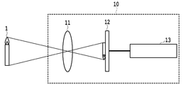
도 1은, 본 발명의 촬상장치의 개략 구성을 나타내는 측면도이다.
도 2는, 본 발명의 실시형태 1에 따른 촬상소자의 화소어레이 및 분광소자 어레이의 단면의 일부를 모식적으로 나타내는 도면이다.
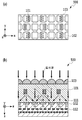
도 3에 있어서, (a)는 본 발명의 실시형태 1에 따른 촬상소자의 일부의 개략 구성의 상면도이고, (b)는 그 단면도이다.
도 4에 있어서, (a)는 본 발명의 실시형태 1에 따른 촬상소자의 미소분광소자를 구성하는 기둥상 구조체의 상면도이고, (b)는 그 단면도이다.
도 5에 있어서, (a)는 본 발명의 실시형태 1에 따른 촬상소자의 미소분광소자의 일례의 단면도이고, (b)는 미소분광소자에 의하여 분리된 3파장 각각의 위상지연분포를 나타내는 도면이다.
도 6에 있어서, (a)는 본 발명의 실시형태 1에 따른 촬상소자의 미소분광소자의 일례의 상면도이고, (b)는 그 단면도이다.
도 7에 있어서, (a)는 본 발명의 실시형태 1에 따른 촬상소자에 있어서, 기둥상 구조체의 상면으로부터 세로의 편광을 가지는 평행광을 입사하였을 때, 미소분광소자의 출사단으로부터 3방향으로 분리하여 전파하는 효율의 파장의존성을 나타내는 도면이고, (b)는 기둥상 구조체의 상면으로부터 세로의 편광을 가지는 평행광을 입사하였을 때, 미소분광소자의 출사단으로부터 3방향으로 분리하여 전파하는 효율의 파장의존성을 나타내는 도면이다.
도 8의 (a)~(h)는, 본 발명의 실시형태 1에 따른 촬상소자의 미소분광소자의 구조패턴예를 나타내는 도면이다.
도 9의 (a)~(c)는, 본 발명의 실시형태 1에 따른 촬상소자의 색성분에 대응하는 화소의 배치를 모식적으로 나타내는 도면이다.
도 10의 (a)~(c)는, 본 발명의 실시형태 1에 따른 촬상소자의 색성분에 대응하는 화소의 배치를 모식적으로 나타내는 도면이다.
도 11은, 본 발명의 실시형태 1의 변형예인 촬상소자의 개략 구성의 단면도를 나타낸다.
도 12에 있어서, (a)는 본 발명의 실시형태 2에 따른 촬상소자의 일부의 개략 구성의 상면도이고, (b)는 그 단면도이다.
도 13은, 본 발명의 실시형태 2에 따른 촬상소자의 화소의 배치를 모식적으로 나타내는 도면이다.
도 14에 있어서, (a)는 본 발명의 실시형태 3에 따른 촬상소자의 일부의 개략 구성의 상면도이고, (b)는 그 단면도이다.
도 15에 있어서, (a)는 본 발명의 실시형태 4에 따른 촬상소자의 일부의 개략 구성의 상면도이고, (b)는 그 단면도이다.
도 16은, 종래의 컬러촬상소자의 단면도이다.
도 17에 있어서, (a)는 종래의 분광소자를 이용한 컬러촬상소자의 상면도이고, (b)는 그 XVIIb-XVIIb 단면도이며, (c)는 그 XVIIc-XVIIc 단면도이다.
도 18은, 종래의 분광소자를 이용한 다른 컬러촬상소자의 단면도이다.1 is a side view showing a schematic configuration of an imaging device of the present invention.
2 is a diagram schematically showing a part of a cross section of a pixel array and a spectroscopic element array of an imaging device according to Embodiment 1 of the present invention.
In Fig. 3, (a) is a top view of a schematic configuration of a part of the imaging device according to Embodiment 1 of the present invention, and (b) is a cross-sectional view thereof.
In Fig. 4, (a) is a top view of a columnar structure constituting a microscopic spectral element of the imaging device according to Embodiment 1 of the present invention, and (b) is a cross-sectional view thereof.
In Fig. 5, (a) is a cross-sectional view of an example of the microscopic spectral element of the imaging device according to Embodiment 1 of the present invention, and (b) is a diagram showing the phase delay distribution of each of the three wavelengths separated by the microscopic spectral element. to be.
In FIG. 6, (a) is a top view of an example of a microscopic spectral element of the imaging device according to Embodiment 1 of the present invention, and (b) is a cross-sectional view thereof.
In Fig. 7, (a) in the image pickup device according to Embodiment 1 of the present invention, when parallel light having vertical polarization is incident from the top surface of the columnar structure, in three directions from the exit end of the microscopic spectral element. This is a diagram showing the wavelength dependence of the efficiency of propagating separately, and (b) is the efficiency of separating and propagating in three directions from the output end of the micro-spectral element when parallel light having vertical polarization is incident from the top surface of the columnar structure. It is a diagram showing the wavelength dependence of.
8 (a) to 8 (h) are diagrams showing examples of structural patterns of the microscopic spectral elements of the imaging element according to Embodiment 1 of the present invention.
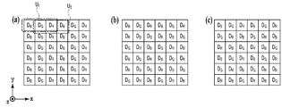
9A to 9C are diagrams schematically showing the arrangement of pixels corresponding to the color components of the image pickup device according to Embodiment 1 of the present invention.
10A to 10C are diagrams schematically showing the arrangement of pixels corresponding to the color components of the image pickup device according to Embodiment 1 of the present invention.
11 is a sectional view showing a schematic configuration of an image pickup device that is a modification of Embodiment 1 of the present invention.
In Fig. 12, (a) is a top view of a schematic configuration of a part of the imaging device according to Embodiment 2 of the present invention, and (b) is a cross-sectional view thereof.
13 is a diagram schematically showing the arrangement of pixels of an imaging device according to Embodiment 2 of the present invention.
In FIG. 14, (a) is a top view of a schematic configuration of a part of an imaging device according to a third embodiment of the present invention, and (b) is a cross-sectional view thereof.
In Fig. 15, (a) is a top view of a schematic configuration of a part of the imaging device according to Embodiment 4 of the present invention, and (b) is a cross-sectional view thereof.
16 is a cross-sectional view of a conventional color imaging element.
In Fig. 17, (a) is a top view of a color imaging device using a conventional spectroscopic element, (b) is a cross-sectional view of the XVIIb-XVIIb, and (c) is a cross-sectional view of the XVIIc-XVIIc.
18 is a cross-sectional view of another color imaging element using a conventional spectroscopic element.
이하, 도면을 이용하여 본 발명의 실시형태에 대하여 상세하게 설명한다. 단, 이하의 실시형태는 일례에 불과하고, 본 발명은 이들 실시형태로 한정되지 않는 것은 말할 것도 없다.EMBODIMENT OF THE INVENTION Hereinafter, embodiment of this invention is described in detail using drawing. However, the following embodiments are only examples, and it goes without saying that the present invention is not limited to these embodiments.
도 1은, 본 발명의 촬상장치의 개략 구성을 나타내는 측면도이다. 촬상소자(10)는, 렌즈광학계(11), CCD나 CMOS 등의 광전변환소자를 포함하는 촬상소자(12), 및 촬상소자(12)로부터 출력되는 광전변환신호를 처리하여 화상신호를 생성하는 신호처리부(13)를 구비한다.1 is a side view showing a schematic configuration of an imaging device of the present invention. The
자연광이나 조명광 등의 광이 물체(1)에 입사하고, 이것을 투과/반사/산란한 광은, 또는 물체(1)로부터 발하는 광은, 렌즈광학계(11)에 의하여 촬상소자(12) 상에 광학상을 형성한다. 일반적으로, 렌즈광학계(11)는, 다양한 광학수차를 보정하기 위하여, 광축을 따라서 늘어선 복수의 렌즈로 이루어지는 렌즈그룹에 의하여 구성되는데, 도 1에서는 도면을 개략화하여 단일 렌즈로서 나타내고 있다. 또한, 신호처리부(13)는, 생성한 화상신호를 외부로 송출하는 화상신호출력을 구비한다.Light such as natural light or illumination light enters the object 1, and light transmitted / reflected / scattered from the object 1 or light emitted from the object 1 is optically imaged on the
한편, 본 발명의 촬상장치(10)는, 적외광커트 광학필터, 전자셔터, 뷰파인더, 전원(전지), 플래시라이트 등의 공지의 구성요소를 구비할 수 있는데, 그들의 설명은 본 발명의 이해에 특별히 필요하기 않기 때문에 생략한다. 또한, 이상의 구성은 어디까지나 일례이며, 본 발명에 있어서 렌즈광학계(11), 촬상소자(12), 신호처리부(13)를 제외하는 구성요소에는, 공지의 요소를 적절히 조합하여 이용할 수 있다.On the other hand, the
본 발명의 구체적인 실시형태를 설명하기 전에, 본 발명의 실시형태에 있어서의 촬상소자(12)의 개략을 설명한다.Before explaining the specific embodiment of the present invention, the outline of the
본 발명의 실시형태에 따른 촬상소자(12)는, 광전변환소자를 포함하는 셀(화소)(102)이 2차원상으로 복수 배열된 화소어레이와, 미소분광소자(101)가 2차원상으로 복수 배열된 분광소자 어레이를 구비한다. 도 2는, 본 발명의 실시형태 1에 따른 촬상소자의 화소어레이 및 분광소자 어레이의 단면의 일부를 모식적으로 나타내는 도면이다. 분광소자 어레이는 화소어레이와 대향하고 있고, 렌즈광학계로부터의 광이 입사하는 측에 배치되어 있다. 각 미소분광소자(101)는 두께가 일정한 복수의 기둥상 구조체로 구성되어 있다. 한편, 미소분광소자(101)는, 편의상 4개의 기둥상 구조체로 나타나고 있는데, 개수나 간격, 배열패턴에 제한은 없으며, 다양한 배열형태를 취할 수 있다.In the
촬상소자(12)에 입사하는 광에 포함되는 가시광성분을, 파장영역마다 제1 색성분, 제2 색성분, 제3 색성분으로 분류한다. 한편, 제1 내지 제3 색성분의 조합은, 일반적으로 적(R), 녹(G), 청(B)의 3원색의 조합인데, 광을 3개의 파장역으로 나누는 것이라면 이것으로 한정되지 않는다.The visible light components included in the light incident on the
본 발명의 실시형태에 있어서의 미소분광소자(101)는, 후술하는 위상지연효과 및 그 구조치수의존성·파장의존성을 이용함으로써, 상술한 제1 내지 제3 색성분에 따라서, 입사한 광의 전파방향을 바꾸고, 화소어레이 상에 있어서 공간적으로 분리하는 기능을 갖는다. 즉, 본 발명의 실시형태에서는, 촬상소자에 입사한 광의 적어도 일부의 광이, 미소분광소자(101)에 의하여, 색성분에 따라서 전파방향을 바꾸고, 복수의 화소(102)에 입사한다. 따라서, 미소분광소자(101)와 화소(102)의 거리를 적절하게 설정함으로써, 3개의 파장역으로 분리된 광을 각각 다른 화소(102)로 받는 것이 가능하다.The microscopic
화소(102)에 광이 입사하면, 광전변환소자에 의하여 입사한 광의 감도에 따른 전기신호(광전변환신호)를 출력하기 때문에, 색성분에 따른 신호(컬러정보)를 직접적으로 또는 신호연산을 이용하여 취득할 수 있다. 이상의 미소분광소자(101) 및 미소분광소자(101)에 대응한 복수의 화소(102)가 2차원상으로 배치되어 있으므로, 렌즈광학계(11)에 의하여 형성되는 물체의 광학상의 컬러정보를 취득할 수 있다.When light enters the
후술하는 실시형태 1 및 실시형태 2에 대하여는, 마이크로렌즈 어레이를 이용함으로써, 입사광의 거의 모두가 분광소자 어레이를 구성하는 어떤 미소분광소자(101)를 투과하므로, 입사광의 거의 모두가 3개의 파장역으로 분리된 상태로 화소어레이에 입사한다. 따라서, 광전변환신호로부터 직접적으로 또는 간이한 연산을 이용하여 컬러정보를 취득할 수 있다.In the first and second embodiments described later, by using a microlens array, almost all of the incident light passes through some
후술하는 실시형태 3 및 실시형태 4에 대하여는, 입사광의 일부가 분광소자 어레이를 구성하는 미소분광소자(101)를 투과하므로, 입사광의 일부가 3개의 파장역으로 분리된 상태로 화소어레이에 입사한다. 따라서, 각 화소(102)의 일부는, 3개의 파장역으로 분리된 상태의 광과 분리되어 있지 않은 상태의 광의 합산의 광강도에 따른 광전변환신호를 출력한다. 출력된 광전변환신호에 대하여, 후술하는 적절한 행렬연산을 이용함으로써, 컬러정보를 구할 수 있다.In the third and fourth embodiments described later, a part of the incident light passes through the microscopic
본 발명의 실시형태에 있어서의 촬상소자(12)에 따르면, 감색형의 색필터를 이용하지 않고, 미소분광소자(101)를 이용한 3색으로의 저손실 광분리에 의하여, 컬러정보를 얻을 수 있다. 따라서, 색필터를 이용한 촬상소자와 비교하여, 화소어레이에 도달하는 광총량을 증가시킬 수 있어, 촬상감도를 높이는 것이 가능해진다. 더욱이, 미소분광소자(101)는 제작이 간이한 두께가 일정한 구조체로 구성되어 있고, 또한 구조체 상면·바닥면의 대칭성으로부터 편광의존성이 발생하지 않는 것으로부터, 비특허문헌 1에서 개시된 종래 기술에 있어서의 색분리기능에 편광의존성이 존재한다는 과제를 해결할 수 있다.According to the
이하, 도면을 참조하면서, 본 발명의 보다 구체적인 실시형태를 설명한다.Hereinafter, more specific embodiment of this invention is described, referring drawings.
(실시형태 1)(Embodiment 1)
이하, 본 실시형태 1에 있어서의 촬상소자의 구성의 개략에 대하여 설명한다.Hereinafter, an outline of the configuration of the imaging element in the first embodiment will be described.
도 3의 (a)는 본 발명의 실시형태 1에 따른 촬상소자의 일부의 개략 구성의 상면도이고, 도 3의 (b)는 그 단면도이다. 본 실시형태 1에 있어서의 촬상소자(100)는, 광전변환소자를 포함하는 화소(102)가 어레이상이 되도록 배열된 2차원 화소어레이 상에, SiO2 등으로 이루어지는 저굴절률의 투명층(111), 복수의 마이크로렌즈(103)가 적층되어 있다. 저굴절률의 투명층(111)의 내부에는, 투명층(111)의 굴절률보다 높은 굴절률을 가지는 SiN 등의 재료로 형성된 복수의 두께(2차원 화소어레이에 대하여 수직방향의 길이)가 일정한 미세구조체로 이루어지는 미소분광소자(101)가 매립되어 있다. 편의상, 이하의 설명에 있어서, 2차원 화소어레이의 법선방향을 z축, 2차원 화소어레이에 평행하고, 화소유닛(110)을 구성하는 3개의 화소(102)가 늘어서는 방향을 x축, 2차원 화소어레이에 평행하고 x축과 직교하는 방향을 y축으로 하는 xyz 직교좌표계를 설정한다.3A is a top view of a schematic configuration of a part of an imaging device according to Embodiment 1 of the present invention, and FIG. 3B is a cross-sectional view thereof. The
도면에 나타나 있는 바와 같이, 마이크로렌즈(103), 미소광학소자(101), 화소(102)는 xy 평면상에 있어서 격자상으로 배치되어 있고, 각 마이크로렌즈(103)의 중심축 상에 1개의 미소분광소자(102)가 배치되어 있다. x축 방향으로 이웃하는 3개의 화소를 1개의 화소유닛(110)으로 하면, x축 방향으로 이웃하는 각 마이크로렌즈(103)는 각각 화소유닛(110)과 1대1로 대응하고, 각 마이크로렌즈(103)의 중심축은 대응하는 화소유닛의 중앙의 화소(102)의 거의 중심을 통과한다. 즉, x축 방향으로 이웃하는 3개의 화소(102)에 대하여 1개의 마이크로렌즈(103) 및 1개의 미소분광소자(101)가 대응하고 있고, 상기의 마이크로렌즈(103), 미소분광소자(101), 화소유닛(110)을 1개의 촬상소자유닛으로 하면, 그 촬상소자유닛이 xy 평면상에 있어서 격자상으로 배열되어 있다.As shown in the figure, the
한편, 상술한 설명에서는, 일례로서, 직교격자상으로 배열된 2차원 화소어레이의 경우에 대하여 설명하였는데, 화소(102)의 배열, 형상, 사이즈 등은 이러한 도면의 예로 한정되지 않으며, 공지의 어떠한 배열, 형상, 사이즈여도 좋다. 또한, 도 3의 (a), (b)에서는 생략하고 있는데, 2차원 화소어레이와 미세구조체 사이에, 내부 마이크로렌즈로서 동작하고, 미소분광소자(101)로부터의 광을 화소(102) 내의 광전변환소자로 안내하는 작용을 하는 SiN 등으로 이루어지는 고굴절률의 요철구조를 구비할 수 있다. 도 3의 (a), (b)에 나타나는 구조는, 공지의 반도체 제조기술에 의하여 제작될 수 있다.On the other hand, in the above description, as an example, the case of a two-dimensional pixel array arranged in an orthogonal grid has been described, but the arrangement, shape, size, etc. of the
한편, 도 3의 (a), (b)에 나타나는 촬상소자(100)는, 배선층(112)의 반대측으로부터 수광하는 이면조사형의 구조인데, 본 실시형태에서는 이와 같은 구조로 한정되지 않으며, 배선층(112)의 측으로부터 수광하는 표면조사형의 구조를 가지고 있어도 좋다.On the other hand, the
이하, 본 실시형태에 있어서의 촬상소자(100)의 각 구성요소의 작용에 대하여 설명한다.Hereinafter, the operation of each component of the
촬상소자(100)에 입사하는 백색의 광은, 우선 마이크로렌즈 어레이에 의하여 집광되고, 거의 모든 광이 각 마이크로렌즈(103)에 대응한 미소분광소자(101)를 통과한다. 각 미소분광소자(101)에 의하여, 광은 xz면 내에서 3파장역으로 공간적으로 분리되고, 각 미소분광소자(101)의 바로 밑에 있는 3화소(102)에 의하여 각각 수광된다. 도 3의 (b)에 나타내는 예에서는, 각 미소분광소자(101)에 의하여, 제1 색성분의 광(R)이 제1 방향(우)으로, 제2 색성분의 광(G)이 제2 방향(직진)으로, 제3 색성분의 광(B)이 제3 방향(좌)으로 전파되고 있으므로, 각 미소분광소자(101) 바로 밑의 3화소(102, (DR(우), DG(중앙), DB(좌)))가 각각 R, G, B의 컬러정보의 검출에 대응한다.The white light incident on the
한편, 상술은 일례이며, 각 미소분광소자(101)의 구성에 따라서는, 색성분과 전파방향의 조합은 자유롭게 변경 가능하고, 그에 따라서 RGB 각각에 대응하는 화소(102(DR, DG, DB))도 변경된다.Meanwhile, the above is an example, and depending on the configuration of each microscopic
이와 같이 3파장역으로 공간적으로 분리된 광이 3화소(102)에 의하여 각각 수광되면, 각 화소(102) 내의 광전변환소자에 의하여 광전변환이 이루어지고, 컬러정보를 포함하는 화상신호가 출력된다.When light spatially separated into three wavelengths is received by the three
한편, 각 미소분광소자(101)의 바로 밑에 있는 3화소(102(DR, DG, DB))의 x축 방향의 폭(wd1, wd2, wd3)은, 동일하여도 좋고 달라도 좋다. 또한, 이에 따라서, 마이크로렌즈(103)의 x축 방향의 폭(wlx)과 y축 방향의 폭(wly)은 동일하여도 좋고 달라도 좋다. 도 3의 예에서는, 3화소(102(DR, DG, DB))의 x축 방향의 폭(wd1, wd2, wd3)이 동일하고, 마이크로렌즈(103)는 wlx와 wly는 다르다.On the other hand, the width (w d1 , w d2 , w d3 ) in the x-axis direction of the three pixels 102 (D R , D G , D B ) directly under each microscopic
또한, 화소유닛(110)과 미소분광소자(101) 사이에는, 내부 마이크로렌즈로서 동작하는 SiN 등으로 이루어지는 고굴절률의 요철구조를 구비할 수 있는데, 후술하는 미소분광소자(101)는 형성하는 위상지연분포에 따라서는, 렌즈기능을 가지는 것이 가능하므로, 내부 마이크로렌즈를 생략하는 것도 가능하다.Further, between the
이하, 본 실시형태에 있어서의 미소분광소자에 대하여 설명한다.Hereinafter, the microscopic spectral element in this embodiment will be described.
본 실시형태 1에 있어서의 미소분광소자(101)는, 복수의 미세한 기둥상 구조체(121)로 구성된다. 도 4의 (a)는 본 발명의 실시형태 1에 따른 촬상소자의 미소분광소자를 구성하는 기둥상 구조체의 상면도이고, 도 4의 (b)는 그 단면도이다. 기둥상 구조체(121)는, 투명층(111)의 굴절률(n0)보다 높은 굴절률(n1)을 가지는 SiN 등의 재료로 형성되어 있고, 구조의 두께(h)는 일정하다.The microscopic
또한, 기둥상 구조체(121)의 바닥면 및 상면은 정방형이다. 이러한 기둥상 구조체(121)는, 투명층(111)과의 굴절률차로부터, 광을 구조 내에 가두어서 전파시키는 광도파로로서 기능한다. 따라서, 상면측으로부터 광을 입사하면, 광은 기둥상 구조체(121) 내에 단단히 가두어진 채 전파되고, 광도파로의 실효적인 굴절률(neff)에 의하여 결정되는 위상지연효과를 받아, 바닥면측으로부터 출력된다. 구체적으로, 투명층(111)을 기둥상 구조체(121)의 두께만큼의 길이를 전파한 광의 위상을 기준으로 하였을 때, 기둥상 구조체(121)에 의한 위상지연량(ø)은, 광의 진공 중에서의 파장을 λ로 두면,In addition, the bottom surface and the top surface of the
ø=(neff-n0)×2πh/λ (1)ø = (n eff -n 0 ) × 2πh / λ (1)
로 나타난다. 이러한 위상지연량은 광의 파장(λ)에 따라서 다르기 때문에, 동일한 기둥상 구조체(121)에 입사한 광에 대하여 파장역(색성분)에 따라서 다른 위상지연량을 줄 수 있다. 그리고, 기둥상 구조체(121)의 바닥면 및 상면이 정방형이므로, 편광방향을 바꾼 경우에도, 위상지연효과를 포함하는 광학특성에 변화는 없다. 더욱이, neff는 구조치수의 함수인 것이 알려져 있고, n0<neff<n1의 값을 취한다. 따라서, 도 4의 (a), (b)에 나타내는 예에서는, 기둥상 구조체(121)의 폭(w)을 변화시킴으로써, 임의의 위상지연량을 설정하는 것이 가능하다.Appears as Since the amount of phase delay varies depending on the wavelength (λ) of light, it is possible to give a different amount of phase delay according to the wavelength range (color component) for light incident on the same pillar-shaped
도 5의 (a)의 단면도는, x축 방향으로 상술한 기둥상 구조체(121-1, 121-2)를 2개 나열하여 구성한, 본 실시형태 1에 있어서의 미소분광소자(101)의 일례이다. 한편, y축 방향으로는, 파장 이하의 간격으로, 상술한 기둥상 구조체(121-1, 121-2)가 복수 늘어서 있다.5 (a) is an example of the microscopic
도 5의 (a)에 나타내는 바와 같이, x축 방향으로 인접하는 기둥상 구조체(121-1, 121-2)의 폭(w)이 다르다. 이러한 폭(w)의 차이에 의하여, 미소분광소자(101)를 투과한 광에 대하여, 파장영역마다 다른 위상지연분포를 주는 것이 가능해져, 광파면을 변화시킬 수 있다. 광의 전파방향(편향방향)은 이러한 광파면에 의하여 결정되므로, 미소분광소자(101)를 투과한 광을 파장역(색성분)에 따라서 공간적으로 분리하는 것이 가능해진다. 즉, 본 실시형태 1에 있어서의 미소분광소자(101)는, 복수의 기둥상 구조체(121)를 배치하고, 인접하는 기둥상 구조체(121-1, 121-2)의 광의 전파방향과 직교하는 면에 있어서의 치수(w)를 변화시킴으로써, 입사광의 파장영역에 따라서 다른 광파면을 주어, 색성분을 공간적으로 분리한다.As shown in Fig. 5A, the widths w of the columnar structures 121-1 and 121-2 adjacent in the x-axis direction are different. Due to the difference in the width w, it is possible to provide a different phase delay distribution for each wavelength region with respect to the light transmitted through the microscopic
예를 들어, 도 5의 (a)에 나타내는 구조의 경우, 도 5의 (b)에 나타내는 바와 같이, 3파장(예를 들어, RGB에 대응하는 파장)에 따라서 다른 위상지연분포를 줄 수 있다. 이러한 예에서는, 제1 색성분의 광(R)에 대응하는 파장의 위상지연분포는 위상량이 0에서 +2π까지 선형 증가하는 직선 상을 따르고 있고, 제2 색성분의 광(G)에 대응하는 파장의 위상지연분포는 공간적인 변화는 없으며, 제3 색성분의 광(B)에 대응하는 파장의 위상지연분포는 위상량이 0에서 -2π까지 선형 감소하는 직선 상을 따르고 있다. 이러한 경우, 미소분광소자(101)를 투과한 광은, 도 5의 (a)에 나타내는 바와 같이, 제1 색성분의 광(R)이 제1 방향(우)으로, 제2 색성분의 광(G)이 제2 방향(직진)으로, 제3 색성분의 광(B)이 제3 방향(좌)으로 각각 효율적으로 전파될 수 있다. For example, in the case of the structure shown in Fig. 5 (a), as shown in Fig. 5 (b), a different phase delay distribution can be given according to 3 wavelengths (for example, a wavelength corresponding to RGB). . In this example, the phase delay distribution of the wavelength corresponding to the light R of the first color component follows a linearly increasing phase amount from 0 to + 2π, and of the wavelength corresponding to the light G of the second color component. The phase delay distribution has no spatial change, and the phase delay distribution of the wavelength corresponding to the light B of the third color component follows a linear phase in which the phase amount linearly decreases from 0 to -2π. In this case, as for light passing through the microscopic
한편, 상술한 설명은 일례로서, 각 기둥상 구조체(121)의 치수에 따라서는, 색성분과 편향방향의 조합은 자유롭게 변경 가능하다. 예를 들어, 제1 색성분의 광(R)이 제2 방향(직진)으로, 제2 색성분의 광(G)이 제1 방향(우)으로, 제3 색성분의 광(B)이 제3 방향(좌)으로 각각 효율적으로 전파될 수 있다.On the other hand, the above description is an example, and depending on the dimensions of each
본 실시형태에 있어서의 미소분광소자(101)의 보다 상세한 일례를 설명한다.A more detailed example of the microscopic
도 6의 (a)는 본 발명의 실시형태 1에 따른 촬상소자의 미소분광소자의 일례의 상면도이고, 도 6의 (b)는 그 단면도이다. x축 방향으로는 서로 다른 폭(w1, w2)을 가지는 두께(2차원 화소어레이에 대하여 수직방향의 길이)가 일정한 기둥상 구조체(121-1, 121-2)가 2개 늘어서 있고, y축 방향으로는 동일한 기둥상 구조체(121-1, 121-2)가 3개 늘어서 있으며, 이상을 1개의 미소분광소자(101)로 한다. 한편, 기둥상 구조체(121-1, 121-2)를 구성하는 재료는 SiN(n1=2.03)을 상정하고, 투명층을 구성하는 재료는 SiO2(n0=1.45)를 상정하며, 바닥면 및 상면이 정방형인 경우를 나타내고 있다. 또한, 모든 기둥상 구조체(121-1, 121-2)의 두께(h)를 1200nm, 패턴 좌측의 기둥상 구조체(121-1)의 폭(w1)을 145nm, 패턴 우측의 기둥상 구조체(121-2)의 폭(w2)을 340nm로 하고, x축 및 y축 방향에 있어서의 기둥상 구조체(121-1, 121-2)의 간격(p)은 450nm로 하였다.Fig. 6A is a top view of an example of the microscopic spectral element of the image pickup device according to Embodiment 1 of the present invention, and Fig. 6B is a sectional view thereof. in the x-axis direction and different widths (w 1, w 2) having the thickness (the length of the two-dimensional direction perpendicular to the pixel array) is a constant columnar structures (121-1, 121-2) is lined with two, In the y-axis direction, three identical columnar structures 121-1 and 121-2 are lined up, and the above is referred to as one microscopic
도 7의 (a), (b)에, 상술한 구조에 있어서, 기둥상 구조체(121-1, 121-2)의 상면으로부터 평행광을 입사하였을 때, 미소분광소자(101)의 출사단으로부터 3방향(도 6의 (b)의 R, G, B의 각 방향)으로 분리하여 전파하는 효율(입사광 강도에 대한 각 전파방향의 광강도의 비)의 파장의존성(엄밀결합파 이론에 근거하는 계산결과)을 나타낸다. 도 7의 (a)는, 도 6의 (a) 중의 세로의 편광을 가지는 광, 도 7의 (b)는 도 6의 (a) 중의 가로의 편광을 가지는 광을 각각 입사하였을 때의 결과이다. 한편, 계산시, 상술한 미소분광소자(101)가 x축 y축 방향에 있어서 P의 간격(P=3p)으로 늘어서 있다고 가정하였는데, 단독체의 미소분광소자(101)에 있어서의 광학기능과의 차이는 거의 없는 것을 확인하고 있다. 또한, 3방향의 각각의 편향각(θR, θG, θB)은, 광의 회절에 근거하고 있으며, R:sinθR=λ/P, G:θG=0(직진), B:sinθB=λ/P로 하였다.7 (a) and 7 (b), in the above-described structure, when parallel light is incident from the upper surfaces of the columnar structures 121-1 and 121-2, from the exit end of the microscopic
또한, 도 7의 (a), (b)에 나타낸 특성은, 종래의 촬상장치에 있어서의 색필터의 분광감도특성에 상당한다. 도 7의 (a), (b)에 나타내는 결과는, 제1 방향(R)에 있어서의 효율은 600nm 이상의 적색파장역에서 피크를 이루고, 제2 방향(G)에 있어서의 효율은 500~600nm의 녹색파장역에서 피크를 이루며, 제3 방향(B)에 있어서의 효율은 500nm 이하의 청색파장역에서 피크를 이루고 있는 것을 나타내고 있다. 또한, 40~60%라는 양호한 분광성능을 나타내고 있고, 또한 특성에 큰 편광의존성은 보이지 않는다. 한편, 곡선 R, G, B의 총합, 즉 총투과율은 95% 이상이고, 산란이나 반사에 따른 광손실은 거의 발생하지 않는다.Note that the characteristics shown in Figs. 7A and 7B correspond to the spectral sensitivity characteristics of the color filter in the conventional imaging device. The results shown in Figs. 7A and 7B show that the efficiency in the first direction R peaks in the red wavelength region of 600 nm or more, and the efficiency in the second direction G is 500 to 600 nm. The peak is formed in the green wavelength range of, and the efficiency in the third direction (B) is peaked in the blue wavelength range of 500 nm or less. In addition, it shows good spectral performance of 40 to 60%, and does not show a large polarization dependency on the properties. On the other hand, the total sum of the curves R, G, and B, that is, the total transmittance is 95% or more, and light loss due to scattering or reflection hardly occurs.
이상의 결과는, 본 실시형태 1에 있어서의 미소분광소자(101)를 이용함으로써, 색성분의 고효율의 공간적인 분리가 가능하다는 것을 나타내고 있다. 더욱이, 상술한 예에서는, 단독체의 미소분광소자(101)의 사이즈는 1.35㎛각이고, 일반적인 CCD 및 CMOS 센서의 최소 픽셀 사이즈와 동등하다. 따라서, 최소 픽셀 사이즈를 가지는 화소유닛(110)에 대응한 미소분광소자(101)의 형성이 가능하다. 한편, 기둥상 구조체(121)의 사이즈나 개수, 배열패턴에 따라서 다른 사이즈의 미소분광소자(101)를 형성하는 것도 가능하다.The above results indicate that the highly efficient spatial separation of color components is possible by using the microscopic
미소분광소자(101)를 구성하는 기둥상 구조체(121)의 재료, 개수, 형상, 사이즈, 배열패턴 등을 적절하게 설계함으로써, 원하는 분광특성을 주는 것이 가능하다. 그 결과, 상술한 바와 같이, 각각의 광전변환소자에 원하는 파장역의 광만을 분리하여 입사시키는 것이 가능해져, 각 광전변환소자로부터 출력되는 광전변환신호로부터, 색성분에 대응하는 신호를 취득할 수 있다.By appropriately designing the material, number, shape, size, and arrangement pattern of the
또한, 상술과 같이, 미소분광소자(101)에 따른 광손실은 거의 발생하지 않기 때문에, 종래 기술의 색필터를 이용한 촬상소자와 비교하여, 화소어레이에 도달하는 광총량을 비약적으로 증가시킬 수 있어, 촬상감도를 높이는 것이 가능해진다. 한편, 각 미소분광소자(101)의 분광성능이 상술한 이상적인 성능과 다소 달라도, 성능의 차이의 정도에 따라서, 취득한 신호를 보정·연산하는 것에 의하여 양호한 색정보를 얻는 것이 가능하다.In addition, as described above, since the light loss due to the microscopic
또한, 상술한 각 기둥상 구조체(121)의 배치에 있어서, 주기적인 구조에 기인하는 불필요한 회절광이 발생하는 것을 방지하기 위하여, 광의 파장 이하의 간격으로 배치하는 것이 바람직하다.In addition, in the arrangement of each of the pillar-shaped
상술한 예에서는, 기둥상 구조체의 바닥면 및 상면이 정방형인 경우에 대하여 설명하였는데, 이러한 형상으로 한정되지 않는다. 즉, 바닥면 및 상면의 중심을 통과하는 축을 대칭축으로서 4회 회전대칭이 되는 형상면이라면, 분광기능의 편광에 대한 의존성이 발생하지 않고, 위상지연효과를 초래하는 광도파로로서의 동작도 손실되는 일은 없다. 따라서, 도 8의 (a)~(h)에 나타내는 바와 같은 정방형, 중공정방형, 원형, 중공원형, 십자형상 등의 4회 회전대칭이 되는 면을 가지는 기둥상 구조체를 채용하는 것이 바람직하다.In the above-described example, the case where the bottom and top surfaces of the columnar structure are squares has been described, but is not limited to such a shape. That is, if the axis passing through the centers of the bottom surface and the top surface is a symmetrical axis and is a rotational symmetry 4 times, the dependency on the polarization of the spectral function does not occur, and the operation as an optical waveguide causing a phase delay effect is also lost. none. Therefore, it is preferable to adopt a columnar structure having a surface which becomes four times rotationally symmetrical, such as a square, a middle process square, a circular shape, a hollow shape, and a cross shape, as shown in Figs. 8A to 8H.
한편, 미소분광소자(101)에 따른 색성분의 분리 후에 있어서, 화소유닛(110) 상의 각 광공간분포가 서로 충분히 분리하기 위하여는, 미소분광소자(101)의 출력단과 화소(102)의 광전변환소자와의 사이가 1㎛ 이상의 간격인 것이 바람직하다. 한편으로, 촬상소자(100)의 박막화 및 재료비·프로세스 시간의 절약을 위하여, 상술한 미소분광소자(101)의 출력단과 화소(102)의 광전변화소자와의 간격은, 가능한 한 짧은 편이 바람직하다.On the other hand, after separation of the color components according to the microscopic
또한, 이 경우, 짧은 전파거리로, 화소유닛(110) 상의 각 광공간분포가 색성분에 따라서 서로 확실히 분리될 필요가 있으므로, 미소분광소자(101)에 의하여 광의 파면을 크게 기울이고, 편향하는(구부리는) 각도를 크게 하는 것이 바람직하다. 편향하는 각도를 크게 하기 위하여는, 미소분광소자(101)에 의하여 형성되는 각 파장역에 있어서의 위상지연분포가 각각 0에서 2π까지 변화하는 형태가 적합하기 때문에, 각각의 파장역에 있어서, 기둥상 구조체(121)에 따른 위상지연량의 가변범위는, 2π 이상 가지고 있는 것이 바람직하다. 따라서, 식 (1)로부터, 분리하는 파장역의 가장 긴 파장측의 파장역에 있어서의 원하는 중심파장을 λr로 하면, 기둥상 구조체(121)의 두께(h)는, h=λr/(n1-n0)의 근방으로 설정하는 것이 바람직하다.In addition, in this case, since the optical space distribution on the
이상과 같은 분광기능을 가지는 미소분광소자(101)는, 공지의 반도체 제조기술에 의하여, 박막퇴적 및 패터닝을 실행함으로써 제작할 수 있다. 본 실시형태 1의 미소분광소자(101)는, 복수의 두께가 일정한 기둥상 구조체(121)로 구성되므로, 비특허문헌 1에서 개시되어 있는 계단상 구조 등과 비교하여, 저렴하고 쉽게 제작할 수 있다.The microscopic
이하, 본 실시형태의 촬상소자에 있어서의 미소광학소자 및 화소의 배치에 대하여 설명한다.Hereinafter, the arrangement of the micro-optical elements and pixels in the imaging element of the present embodiment will be described.
도 3에 나타낸 일례에서는, x축 방향을 따라서 배치된 미소분광소자(101)의 행이, x축 방향으로 어긋나지 않고 y축 방향을 따라서 반복 배치되어 있으며, 그 결과, y축 방향을 따라서 미소분광소자(101)의 패턴이 연속적으로 배치되어 있다. 이 경우, x축 방향에 있어서는, 각 미소분광소자(101) 바로 밑의 색성분에 대응하는 3화소(102(DR, DG, DB))가 좌측에서부터 이 순서대로 나열되고, 이 나열이 반복 배치되어 있다.In the example shown in FIG. 3, the rows of the microscopic
더욱이, 화소(102)에 대하여도 마찬가지로, x축 방향을 따라서 배치된 화소(102)의 행이, x축 방향으로 어긋나지 않고 y축 방향을 따라서 반복 배치되어 있으며, 그 결과 y축 방향을 따라서 3화소(102(DR, DG, DB))가 각각 연속적으로 배치되어 있다.Moreover, similarly to the
도 9의 (a)~(c)는, 본 발명의 실시형태 1에 따른 촬상소자의 색성분에 대응하는 화소의 배치를 모식적으로 나타낸 것이다. x축 방향으로 이웃하는 3개의 화소(102(DB, DG, DR))를 1개의 컬러화소유닛(U)으로 하면, 도 9의 (a)에 나타내는 컬러화소유닛(U1), 및 컬러화소유닛(U1)에 대하여 단일화소만큼 x축 방향으로 시프트한 컬러화소유닛(U2)은, 모두 R, G, B에 대응하는 화소를 반드시 1개씩 포함하게 된다. 즉, 컬러화소유닛(U)을 xy평면에 있어서 단일화소씩 시프트하면서, 컬러정보 취득하면, RGB 3색의 정보를 거의 화소수만큼 얻을 수 있다. 이것은, 촬상소자의 해상도를 화소수의 정도까지 높일 수 있다는 것을 의미하고 있다(이른바, 베이어 배치와 동등함). 따라서, 본 실시형태 1의 촬상소자는, 고감도인 것과 더불어, 단일화소 사이즈의 고해상도로 컬러정보를 생성할 수 있다.9A to 9C schematically show the arrangement of pixels corresponding to the color components of the image pickup device according to Embodiment 1 of the present invention. When three pixels 102 (D B , D G , D R ) neighboring in the x-axis direction are used as one color pixel unit U, the color pixel unit U 1 shown in FIG. 9 (a), and a color pixel unit color pixel unit (U 2) a shift in the x-axis direction by one pixel with respect to the (U 1) is contained will be one at all the pixels corresponding to R, G, B. That is, if color information is acquired while the color pixel unit U is shifted by one pixel on the xy plane, information of three colors of RGB can be almost obtained by the number of pixels. This means that the resolution of the imaging device can be increased to the level of the number of pixels (so-called equivalent to Bayer arrangement). Therefore, the imaging device of the first embodiment can generate color information with high sensitivity and high resolution of a single pixel size.
상술과 같은 단일화소 사이즈의 해상도를 실현하는 미소광학소자 및 화소의 배치는, 도 9의 (a)로 한정되지 않으며, 다양하게 변경할 수 있다. 도 9의 (b) 및 도 9의 (c)는, 다른 예를 나타내고 있고, x축 방향을 따라서 구성되는 미소분광소자(101) 및 컬러화소유닛(U)의 행이, 도 9의 (b)에서는 1화소 사이즈만큼, 도 9의 (c)에서는 2화소 사이즈만큼, x축 방향으로 시프트하면서 순차 y축 방향으로 배치되어 있다. 이와 같은 배치에 대하여도, 도 9의 (a)와 마찬가지로 단일화소 사이즈의 해상도로 컬러정보를 생성할 수 있다.The arrangement of the micro-optical elements and pixels for realizing the resolution of the single pixel size as described above is not limited to FIG. 9 (a) and can be variously changed. 9 (b) and 9 (c) show another example, and the rows of the microscopic
도 10의 (a)~(c)는, 도 9의 (a)~(c)와는 다른 배치의 예를 나타내고 있고, 행마다 3화소(DB, DG, DR)의 순번이 반전되는 구성이며, x축 방향으로 시프트에 대하여는 상술하는 도 9의 (a)~(c)와 각각 마찬가지이다. 이 경우에 대하여도, 도 9의 (a)와 마찬가지로 단일화소 사이즈의 해상도로 컬러정보를 생성할 수 있다. 한편, 3화소(DB, DG, DR)의 순번의 반전을 행하기 위하여는, 상술하는 미소분광소자(101)의 기둥상 구조체(121-1, 121-2)를 x축에 있어서 좌우 반전시킨 패턴을 이용하면 좋다.10 (a) to 10 (c) show examples of arrangement different from those of FIGS. 9 (a) to 10 (c), and the sequence numbers of three pixels (D B , D G , and D R ) are reversed for each row. It is a configuration, and the shifts in the x-axis direction are the same as in Figs. 9A to 9C described above. Also in this case, color information can be generated with a resolution of a single pixel size as in Fig. 9A. On the other hand, in order to reverse the sequence of the three pixels (D B , D G , D R ), the columnar structures 121-1 and 121-2 of the microscopic
상술한 도 9의 (a)~(c) 및 도 10의 (a)~(c)에 나타내는 화소배치는, 입사광이 각 미소분광소자(101)의 기능에 의하여, 제1 색성분의 광(R)이 제1 방향(우)으로, 제2 색성분의 광(G)이 제2 방향(직진)으로, 제3 색성분의 광(B)이 제3 방향(좌)으로 전파되고, 각 미소분광소자(101) 바로 밑의 3화소(102(DR(우), DG(중앙), DB(좌)))가 각각 R, G, B의 컬러정보의 검출에 대응한다고 상정하였을 때의 것이다. 상술한 바와 같이, 미소분광소자(101)의 구성에 의하여는, 미소분광소자(101) 바로 밑의 화소(102)가 RGB 3색의 어느 것에 대응한 것이 되는지 변하는데, 기본적으로는 컬러화소유닛(U) 내의 순번이 변경될 뿐이다. 그와 같은 경우에 대하여도, 도 9 및 도 10에 나타낸 컬러화소유닛(U)의 배치규칙에 따라서, 배치를 설정하면, 마찬가지로 단일화소 사이즈의 해상도로 컬러정보를 생성할 수 있다.In the pixel arrangement shown in FIGS. 9A to 9C and 10A to 10C, the incident light is the first color component light R due to the function of each microscopic spectral element 101. ) In the first direction (right), light (G) of the second color component in the second direction (straight), light (B) of the third color component propagates in the third direction (left), and each microspectral element (101) It is assumed that the three pixels (D R (right), D G (center), D B (left)) immediately below correspond to detection of color information of R, G, and B, respectively. . As described above, depending on the configuration of the microscopic
이상의 설명에서는, 미소분광소자(101)만을 이용한 경우의 촬상소자(100)에 대하여 서술하였다. 다음으로, 감색형의 색필터를 병용하였을 때의 변형예에 대하여 설명한다.In the above description, the
도 11에, 본 발명의 실시형태 1의 변형예인 촬상소자의 개략 구성의 단면도를 나타낸다. 도 3과의 차이는, 색성분에 대응한 화소(102)이 상방에, 화소(102)의 색에 각각 대응한 색필터(104)를 배치하고 있는 점이고, 그 밖에는 동일하다. 이러한 구성의 경우, 종래 기술의 색필터만인 구성에 비하여, 광이용 효율이 향상되고, 또한 색재현성도 향상된다.11 shows a cross-sectional view of a schematic configuration of an imaging device that is a modified example of Embodiment 1 of the present invention. The difference from FIG. 3 is that the
예를 들어, 도 7로부터, 미소분광소자(101)의 RGB로의 분광효율은 40~60%로 한다. 또한, RGB의 색필터(104)의 대응하는 파장역에 있어서의 투과율(분광효율)을 각각 90%로 한다. 입사광이 RGB 1:1:1의 비율의 강도를 가지고 있다고 한다. 이 경우, 미소분광소자(101)와 색필터(104)를 병용한 경우에서는, 광이 양자를 투과하여 화소에 입사하기 때문에, RGB 3화소(102)에 도달하는 광강도의 총량은 36~54%가 된다. 더욱이, 미소분광소자(101) 및 색필터(104)의 분광성능이 곱해져서, 불필요한 색성분이 배제된 상태로 각 화소(102)에 입사하므로, 색재현성이 크게 향상된다. 한편, 색필터(104)만의 구성인 경우, 3화소(102)에 도달하는 광강도의 총량은 30%가 되며, 색재현성도 병용한 구성에 비하여 나쁘다. 따라서, 미소분광소자(101)와 색필터(104)를 병용한 구성을 이용함으로써, 색재현성이 향상된 상태로, 종래의 색필터만을 사용한 구성에 비하여 1.2~1.8배의 감도향상이 기대된다. 한편, 미소분광소자(101)만인 구성에 비하여, 광이용 효율은 저하되는데, 색재현성이 대폭 향상되므로, 이러한 실시형태 1의 변형예는 광이용률, 즉 감도와 색재현성의 밸런스가 좋은 구성이라고 할 수 있다.For example, from FIG. 7, the spectral efficiency of the microscopic
(실시형태 2)(Embodiment 2)
다음으로, 본 발명의 실시형태 2에 따른 촬상소자에 대하여 설명한다.Next, the imaging element according to Embodiment 2 of the present invention will be described.
도 12의 (a)는 본 발명의 실시형태 2에 따른 촬상소자의 일부의 개략 구성의 상면도이고, 도 12의 (b)는 그 단면도이다. 도 12의 (a), (b)에 나타내는 바와 같이, 본 실시형태 2의 촬상소자(300) 및 그것을 이용한 촬상장치는, 실시형태 1과 비교하여, x축 방향을 따라서 배치된 복수의 미소분광소자(101)의 구조체 패턴의 방향이 교대로 반전되고 있는 점이 다르다.12A is a top view of a schematic configuration of a part of an imaging device according to a second embodiment of the present invention, and FIG. 12B is a cross-sectional view thereof. 12 (a) and 12 (b), the
또한, x축 방향을 따라서 구성되는 미소분광소자(101) 및 컬러화소유닛(U)의 행이, 2화소 사이즈만큼 x축 방향으로 시프트하면서, 순차 y축 방향으로 배치되어 있고, 그 결과, y축 방향에 있어서도 미소분광소자(110)의 구조체 패턴의 방향이 교대로 반전되고 있다. 더욱이 1개의 미소분광소자(101)에서 분광된 광을 수광하는 x축 방향을 따라서 서로 인접하는 3개의 화소(102) 중, 양쪽 외측의 2개의 화소(102)는, 인접하는 다른 2개의 미소분광소자(101)에서 분광된 광도 수광하는 점에서도 다르다. 한편, 본 실시형태 2의 그 밖의 구성요소는, 실시형태 1의 구성요소와 동일하다. 이하, 실시형태 1과의 차이점을 중심으로 설명하고, 중복되는 점은 설명을 생략한다.Further, the rows of the microscopic
도 12의 (b)에 나타내는 바와 같이, x축 방향을 따라서, 미소분광소자(101)의 구조체 패턴의 방향이 교대로 반전되고 있으므로, 색성분과 편향방향의 조합이 교대로 반대로 되어 있고, 그에 따라서 각 미소분광소자(101) 바로 밑의 색성분에 대응하는 화소(102)가, 좌측에서부터 DR, DG, DB, DG, DR, DG, DB…라는 순번으로 되어 있다. 각 미소분광소자(101)의 바로 밑에는, 화소(102(DG))가 배치되어 있고, 그 양측 화소(102(DR 또는 DB))는, 인접하는 2개의 미소분광소자(101)에서 분광된 광도 수광한다.As shown in Fig. 12B, since the direction of the structure pattern of the microscopic
촬상소자(300)에 입사하는 백색광은, 우선 마이크로렌즈 어레이에 의하여 집광되고, 거의 모든 광이 각 마이크로렌즈(103)에 대응한 미소분광소자(103)를 통과한다. 각 미소분광소자(101)에 의하여, 광은 xz면 내에서 3파장역으로 공간적으로 분리되고, 각 미소분광소자(101)에 대응하는 3화소(102)에 의하여 각각 수광된다. 이때, 미소분광소자(101)의 바로 밑의 화소(102(DG))의 양측의 화소(102(DR, DB))는, 인접하는 2개의 미소분광소자(101)로부터 전파되는 광도 받지만, 구조패턴의 반전에 의하여, 동일한 파장역을 수광하게 된다.The white light incident on the
한편, 상술한 것은 일례로서, 각 미소분광소자(101)의 구성에 따라서는, 색성분과 전파방향의 조합은 자유롭게 변경 가능하고, 그에 따라서 RGB 각각에 대응하는 화소(102)도 변경된다. 이와 같이, 3파장역으로 공간적으로 분리된 광이 3화소(102)에 의하여 각각 수광되면, 각 화소(102) 내의 광전변환소자에 의하여 광전변환이 이루어지고, 컬러정보를 포함하는 화상신호로서 출력된다.On the other hand, the above is an example, and depending on the configuration of each microscopic
도 13은, 본 발명의 실시형태 2에 따른 촬상소자의 화소의 배치를 모식적으로 나타낸 것이다. 1개의 DR, 2개의 DG, 및 1개의 DB를 포함하는 4개의 화소(102)를 1개의 컬러화소유닛(U)으로 한다. 이 경우, 도면 중에 나타내는 컬러화소유닛(U1)에 대하여 단일화소만큼 x축 방향 또는 y축 방향으로 시프트하여도, 1개의 DR, 2개의 DG, 및 1개의 DB를 포함하는 컬러화소유닛(U2)을 구성할 수 있다. 즉, 컬러화소유닛(U)을 xy평면에 있어서 단일화소씩 시프트하면서, 컬러정보를 취득하면, RGB 3색의 정보를 거의 화소수만큼 얻을 수 있다. 이것은, 촬상소자의 해상도를 화소수 정도까지 높일 수 있는 것을 의미하고 있다. 따라서, 본 실시형태 2의 촬상소자(300)는, 고감도인 것과 더불어, 단일화소 사이즈의 고해상도로 컬러정보를 생성할 수 있다.13 schematically shows the arrangement of the pixels of the imaging device according to the second embodiment of the present invention. Four
이상으로부터 본 실시형태 2의 구성에 있어서도, 실시형태 1과 마찬가지의 기능을 실현할 수 있다. 또한, 본 실시형태 2는, 상기 실시형태 1과의 차이점 이외에는 실시형태 1과 마찬가지이고, 공통되는 구성요소는 실시형태 1에서 설명한 것과 마찬가지의 효과를 가지며, 또한 마찬가지의 변경이 가능하다.From the above, also in the configuration of the second embodiment, the same function as that of the first embodiment can be realized. In addition, this Embodiment 2 is the same as that of Embodiment 1 except for the difference from the above Embodiment 1, and common components have the same effects as those described in Embodiment 1, and the same modification is possible.
(실시형태 3)(Embodiment 3)
다음으로, 본 발명의 실시형태 3에 따른 촬상소자에 대하여 설명한다.Next, an imaging element according to Embodiment 3 of the present invention will be described.
도 14의 (a)는 본 발명의 실시형태 3에 따른 촬상소자의 일부의 개략 구성의 상면도이고, 도 14의 (b)는 그 단면도이다. 도 14의 (a), (b)에 나타내는 바와 같이, 본 실시형태 3의 촬상소자(400) 및 촬상장치는, 실시형태 1과 비교하여, 마이크로렌즈가 각 화소에 1대1로 대응하도록 배치되어 있는 점이 다르다. 또한, 컬러정보의 취득에, 각 화소(102)로부터의 광전변환신호를 이용한 행렬연산을 이용하는 점이 다르다. 한편, 그 밖의 구성요소는 실시형태 1과 동일하다. 이하, 실시형태 1과의 차이점을 중심으로 설명하고, 중복되는 점은 설명을 생략한다.14A is a top view of a schematic configuration of a part of an imaging device according to Embodiment 3 of the present invention, and FIG. 14B is a cross-sectional view thereof. As shown in Figs. 14A and 14B, the
도 14의 (b)에 나타내는 바와 같이, 마이크로렌즈(103)가 각 화소(102)에 1대1로 대응하여 배치되어 있다. 그에 따라서, 촬상소자(400)에 입사하는 백색광 중, 각 미소분광소자(101)에 입사하여 색분리되는 광은, 미소분광소자(101)의 바로 위에 위치하는 마이크로렌즈(103)에 의하여 집광된 광뿐이고, 그 밖의 광은, 각 마이크로렌즈(103)를 통하여, 각 마이크로렌즈 바로 밑의 화소에 직접 입사한다.As shown in Fig. 14B, the
여기에서, 단일한 마이크로렌즈(103)에 입사하는 백색광의 강도를 W로 나타내고, 백색광을 구성하는 RGB 3색의 강도를 각가 R, G, B로 하면, 3개의 마이크로렌즈(103)를 통하여 화소(102(DR, DG, DB))에 입사하는 광은, 각각 W+R, G, W+B로 나타나는 강도의 광이다. 한편, 상술한 일례로서, 각 미소분광소자(101)의 구성에 따라서는, 색성분과 전파방향의 조합은 자유롭게 변경 가능하고, 그에 따라서, 화소(102(DR, DG, DB))에 각각 입사하는 색성분의 구성도 변경된다. 이하의 설명에서는, 화소(102(DR, DG, DB))에 각각 W+R, G, W+B의 강도의 광이 입사하였을 때의 행렬연산에 의한 컬러정보취득에 대하여 서술하는데, 미소분광소자(101)의 구성 및 분광성능에 따라서는, 행렬연산자의 수치는 다양하게 변경 가능한 것은 말할 것도 없다.Here, when the intensity of the white light incident on a
각 화소(102)로 각각 입사한 W+R, G, W+B의 강도의 광은, 광전변환소자에 의하여 광전변환이 이루어지고, 광전변환신호로서 출력된다. 여기에서, RGB 3색 및 백색광(W)의 광강도에 대응하는 광전변환신호를 SR, SG, SB, SW로 하고, W+R, G, W+B의 강도의 광이 입사한 각 화소(102)에 의하여 출력되는 광전변환신호를 각각 SW+R, SG, SW+B로 한다. 한편, SW는 SW=SR+SG+SB로 나타나고, SW+R, SW+B는 각각 SW+R=SW+SR, SW+B=SW+SB의 관계식으로 나타낼 수 있다. 또한, 화소(102(DG))에 입사하는 광은, 미소분광소자(101)에 의하여 분광된 G의 성분이므로, SG가 그대로 출력된다.Light having an intensity of W + R, G, and W + B incident on each
이상으로부터, SR, SG, SB는, 이하의 SW+R, SG, SW+B를 이용한 행렬연산으로 취득할 수 있다.From the above, S R , S G , and S B can be obtained by matrix operations using the following S W + R , S G , S W + B.
[수학식 1][Equation 1]

따라서, 각 화소(DR, DG, DB)로부터 출력되는 3개의 광전변환신호(SW+R, SG, SW+B)를 이용한 신호연산에 의하여 3개의 색성분의 강도정보인 SR, SG, SB를 구할 수 있다.Therefore, S, which is intensity information of three color components by signal calculation using three photoelectric conversion signals S W + R , S G , S W + B output from each pixel D R , D G , D B R , S G , and S B can be obtained.
이상으로부터, 본 실시형태 3의 구성에 있어서도, 실시형태 1과 마찬가지의 기능을 실현할 수 있다. 본 실시형태 3은, 상기 실시형태 1과의 차이점 이외에는 실시형태 1과 마찬가지이고, 공통되는 구성요소는 실시형태 1에서 설명한 것과 마찬가지의 효과를 가지며, 또한 마찬가지의 변경이 가능하다. 한편, 색필터와의 병용을 이용한 변형예에 있어서는, 미소분광소자(101) 바로 밑의 화소(102) 상에만, 대응하는 색성분의 색필터를 배치하는 것이 바람직하다.From the above, also in the configuration of the third embodiment, the same function as in the first embodiment can be realized. The third embodiment is the same as that of the first embodiment except for the differences from the first embodiment, and common components have the same effects as those described in the first embodiment, and the same modifications are possible. On the other hand, in a modified example using a combination with a color filter, it is preferable to arrange the color filter of the corresponding color component only on the
(실시형태 4)(Embodiment 4)
다음으로, 본 발명의 실시형태 4에 따른 촬상소자에 대하여 설명한다.Next, an imaging element according to Embodiment 4 of the present invention will be described.
도 15의 (a)는 본 발명의 실시형태 4에 따른 촬상소자의 일부의 개략 구성의 상면도이고, 도 15의 (b)는 그 단면도이다. 도 15의 (a), (b)에 나타내는 바와 같이, 본 실시형태 4의 촬상소자(400) 및 그것을 이용한 촬상장치는, 실시형태 2와 비교하여, 마이크로렌즈(103)가 각 화소(102)에 1대1로 대응하여 배치되어 있는 점이 다르다. 또한, 컬러정보의 취득에, 각 화소(102)로부터의 광전변환신호를 이용한 행렬연산을 이용하는 점이 다르다. 한편, 그 밖의 구성요소는 실시형태 2와 동일하다. 이하, 실시형태 2와의 차이점을 중심으로 설명하고, 중복되는 점은 설명을 생략한다.15A is a top view of a schematic configuration of a part of an imaging device according to Embodiment 4 of the present invention, and FIG. 15B is a cross-sectional view thereof. 15 (a) and 15 (b), in the
도 15의 (b)에 나타내는 바와 같이, 마이크로렌즈(103)가 각 화소(101)에 1대1로 대응하여 배치되어 있다. 그에 따라서, 촬상소자(400)에 입사하는 백색광 중, 각 미소분광소자(101)에 입사하여 색분리되는 광은, 미소분광소자(101)의 바로 위에 위치하는 마이크로렌즈(103)에 의하여 집광된 광뿐이고, 그 밖의 광은, 각 마이크로렌즈(103)를 통하여, 각 마이크로렌즈(103) 바로 밑의 화소(102)에 직접 입사한다.As shown in Fig. 15B, the
여기에서, 실시형태 3의 설명과 마찬가지로, 단일 마이크로렌즈(103)에 입사하는 백색광의 강도를 W로 나타내고, 백색광을 구성하는 RGB 3색의 강도를 각각 R, G, B로 하면, 5개의 마이크로렌즈(103)를 통하여 화소(102(DR, DG, DB))에 입사하는 광은, 각각 W+2R, G, W+2B로 나타나는 강도의 광이다. 한편, 상술한 것은 일례이며, 각 미소분광소자(101)의 구성에 따라서는, 색성분과 전파방향의 조합은 자유롭게 변경 가능하고, 그에 따라서, 화소(102(DR, DG, DB))에 각각 입사하는 색성분의 구성도 변경된다. 이하의 설명에서는, 화소(102(DR, DG, DB))에 각각 W+2R, G, W+2B의 강도의 광이 입사하였을 때의 행렬연산에 의한 컬러정보 취득에 대하여 서술하는데, 미소분광소자(101)의 구성 및 분광성능에 따라서는, 행렬연산자의 수치는 다양하게 변경 가능한 것은 말할 것도 없다.Here, as in the description of the third embodiment, if the intensity of the white light incident on the
각 화소(102)에 각각 입사한 W+2R, G, W+2B의 강도의 광은, 광전변환소자에 의하여 광전변환이 이루어지고, 광전변환신호로서 출력된다. 여기에서, 실시형태 3의 설명과 마찬가지로, RGB 3색 및 백색광(W)의 광강도에 대응하는 광전변환신호를 SR, SG, SB, SW라고 하고, W+2R, G, W+2B의 강도의 광이 입사한 각 화소(102)에 의하여 출력되는 광전변환신호를 각각 SW+2R, SG, SW+2B라고 한다. 한편, SW는 SW=SR+SG+SB로 나타나고, SW+2R, SW+2R은 각각 SW+2R=SW+2SR, SW+2B=SW+2SB의 관계식으로 나타낼 수 있다. 또한, 화소(102(DG))에 입사하는 광은, 미소분광소자(101)에 의하여 분광된 G의 성분이므로, SG가 그대로 출력된다.Light having an intensity of W + 2R, G, and W + 2B incident on each
이상으로부터, SR, SG, SB는, 이하의 SW+2R, SG, SW+2B를 이용한 행렬연산으로 취득할 수 있다.From the above, S R , S G , and S B can be obtained by matrix operations using the following S W + 2R , S G , S W + 2B .
[수학식 2][Equation 2]

따라서, 각 화소(DR, DG, DB)로부터 출력되는 3개의 광전변환신호(SW+2R, SG, SW+2B)를 이용한 신호연산에 의하여 3개의 색성분의 강도정보인 SR, SG, SB를 구할 수 있다.Therefore, S, which is intensity information of three color components by signal calculation using three photoelectric conversion signals S W + 2R , S G , S W + 2B output from each pixel D R , D G , D B R , S G , and S B can be obtained.
이상으로부터, 본 실시형태 4의 구성에 있어서도, 실시형태 2와 마찬가지의 기능을 실현할 수 있다. 본 실시형태 4는, 상기 실시형태 2와의 차이점 이외에는 실시형태 2와 마찬가지이고, 공통되는 구성요소는 실시형태 2에서 설명한 것과 마찬가지의 효과를 가지며, 또한 마찬가지의 변경이 가능하다. 한편, 색필터와의 병용을 이용한 변형예에 있어서는, 미소분광소자(101) 바로 밑의 화소 상에만, 대응하는 색성분의 색필터를 배치하는 것이 바람직하다.From the above, also in the structure of this Embodiment 4, the function similar to Embodiment 2 can be implemented. The fourth embodiment is the same as that of the second embodiment except for the differences from the second embodiment, and common components have the same effects as those described in the second embodiment, and similar modifications are possible. On the other hand, in a modified example using a combination with a color filter, it is preferable to arrange the color filter of the corresponding color component only on the pixel directly under the microscopic
상술한 실시형태 1 내지 실시형태 4는 본 발명의 적합한 구체예에 불과하고, 본 발명은 이것으로 한정되지 않으며, 다양한 변경이 가능하다.The above-described Embodiments 1 to 4 are only suitable examples of the present invention, and the present invention is not limited to this, and various modifications are possible.
상술한 실시형태 1 내지 실시형태 4에서는, 미소분광소자(101)의 재료로서 SiN을 상정한 예를 나타내었는데, 본 발명은 이것으로 한정되지 않는다. 예를 들어, 본 발명의 촬상소자를 광의 파장이 380~800nm인 범위의 가시광영역에서 이용하는 경우에는, 미소분광소자의 재료에는, SiN, SiC, TiO2, GaN 등의 재료가, 굴절률이 높고, 흡수손실이 적기 때문에 적합하다. 또한, 파장이 800~1000nm 범위의 근적외광에 대하여는, 이들 광에 대하여 저손실 재료로서, Si, SiC, SiN, TiO2, GaAs, GaN 등의 재료가 적합하다. 더욱이, 장파장체의 근적외영역(통신파장인 1.3㎛나 1.55㎛ 등)에서는, 상술한 재료에 더하여, InP 등을 이용할 수 있다. 더욱이, 접합, 도포하여 미소분광소자를 형성하는 경우, 불소화폴리이미드 등의 폴리이미드, BCB(벤조시클로부텐), 광경화성수지, UV 에폭시수지, PMMA 등의 아크릴수지, 레지스트 전반 등의 폴리머 등을 재료로서 들 수 있다.In the above-described Embodiments 1 to 4, an example is assumed in which SiN is assumed as a material for the microscopic
마찬가지로, 상술한 실시형태 1 내지 실시형태 4에서는, 투명층(111)의 재료로서 SiO2를 상정한 예를 나타내었는데, 본 발명은 이것으로 한정되지 않는다. 일반적인 글라스재료, SiO2, 공기층 등, 굴절률이 미소분광소자재료의 굴절률보다 낮고, 입사광의 파장에 대하여 저손실인 것이면 무엇이라도 좋다.Similarly, in the above-described Embodiments 1 to 4, an example in which SiO 2 is assumed as a material of the
상술한 실시형태 1 내지 실시형태 4에서는, 미소분광소자(101)가 대응하는 3파장역의 광으로서, 적, 녹, 청의 3원색의 광인 경우를 설명하였는데, 3파장역 중의 적어도 1개가 3원색 이외의 파장의 광(예를 들어, 적외광이나 자외광)이어도 좋다.In the above-described Embodiments 1 to 4, the case where the three-wavelength light of red, green, and blue has been described as the light of the three wavelength bands to which the microscopic
이상, 본 발명을 구체적인 실시형태에 근거하여 설명하였는데, 본 발명은 상기 실시형태로 한정되는 것이 아니며, 그 요지를 벗어나지 않는 범위에서 다양하게 변경 가능한 것은 말할 것도 없다.In the above, the present invention has been described based on specific embodiments, but the present invention is not limited to the above embodiments, and it goes without saying that various changes can be made without departing from the gist thereof.
1: 물체
10: 촬상장치
11: 렌즈광학계
12: 촬상소자
13: 신호처리부
100, 200, 300, 400, 500, 600, 610, 620: 촬상소자
101: 미소분광소자
102: 화소
103: 마이크로렌즈
104: 색필터
111: 투명층
112: 배선층
121: 기둥상 구조체
601: 배선층
602: 화소
603: 투명층
604: 색필터
605: 마이크로렌즈
606, 607: 미세구조1: Object
10: imaging device
11: Lens Optical System
12: imaging device
13: signal processing unit
100, 200, 300, 400, 500, 600, 610, 620: imaging device
101: micro spectral element
102: pixel
103: microlens
104: color filter
111: transparent layer
112: wiring layer
121: columnar structure
601: wiring layer
602: pixel
603: transparent layer
604: color filter
605: microlens
606, 607: microstructure
Claims (8)
상기 2차원 화소 어레이 상에 형성된 투명층과,
상기 투명층의 내부 또는 상에, 복수의 분광소자가 2차원 어레이상으로 배열된 2차원 분광소자 어레이를 구비하고,
상기 분광소자의 각각은, 상기 투명층의 굴절률보다 높은 굴절률을 가지는 재료로 형성된 복수의 미세구조체로 이루어지는 1세트의 미세구조체를 포함하며, 상기 1세트의 미세구조체는, 상기 2차원 화소 어레이에 대하여 수직방향의 길이가 같고, 상기 2차원 화소 어레이에 대하여 수평방향의 형상이 다르며, 또한 입사하는 광의 파장 이하의 간격으로 배치된 복수의 미세구조체로 이루어지고, 상기 분광소자에 입사한 광의 적어도 일부는, 파장에 따라서 전파방향이 다른 제1 내지 제3 편향광으로 분리되어 상기 분광소자로부터 출사하고, 상기 2차원 화소 어레이의 한방향으로 연속하여 배치된 3개의 상기 화소에 각각 입사하는 것을 특징으로 하는 컬러촬상소자.A two-dimensional pixel array in which a plurality of pixels including a photoelectric conversion element are arranged on a substrate in a two-dimensional array,
A transparent layer formed on the two-dimensional pixel array,
A two-dimensional array of spectroscopic elements in which a plurality of spectroscopic elements are arranged in a two-dimensional array, inside or on the transparent layer,
Each of the spectroscopic elements includes a set of microstructures made of a plurality of microstructures formed of a material having a refractive index higher than that of the transparent layer, and the set of microstructures is perpendicular to the two-dimensional pixel array The length of the direction is the same, the shape of the horizontal direction is different with respect to the two-dimensional pixel array, and is composed of a plurality of microstructures arranged at intervals equal to or less than the wavelength of the incident light, and at least a portion of the light incident on the spectroscopic element is Color imaging characterized in that the first to third deflected light having different propagation directions according to wavelengths is separated from the spectroscopic element, and is incident on each of the three pixels arranged continuously in one direction of the two-dimensional pixel array. device.
상기 미세구조체는, 구조바닥면 및 상면이, 중심을 대칭축으로 하여서 4회 회전대칭인 형상을 가지는 기둥상 구조체인 것을 특징으로 하는 컬러촬상소자.According to claim 1,
The microstructure is a color imaging device, characterized in that the structure bottom surface and the top surface is a columnar structure having a shape that is symmetrical 4 times with the center as a symmetric axis.
상기 제1 내지 제3 편향광이, 인접하는 연속한 3개의 상기 화소의 제1 내지 제3 광전변환소자에 각각 입사하는 것을 특징으로 하는 컬러촬상소자.The method of claim 1 or 2,
The first to third deflection light, the color imaging device, characterized in that respectively incident on the first to third photoelectric conversion elements of three adjacent pixels.
입사하는 광이 백색광인 경우,
상기 제1 광전변환소자에 입사하는 광은, 파장 500nm 이하의 청색파장역에서 광강도의 피크를 가지고,
상기 제2 광전변환소자에 입사하는 광은, 파장 500nm~600nm의 녹색파장역에서 광강도의 피크를 가지며,
상기 제3 광전변환소자에 입사하는 광은, 파장 600nm 이상의 적색파장역에서 광강도의 피크를 가지는 것을 특징으로 하는 컬러촬상소자.The method according to any one of claims 1 to 3,
When the incident light is white light,
The light incident on the first photoelectric conversion element has a peak of light intensity in a blue wavelength range of 500 nm or less,
The light incident on the second photoelectric conversion element has a peak of light intensity in a green wavelength range of 500 nm to 600 nm in wavelength,
The light incident on the third photoelectric conversion element, the color imaging device characterized in that it has a peak of light intensity in the red wavelength range of 600nm or more.
상기 1세트의 미세구조체의 형상은, 상기 2차원 분광소자 어레이를 구성하는 상기 분광소자의 전체에 있어서 동일한 것을 특징으로 하는 컬러촬상소자.The method according to any one of claims 1 to 4,
The shape of the one set of microstructures is the same as that of the whole of the spectroscopic elements constituting the two-dimensional array of spectroscopic elements.
상기 2차원 분광소자 어레이의 제1 방향을 따라서 배치된 인접하는 상기 분광소자의 상기 1세트의 미세구조체의 방향이 교대로 반전되고,
인접하는 연속한 3개의 상기 화소는, 상기 제1 방향을 따라서 배치되어 있으며,
상기 제1 방향을 따라서 인접하는 3개의 상기 화소 중, 양쪽 외측의 2개의 화소는, 상기 제1 방향을 따라서 인접하는 2개의 상기 분광소자로부터 상기 제1 내지 제3 편향광 중 어느 것이 입사되는 것을 특징으로 하는 컬러촬상소자.The method according to any one of claims 1 to 4,
The direction of the one set of microstructures of the adjacent spectroscopic elements arranged along the first direction of the two-dimensional spectroscopic element array is alternately reversed,
The three adjacent pixels are arranged along the first direction,
Of the three pixels adjacent to each other along the first direction, two of the pixels on the outside of either side may enter any one of the first to third deflection lights from the two adjacent spectroscopic elements along the first direction. Color imaging device characterized by.
상기 2차원 화소 어레이와 상기 2차원 분광소자 어레이 사이에,
파장 500nm 이하의 청색파장역에서 투과율의 피크를 가지는 제1 컬러필터,
파장 500nm~600nm의 녹색파장역에서 투과율의 피크를 가지는 제2 컬러필터, 및
파장 600nm 이상의 적색파장역에서 투과율의 피크를 가지는 제3 컬러필터 중, 적어도 1개의 컬러필터가 어레이상이 되도록 배열된 컬러필터 어레이를 더 구비한 것을 특징으로 하는 컬러촬상소자.The method according to any one of claims 1 to 6,
Between the two-dimensional pixel array and the two-dimensional array of spectroscopic elements,
A first color filter having a peak of transmittance in a blue wavelength region with a wavelength of 500 nm or less,
A second color filter having a peak of transmittance in a green wavelength range of 500 nm to 600 nm, and
A color image pickup device further comprising a color filter array arranged so that at least one color filter is in an array form among third color filters having a peak of transmittance in a red wavelength range of 600 nm or more.
상기 컬러촬상소자의 촬상면에 광학상을 형성하기 위한 촬상광학계와,
상기 컬러촬상소자가 출력하는 전기신호를 처리하는 신호처리부를 구비한 것을 특징으로 하는 촬상소자.The color image pickup device according to any one of claims 1 to 7,
An imaging optical system for forming an optical image on the imaging surface of the color imaging element;
An image pickup device comprising a signal processing unit for processing an electric signal output from the color image pickup device.
Applications Claiming Priority (3)
| Application Number | Priority Date | Filing Date | Title |
|---|---|---|---|
| JPJP-P-2018-079444 | 2018-04-17 | ||
| JP2018079444A JP6707105B2 (en) | 2018-04-17 | 2018-04-17 | Color imaging device and imaging device |
| PCT/JP2019/011138 WO2019202890A1 (en) | 2018-04-17 | 2019-03-18 | Color image-capture element and image capture device |
Publications (2)
| Publication Number | Publication Date |
|---|---|
| KR20200029572A true KR20200029572A (en) | 2020-03-18 |
| KR102389008B1 KR102389008B1 (en) | 2022-04-21 |
Family
ID=68240393
Family Applications (1)
| Application Number | Title | Priority Date | Filing Date |
|---|---|---|---|
| KR1020207004896A Active KR102389008B1 (en) | 2018-04-17 | 2019-03-18 | Color imaging device and imaging device |
Country Status (6)
| Country | Link |
|---|---|
| US (5) | US10886321B2 (en) |
| EP (1) | EP3683838B1 (en) |
| JP (1) | JP6707105B2 (en) |
| KR (1) | KR102389008B1 (en) |
| CN (1) | CN111095561B (en) |
| WO (1) | WO2019202890A1 (en) |
Cited By (4)
| Publication number | Priority date | Publication date | Assignee | Title |
|---|---|---|---|---|
| KR20230093052A (en) * | 2020-11-30 | 2023-06-26 | 니폰 덴신 덴와 가부시끼가이샤 | Optical element, imaging element and imaging device |
| KR20230093051A (en) * | 2020-11-30 | 2023-06-26 | 니폰 덴신 덴와 가부시끼가이샤 | Optical element, imaging element and imaging device |
| KR20230127278A (en) * | 2021-01-27 | 2023-08-31 | 니폰 덴신 덴와 가부시끼가이샤 | Imaging device and optical element |
| KR20240147375A (en) * | 2023-03-30 | 2024-10-08 | 비스에라 테크놀러지스 컴퍼니 리미티드 | Light sensing element |
Families Citing this family (27)
| Publication number | Priority date | Publication date | Assignee | Title |
|---|---|---|---|---|
| JP6707105B2 (en) * | 2018-04-17 | 2020-06-10 | 日本電信電話株式会社 | Color imaging device and imaging device |
| US11943516B1 (en) | 2022-10-21 | 2024-03-26 | Hytto Pte. Ltd. | System and method for interactive web-browsing via user equipment |
| EP3812801B1 (en) | 2019-10-23 | 2024-06-19 | Samsung Electronics Co., Ltd. | Image sensor including color separating lens array and electronic device including the image sensor |
| EP3812802A1 (en) | 2019-10-23 | 2021-04-28 | Samsung Electronics Co., Ltd. | Image sensor including color separating lens array and electronic apparatus including the image sensor |
| WO2021134450A1 (en) * | 2019-12-31 | 2021-07-08 | 华为技术有限公司 | Image sensor and preparation method therefor, and electronic device |
| KR102688871B1 (en) * | 2019-12-31 | 2024-07-25 | 후아웨이 테크놀러지 컴퍼니 리미티드 | Image sensor, spectral splitting and filtering device, and image sensor manufacturing method |
| JP7364066B2 (en) * | 2020-05-21 | 2023-10-18 | 日本電信電話株式会社 | Imaging device and imaging device |
| JP7563471B2 (en) * | 2020-10-12 | 2024-10-08 | 日本電信電話株式会社 | Image pickup element and image pickup device |
| CN116324526B (en) * | 2020-10-12 | 2025-07-15 | 日本电信电话株式会社 | Image pickup element and image pickup device |
| US12538601B2 (en) | 2020-10-12 | 2026-01-27 | Ntt, Inc. | Optical element, image sensor and imaging device |
| CN116391139B (en) * | 2020-10-12 | 2025-06-27 | 日本电信电话株式会社 | Optical element, imaging element, and imaging device |
| CN114447006A (en) * | 2020-10-30 | 2022-05-06 | 三星电子株式会社 | Image sensor including color separation lens array and electronic device including image sensor |
| CN114447007A (en) * | 2020-10-30 | 2022-05-06 | 三星电子株式会社 | Image sensor including color separation lens array and electronic device including the same |
| KR20230098831A (en) * | 2020-11-02 | 2023-07-04 | 더 보드 오브 트러스티즈 오프 더 리랜드 스탠포드 쥬니어 유니버시티 | Color router for image sensing |
| US20240006440A1 (en) * | 2020-11-30 | 2024-01-04 | Nippon Telegraph And Telephone Corporation | Optical element, image sensor and imaging device |
| KR102751193B1 (en) * | 2020-12-31 | 2025-01-10 | 삼성전자주식회사 | Image sensor including planar nano-photonic microlens array and electronic apparatus including the image sensor |
| WO2023013261A1 (en) * | 2021-08-06 | 2023-02-09 | ソニーセミコンダクタソリューションズ株式会社 | Solid-state imaging element and electronic apparatus |
| JPWO2023013393A1 (en) * | 2021-08-06 | 2023-02-09 | ||
| US20240339469A1 (en) * | 2021-08-06 | 2024-10-10 | Sony Semiconductor Solutions Corporation | Optical detector and electronic apparatus |
| WO2023013493A1 (en) * | 2021-08-06 | 2023-02-09 | ソニーセミコンダクタソリューションズ株式会社 | Imaging device and electronic device |
| WO2023013394A1 (en) * | 2021-08-06 | 2023-02-09 | ソニーセミコンダクタソリューションズ株式会社 | Imaging device |
| US20240347570A1 (en) * | 2021-08-13 | 2024-10-17 | Sony Semiconductor Solutions Corporation | Imaging apparatus and electronic device |
| EP4163978A1 (en) | 2021-10-08 | 2023-04-12 | Samsung Electronics Co., Ltd. | Image sensor including color separating lens array and electronic apparatus including the image sensor |
| WO2023195286A1 (en) * | 2022-04-04 | 2023-10-12 | ソニーセミコンダクタソリューションズ株式会社 | Photodetection element and electronic device |
| US12610643B2 (en) * | 2022-05-02 | 2026-04-21 | Samsung Electronics Co., Ltd. | Image sensors including meta-structure for color separation and electronic devices including image sensor |
| JPWO2024157635A1 (en) * | 2023-01-23 | 2024-08-02 | ||
| WO2025258002A1 (en) * | 2024-06-12 | 2025-12-18 | Ntt株式会社 | Imaging element and imaging device |
Citations (3)
| Publication number | Priority date | Publication date | Assignee | Title |
|---|---|---|---|---|
| KR20150116347A (en) * | 2014-04-07 | 2015-10-15 | 삼성전자주식회사 | Color separation device and image sensor including the color separation device |
| KR20160025895A (en) * | 2014-08-28 | 2016-03-09 | 삼성전자주식회사 | Image sensor having improved light utilization efficiency |
| KR20170074572A (en) * | 2015-12-22 | 2017-06-30 | 삼성전자주식회사 | Color separation element array, image sensor having the same, and electronic apparatus |
Family Cites Families (13)
| Publication number | Priority date | Publication date | Assignee | Title |
|---|---|---|---|---|
| JP3508753B2 (en) * | 2001-10-15 | 2004-03-22 | ソニー株式会社 | Image display device |
| WO2009019818A1 (en) * | 2007-08-06 | 2009-02-12 | Panasonic Corporation | Light detecting device for imaging |
| JP5325117B2 (en) | 2008-06-18 | 2013-10-23 | パナソニック株式会社 | Solid-state imaging device |
| JP4455677B2 (en) * | 2008-08-05 | 2010-04-21 | パナソニック株式会社 | Photodetection device for imaging |
| JP5331107B2 (en) * | 2008-12-19 | 2013-10-30 | パナソニック株式会社 | Imaging device |
| JP5503459B2 (en) | 2010-08-24 | 2014-05-28 | パナソニック株式会社 | Solid-state imaging device and imaging apparatus |
| CN103477436B (en) | 2011-12-19 | 2017-05-17 | 松下知识产权经营株式会社 | camera device |
| WO2014033976A1 (en) * | 2012-09-03 | 2014-03-06 | パナソニック株式会社 | Solid-state imaging element, imaging device, and signal processing method |
| JP2014138142A (en) | 2013-01-18 | 2014-07-28 | Panasonic Corp | Solid-state image sensor and imaging apparatus |
| KR102159166B1 (en) | 2014-05-09 | 2020-09-23 | 삼성전자주식회사 | Color separation device and image sensor including the color separation device |
| KR102465995B1 (en) * | 2015-09-30 | 2022-11-25 | 삼성전자주식회사 | Color splitter structure, method of manufacturing the same, image sensor including color splitter structure and optical apparatus including image sensor |
| KR102556008B1 (en) * | 2015-10-06 | 2023-07-17 | 삼성전자주식회사 | Color splitter of image sensor |
| JP6707105B2 (en) * | 2018-04-17 | 2020-06-10 | 日本電信電話株式会社 | Color imaging device and imaging device |
-
2018
- 2018-04-17 JP JP2018079444A patent/JP6707105B2/en active Active
-
2019
- 2019-03-18 EP EP19789216.9A patent/EP3683838B1/en active Active
- 2019-03-18 KR KR1020207004896A patent/KR102389008B1/en active Active
- 2019-03-18 WO PCT/JP2019/011138 patent/WO2019202890A1/en not_active Ceased
- 2019-03-18 CN CN201980004251.8A patent/CN111095561B/en active Active
-
2020
- 2020-02-28 US US16/804,393 patent/US10886321B2/en active Active
- 2020-12-01 US US17/108,460 patent/US11515352B2/en active Active
-
2022
- 2022-10-18 US US18/047,385 patent/US11967603B2/en active Active
-
2024
- 2024-03-13 US US18/603,424 patent/US12294013B2/en active Active
-
2025
- 2025-04-09 US US19/174,057 patent/US20250261456A1/en active Pending
Patent Citations (3)
| Publication number | Priority date | Publication date | Assignee | Title |
|---|---|---|---|---|
| KR20150116347A (en) * | 2014-04-07 | 2015-10-15 | 삼성전자주식회사 | Color separation device and image sensor including the color separation device |
| KR20160025895A (en) * | 2014-08-28 | 2016-03-09 | 삼성전자주식회사 | Image sensor having improved light utilization efficiency |
| KR20170074572A (en) * | 2015-12-22 | 2017-06-30 | 삼성전자주식회사 | Color separation element array, image sensor having the same, and electronic apparatus |
Non-Patent Citations (1)
| Title |
|---|
| Seiji Nishiwaki, Tatsuya Nakamura, Masao Hiramoto, Toshiya Fujii and Masa-aki Suzuki, "Efficient colour splitters for high-pixel-density image sensors," Nature Photonics, Vol.7, March 2013, pp.240-246 |
Cited By (5)
| Publication number | Priority date | Publication date | Assignee | Title |
|---|---|---|---|---|
| KR20230093052A (en) * | 2020-11-30 | 2023-06-26 | 니폰 덴신 덴와 가부시끼가이샤 | Optical element, imaging element and imaging device |
| KR20230093051A (en) * | 2020-11-30 | 2023-06-26 | 니폰 덴신 덴와 가부시끼가이샤 | Optical element, imaging element and imaging device |
| KR20230127278A (en) * | 2021-01-27 | 2023-08-31 | 니폰 덴신 덴와 가부시끼가이샤 | Imaging device and optical element |
| US12457392B2 (en) | 2021-01-27 | 2025-10-28 | Ntt, Inc. | Imaging device and optical element |
| KR20240147375A (en) * | 2023-03-30 | 2024-10-08 | 비스에라 테크놀러지스 컴퍼니 리미티드 | Light sensing element |
Also Published As
| Publication number | Publication date |
|---|---|
| CN111095561B (en) | 2024-01-05 |
| EP3683838A1 (en) | 2020-07-22 |
| WO2019202890A1 (en) | 2019-10-24 |
| US11967603B2 (en) | 2024-04-23 |
| US20250261456A1 (en) | 2025-08-14 |
| US20210082988A1 (en) | 2021-03-18 |
| KR102389008B1 (en) | 2022-04-21 |
| US10886321B2 (en) | 2021-01-05 |
| US20240222414A1 (en) | 2024-07-04 |
| US20200266230A1 (en) | 2020-08-20 |
| US12294013B2 (en) | 2025-05-06 |
| JP6707105B2 (en) | 2020-06-10 |
| CN111095561A (en) | 2020-05-01 |
| US11515352B2 (en) | 2022-11-29 |
| JP2019184986A (en) | 2019-10-24 |
| EP3683838B1 (en) | 2024-01-03 |
| US20230119792A1 (en) | 2023-04-20 |
| EP3683838A4 (en) | 2021-06-09 |
Similar Documents
| Publication | Publication Date | Title |
|---|---|---|
| KR102389008B1 (en) | Color imaging device and imaging device | |
| JP6981496B2 (en) | Color image sensor and image sensor | |
| US12155915B2 (en) | Image sensor and imaging device | |
| KR102832511B1 (en) | Spectrophotometer array, imaging device and imaging device | |
| US20250120207A1 (en) | Image capturing element and image capturing apparatus having spectroscopic element array | |
| JP7265195B2 (en) | Color image sensor and imaging device | |
| JP2025010437A (en) | Color image sensor and imaging device |
Legal Events
| Date | Code | Title | Description |
|---|---|---|---|
| P11-X000 | Amendment of application requested |
St.27 status event code: A-2-2-P10-P11-nap-X000 |
|
| P13-X000 | Application amended |
St.27 status event code: A-2-2-P10-P13-nap-X000 |
|
| PA0105 | International application |
St.27 status event code: A-0-1-A10-A15-nap-PA0105 |
|
| PA0201 | Request for examination |
St.27 status event code: A-1-2-D10-D11-exm-PA0201 |
|
| PG1501 | Laying open of application |
St.27 status event code: A-1-1-Q10-Q12-nap-PG1501 |
|
| E902 | Notification of reason for refusal | ||
| PE0902 | Notice of grounds for rejection |
St.27 status event code: A-1-2-D10-D21-exm-PE0902 |
|
| P11-X000 | Amendment of application requested |
St.27 status event code: A-2-2-P10-P11-nap-X000 |
|
| P13-X000 | Application amended |
St.27 status event code: A-2-2-P10-P13-nap-X000 |
|
| E90F | Notification of reason for final refusal | ||
| PE0902 | Notice of grounds for rejection |
St.27 status event code: A-1-2-D10-D21-exm-PE0902 |
|
| P11-X000 | Amendment of application requested |
St.27 status event code: A-2-2-P10-P11-nap-X000 |
|
| P13-X000 | Application amended |
St.27 status event code: A-2-2-P10-P13-nap-X000 |
|
| E701 | Decision to grant or registration of patent right | ||
| PE0701 | Decision of registration |
St.27 status event code: A-1-2-D10-D22-exm-PE0701 |
|
| GRNT | Written decision to grant | ||
| PR0701 | Registration of establishment |
St.27 status event code: A-2-4-F10-F11-exm-PR0701 |
|
| PR1002 | Payment of registration fee |
St.27 status event code: A-2-2-U10-U12-oth-PR1002 Fee payment year number: 1 |
|
| PG1601 | Publication of registration |
St.27 status event code: A-4-4-Q10-Q13-nap-PG1601 |
|
| P22-X000 | Classification modified |
St.27 status event code: A-4-4-P10-P22-nap-X000 |
|
| P22-X000 | Classification modified |
St.27 status event code: A-4-4-P10-P22-nap-X000 |
|
| P22-X000 | Classification modified |
St.27 status event code: A-4-4-P10-P22-nap-X000 |
|
| PR1001 | Payment of annual fee |
St.27 status event code: A-4-4-U10-U11-oth-PR1001 Fee payment year number: 4 |
|
| PN2301 | Change of applicant |
St.27 status event code: A-5-5-R10-R13-asn-PN2301 St.27 status event code: A-5-5-R10-R11-asn-PN2301 |
|
| R11 | Change to the name of applicant or owner or transfer of ownership requested |
Free format text: ST27 STATUS EVENT CODE: A-5-5-R10-R11-ASN-PN2301 (AS PROVIDED BY THE NATIONAL OFFICE) |
|
| R13 | Change to the name of applicant or owner recorded |
Free format text: ST27 STATUS EVENT CODE: A-5-5-R10-R13-ASN-PN2301 (AS PROVIDED BY THE NATIONAL OFFICE) |
|
| PR1001 | Payment of annual fee |
St.27 status event code: A-4-4-U10-U11-oth-PR1001 Fee payment year number: 5 |
|
| U11 | Full renewal or maintenance fee paid |
Free format text: ST27 STATUS EVENT CODE: A-4-4-U10-U11-OTH-PR1001 (AS PROVIDED BY THE NATIONAL OFFICE) Year of fee payment: 5 |