KR20200031037A - 평탄화 장치, 평탄화 방법 및 물품 제조 방법 - Google Patents
평탄화 장치, 평탄화 방법 및 물품 제조 방법 Download PDFInfo
- Publication number
- KR20200031037A KR20200031037A KR1020190107886A KR20190107886A KR20200031037A KR 20200031037 A KR20200031037 A KR 20200031037A KR 1020190107886 A KR1020190107886 A KR 1020190107886A KR 20190107886 A KR20190107886 A KR 20190107886A KR 20200031037 A KR20200031037 A KR 20200031037A
- Authority
- KR
- South Korea
- Prior art keywords
- mold
- substrate
- composition
- unit
- flattening
- Prior art date
- Legal status (The legal status is an assumption and is not a legal conclusion. Google has not performed a legal analysis and makes no representation as to the accuracy of the status listed.)
- Granted
Links
Images


Classifications
-
- G—PHYSICS
- G03—PHOTOGRAPHY; CINEMATOGRAPHY; ANALOGOUS TECHNIQUES USING WAVES OTHER THAN OPTICAL WAVES; ELECTROGRAPHY; HOLOGRAPHY
- G03F—PHOTOMECHANICAL PRODUCTION OF TEXTURED OR PATTERNED SURFACES, e.g. FOR PRINTING, FOR PROCESSING OF SEMICONDUCTOR DEVICES; MATERIALS THEREFOR; ORIGINALS THEREFOR; APPARATUS SPECIALLY ADAPTED THEREFOR
- G03F9/00—Registration or positioning of originals, masks, frames, photographic sheets or textured or patterned surfaces, e.g. automatically
- G03F9/70—Registration or positioning of originals, masks, frames, photographic sheets or textured or patterned surfaces, e.g. automatically for microlithography
- G03F9/7003—Alignment type or strategy, e.g. leveling, global alignment
- G03F9/7023—Aligning or positioning in direction perpendicular to substrate surface
- G03F9/7034—Leveling
-
- H—ELECTRICITY
- H10—SEMICONDUCTOR DEVICES; ELECTRIC SOLID-STATE DEVICES NOT OTHERWISE PROVIDED FOR
- H10P—GENERIC PROCESSES OR APPARATUS FOR THE MANUFACTURE OR TREATMENT OF DEVICES COVERED BY CLASS H10
- H10P72/00—Handling or holding of wafers, substrates or devices during manufacture or treatment thereof
- H10P72/50—Handling or holding of wafers, substrates or devices during manufacture or treatment thereof for positioning, orientation or alignment
- H10P72/53—Handling or holding of wafers, substrates or devices during manufacture or treatment thereof for positioning, orientation or alignment using optical controlling means
-
- G—PHYSICS
- G03—PHOTOGRAPHY; CINEMATOGRAPHY; ANALOGOUS TECHNIQUES USING WAVES OTHER THAN OPTICAL WAVES; ELECTROGRAPHY; HOLOGRAPHY
- G03F—PHOTOMECHANICAL PRODUCTION OF TEXTURED OR PATTERNED SURFACES, e.g. FOR PRINTING, FOR PROCESSING OF SEMICONDUCTOR DEVICES; MATERIALS THEREFOR; ORIGINALS THEREFOR; APPARATUS SPECIALLY ADAPTED THEREFOR
- G03F7/00—Photomechanical, e.g. photolithographic, production of textured or patterned surfaces, e.g. printing surfaces; Materials therefor, e.g. comprising photoresists; Apparatus specially adapted therefor
- G03F7/0002—Lithographic processes using patterning methods other than those involving the exposure to radiation, e.g. by stamping
-
- B—PERFORMING OPERATIONS; TRANSPORTING
- B29—WORKING OF PLASTICS; WORKING OF SUBSTANCES IN A PLASTIC STATE IN GENERAL
- B29C—SHAPING OR JOINING OF PLASTICS; SHAPING OF MATERIAL IN A PLASTIC STATE, NOT OTHERWISE PROVIDED FOR; AFTER-TREATMENT OF THE SHAPED PRODUCTS, e.g. REPAIRING
- B29C33/00—Moulds or cores; Details thereof or accessories therefor
- B29C33/42—Moulds or cores; Details thereof or accessories therefor characterised by the shape of the moulding surface, e.g. ribs or grooves
- B29C33/424—Moulding surfaces provided with means for marking or patterning
-
- B—PERFORMING OPERATIONS; TRANSPORTING
- B29—WORKING OF PLASTICS; WORKING OF SUBSTANCES IN A PLASTIC STATE IN GENERAL
- B29C—SHAPING OR JOINING OF PLASTICS; SHAPING OF MATERIAL IN A PLASTIC STATE, NOT OTHERWISE PROVIDED FOR; AFTER-TREATMENT OF THE SHAPED PRODUCTS, e.g. REPAIRING
- B29C43/00—Compression moulding, i.e. applying external pressure to flow the moulding material; Apparatus therefor
- B29C43/32—Component parts, details or accessories; Auxiliary operations
- B29C43/58—Measuring, controlling or regulating
-
- G—PHYSICS
- G03—PHOTOGRAPHY; CINEMATOGRAPHY; ANALOGOUS TECHNIQUES USING WAVES OTHER THAN OPTICAL WAVES; ELECTROGRAPHY; HOLOGRAPHY
- G03F—PHOTOMECHANICAL PRODUCTION OF TEXTURED OR PATTERNED SURFACES, e.g. FOR PRINTING, FOR PROCESSING OF SEMICONDUCTOR DEVICES; MATERIALS THEREFOR; ORIGINALS THEREFOR; APPARATUS SPECIALLY ADAPTED THEREFOR
- G03F7/00—Photomechanical, e.g. photolithographic, production of textured or patterned surfaces, e.g. printing surfaces; Materials therefor, e.g. comprising photoresists; Apparatus specially adapted therefor
- G03F7/70—Microphotolithographic exposure; Apparatus therefor
- G03F7/70216—Mask projection systems
- G03F7/7035—Proximity or contact printers
-
- G—PHYSICS
- G03—PHOTOGRAPHY; CINEMATOGRAPHY; ANALOGOUS TECHNIQUES USING WAVES OTHER THAN OPTICAL WAVES; ELECTROGRAPHY; HOLOGRAPHY
- G03F—PHOTOMECHANICAL PRODUCTION OF TEXTURED OR PATTERNED SURFACES, e.g. FOR PRINTING, FOR PROCESSING OF SEMICONDUCTOR DEVICES; MATERIALS THEREFOR; ORIGINALS THEREFOR; APPARATUS SPECIALLY ADAPTED THEREFOR
- G03F7/00—Photomechanical, e.g. photolithographic, production of textured or patterned surfaces, e.g. printing surfaces; Materials therefor, e.g. comprising photoresists; Apparatus specially adapted therefor
- G03F7/70—Microphotolithographic exposure; Apparatus therefor
- G03F7/70483—Information management; Active and passive control; Testing; Wafer monitoring, e.g. pattern monitoring
- G03F7/70605—Workpiece metrology
- G03F7/706843—Metrology apparatus
- G03F7/706845—Calibration, e.g. tool-to-tool calibration, beam alignment, spot position or focus
-
- G—PHYSICS
- G03—PHOTOGRAPHY; CINEMATOGRAPHY; ANALOGOUS TECHNIQUES USING WAVES OTHER THAN OPTICAL WAVES; ELECTROGRAPHY; HOLOGRAPHY
- G03F—PHOTOMECHANICAL PRODUCTION OF TEXTURED OR PATTERNED SURFACES, e.g. FOR PRINTING, FOR PROCESSING OF SEMICONDUCTOR DEVICES; MATERIALS THEREFOR; ORIGINALS THEREFOR; APPARATUS SPECIALLY ADAPTED THEREFOR
- G03F7/00—Photomechanical, e.g. photolithographic, production of textured or patterned surfaces, e.g. printing surfaces; Materials therefor, e.g. comprising photoresists; Apparatus specially adapted therefor
- G03F7/70—Microphotolithographic exposure; Apparatus therefor
- G03F7/70483—Information management; Active and passive control; Testing; Wafer monitoring, e.g. pattern monitoring
- G03F7/70605—Workpiece metrology
- G03F7/706843—Metrology apparatus
- G03F7/706851—Detection branch, e.g. detector arrangements, polarisation control, wavelength control or dark/bright field detection
-
- G—PHYSICS
- G03—PHOTOGRAPHY; CINEMATOGRAPHY; ANALOGOUS TECHNIQUES USING WAVES OTHER THAN OPTICAL WAVES; ELECTROGRAPHY; HOLOGRAPHY
- G03F—PHOTOMECHANICAL PRODUCTION OF TEXTURED OR PATTERNED SURFACES, e.g. FOR PRINTING, FOR PROCESSING OF SEMICONDUCTOR DEVICES; MATERIALS THEREFOR; ORIGINALS THEREFOR; APPARATUS SPECIALLY ADAPTED THEREFOR
- G03F7/00—Photomechanical, e.g. photolithographic, production of textured or patterned surfaces, e.g. printing surfaces; Materials therefor, e.g. comprising photoresists; Apparatus specially adapted therefor
- G03F7/70—Microphotolithographic exposure; Apparatus therefor
- G03F7/70691—Handling of masks or workpieces
- G03F7/70775—Position control, e.g. interferometers or encoders for determining the stage position
-
- G—PHYSICS
- G03—PHOTOGRAPHY; CINEMATOGRAPHY; ANALOGOUS TECHNIQUES USING WAVES OTHER THAN OPTICAL WAVES; ELECTROGRAPHY; HOLOGRAPHY
- G03F—PHOTOMECHANICAL PRODUCTION OF TEXTURED OR PATTERNED SURFACES, e.g. FOR PRINTING, FOR PROCESSING OF SEMICONDUCTOR DEVICES; MATERIALS THEREFOR; ORIGINALS THEREFOR; APPARATUS SPECIALLY ADAPTED THEREFOR
- G03F7/00—Photomechanical, e.g. photolithographic, production of textured or patterned surfaces, e.g. printing surfaces; Materials therefor, e.g. comprising photoresists; Apparatus specially adapted therefor
- G03F7/70—Microphotolithographic exposure; Apparatus therefor
- G03F7/708—Construction of apparatus, e.g. environment aspects, hygiene aspects or materials
- G03F7/70808—Construction details, e.g. housing, load-lock, seals or windows for passing light in or out of apparatus
- G03F7/70825—Mounting of individual elements, e.g. mounts, holders or supports
-
- G—PHYSICS
- G03—PHOTOGRAPHY; CINEMATOGRAPHY; ANALOGOUS TECHNIQUES USING WAVES OTHER THAN OPTICAL WAVES; ELECTROGRAPHY; HOLOGRAPHY
- G03F—PHOTOMECHANICAL PRODUCTION OF TEXTURED OR PATTERNED SURFACES, e.g. FOR PRINTING, FOR PROCESSING OF SEMICONDUCTOR DEVICES; MATERIALS THEREFOR; ORIGINALS THEREFOR; APPARATUS SPECIALLY ADAPTED THEREFOR
- G03F7/00—Photomechanical, e.g. photolithographic, production of textured or patterned surfaces, e.g. printing surfaces; Materials therefor, e.g. comprising photoresists; Apparatus specially adapted therefor
- G03F7/70—Microphotolithographic exposure; Apparatus therefor
- G03F7/708—Construction of apparatus, e.g. environment aspects, hygiene aspects or materials
- G03F7/70908—Hygiene, e.g. preventing apparatus pollution, mitigating effect of pollution or removing pollutants from apparatus
- G03F7/70925—Cleaning, i.e. actively freeing apparatus from pollutants, e.g. using plasma cleaning
-
- G—PHYSICS
- G03—PHOTOGRAPHY; CINEMATOGRAPHY; ANALOGOUS TECHNIQUES USING WAVES OTHER THAN OPTICAL WAVES; ELECTROGRAPHY; HOLOGRAPHY
- G03F—PHOTOMECHANICAL PRODUCTION OF TEXTURED OR PATTERNED SURFACES, e.g. FOR PRINTING, FOR PROCESSING OF SEMICONDUCTOR DEVICES; MATERIALS THEREFOR; ORIGINALS THEREFOR; APPARATUS SPECIALLY ADAPTED THEREFOR
- G03F9/00—Registration or positioning of originals, masks, frames, photographic sheets or textured or patterned surfaces, e.g. automatically
- G03F9/70—Registration or positioning of originals, masks, frames, photographic sheets or textured or patterned surfaces, e.g. automatically for microlithography
- G03F9/7003—Alignment type or strategy, e.g. leveling, global alignment
- G03F9/7007—Alignment other than original with workpiece
- G03F9/7015—Reference, i.e. alignment of original or workpiece with respect to a reference not on the original or workpiece
-
- H01L21/027—
-
- H—ELECTRICITY
- H10—SEMICONDUCTOR DEVICES; ELECTRIC SOLID-STATE DEVICES NOT OTHERWISE PROVIDED FOR
- H10P—GENERIC PROCESSES OR APPARATUS FOR THE MANUFACTURE OR TREATMENT OF DEVICES COVERED BY CLASS H10
- H10P72/00—Handling or holding of wafers, substrates or devices during manufacture or treatment thereof
- H10P72/04—Apparatus for manufacture or treatment
- H10P72/0441—Apparatus for sealing, encapsulating, glassing, decapsulating or the like
-
- H—ELECTRICITY
- H10—SEMICONDUCTOR DEVICES; ELECTRIC SOLID-STATE DEVICES NOT OTHERWISE PROVIDED FOR
- H10P—GENERIC PROCESSES OR APPARATUS FOR THE MANUFACTURE OR TREATMENT OF DEVICES COVERED BY CLASS H10
- H10P72/00—Handling or holding of wafers, substrates or devices during manufacture or treatment thereof
- H10P72/06—Apparatus for monitoring, sorting, marking, testing or measuring
- H10P72/0606—Position monitoring, e.g. misposition detection or presence detection
-
- H—ELECTRICITY
- H10—SEMICONDUCTOR DEVICES; ELECTRIC SOLID-STATE DEVICES NOT OTHERWISE PROVIDED FOR
- H10P—GENERIC PROCESSES OR APPARATUS FOR THE MANUFACTURE OR TREATMENT OF DEVICES COVERED BY CLASS H10
- H10P76/00—Manufacture or treatment of masks on semiconductor bodies, e.g. by lithography or photolithography
-
- H—ELECTRICITY
- H10—SEMICONDUCTOR DEVICES; ELECTRIC SOLID-STATE DEVICES NOT OTHERWISE PROVIDED FOR
- H10P—GENERIC PROCESSES OR APPARATUS FOR THE MANUFACTURE OR TREATMENT OF DEVICES COVERED BY CLASS H10
- H10P95/00—Generic processes or apparatus for manufacture or treatments not covered by the other groups of this subclass
- H10P95/06—Planarisation of inorganic insulating materials
Landscapes
- Physics & Mathematics (AREA)
- General Physics & Mathematics (AREA)
- Engineering & Computer Science (AREA)
- Public Health (AREA)
- Epidemiology (AREA)
- Health & Medical Sciences (AREA)
- Environmental & Geological Engineering (AREA)
- Mechanical Engineering (AREA)
- Plasma & Fusion (AREA)
- Life Sciences & Earth Sciences (AREA)
- Atmospheric Sciences (AREA)
- Shaping Of Tube Ends By Bending Or Straightening (AREA)
- Exposure Of Semiconductors, Excluding Electron Or Ion Beam Exposure (AREA)
Abstract
Description
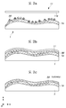
도 2a 내지 도 2c는 평탄화 처리의 개요를 도시하는 도면이다.
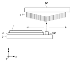
도 3은 평탄화 장치 내의 몰드의 형상을 계측하는 방법을 도시하는 도면이다.
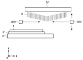
도 4는 평탄화 장치 내의 몰드의 형상을 계측하는 방법을 도시하는 도면이다.
도 5는 평탄화 장치에서의 평탄화 처리를 도시하는 흐름도이다.
Claims (14)
- 몰드의 평면부를 사용하여 기판 상의 지정된 영역 내의 조성물을 평탄화하도록 구성된 평탄화 장치이며,
상기 몰드를 보유지지하도록 구성된 몰드 보유지지 유닛;
상기 몰드 보유지지 유닛에 의해 보유지지되고 상기 기판에 대해 볼록하게 변형된 상기 몰드의 평면부의 형상을 계측하도록 구성된 계측 유닛; 및
상기 계측 유닛의 계측 결과에 기초하여, 상기 몰드의 평면부를 상기 기판 상의 상기 지정된 영역에 정렬시켜 상기 몰드와 상기 조성물을 서로 접촉시키도록 구성된 제어 유닛을 포함하는, 평탄화 장치. - 제1항에 있어서, 상기 계측 유닛은 상기 몰드의 표면과 상기 계측 유닛 사이의 거리를 계측하는, 평탄화 장치.
- 제2항에 있어서, 상기 계측 유닛은 상기 몰드의 표면을 따른 방향으로 복수의 위치에서 상기 거리를 계측하는, 평탄화 장치.
- 제2항에 있어서, 상기 계측 유닛은 상기 기판에 인접한 위치에 배치되는, 평탄화 장치.
- 제1항에 있어서, 상기 계측 유닛은 상기 기판을 보유지지하도록 구성된 기판 보유지지 유닛 상에 제공되는, 평탄화 장치.
- 제1항에 있어서, 상기 계측 유닛은 상기 몰드에 대한 측방향 거리를 계측하기 위한 위치에 배치되는, 평탄화 장치.
- 제6항에 있어서, 상기 계측 유닛은, 상기 기판의 표면에 수직인 방향을 따른 복수의 위치에서, 상기 몰드와 상기 계측 유닛 사이의 거리를 계측하는, 평탄화 장치.
- 제1항에 있어서, 상기 몰드 보유지지 유닛에 의해 보유지지되는 상기 몰드를 상기 기판을 향해 볼록한 형상으로 변형시키도록 구성된 변형 유닛을 더 포함하는, 평탄화 장치.
- 제8항에 있어서,
상기 계측 유닛은, 상기 몰드가 상기 변형 유닛에 의해 볼록하게 변형된 상태에서 상기 계측 유닛과 상기 몰드 사이의 거리를 계측하며,
상기 제어 유닛은, 상기 몰드로부터 상기 기판까지의 거리가 가장 짧은 상기 몰드의 위치를 결정하는, 평탄화 장치. - 제9항에 있어서, 상기 제어 유닛은, 상기 몰드로부터 가장 짧은 거리를 갖는 상기 몰드 상의 상기 위치를 상기 조성물이 평탄화되는 상기 기판의 영역의 중심에 정렬시키는, 평탄화 장치.
- 제1항에 있어서, 상기 몰드는, 상기 몰드가 상기 기판에 대해 볼록한 형상으로 변형된 상태에서 상기 기판 상의 상기 조성물에 접촉되는, 평탄화 장치.
- 제1항에 있어서, 상기 조성물은 상기 기판의 전체 표면에 공급되며 평탄화되는, 평탄화 장치.
- 몰드의 평면부를 사용하여 기판 상의 지정된 영역 내의 조성물을 평탄화하는 평탄화 방법이며,
몰드 보유지지 유닛에 의해 보유지지된 상기 몰드의 평면부의 형상을 계측하는 단계로서, 상기 몰드는 상기 기판에 대해 볼록하게 변형되는, 단계;
상기 계측의 결과에 기초하여, 상기 몰드의 평면부를 상기 기판 상의 상기 지정된 영역에 정렬시키는 단계; 및
상기 기판 상의 상기 지정된 영역 내의 상기 조성물과 상기 몰드를 서로 접촉시키는 단계를 포함하는, 평탄화 방법. - 물품 제조 방법이며,
제13항에 따른 평탄화 방법을 사용하여 기판 상의 조성물을 평탄화하는 단계;
상기 평탄화된 조성물을 위에 포함하는 기판을 처리하는 단계; 및
상기 처리된 기판으로부터 물품을 제조하는 단계를 포함하는, 물품 제조 방법.
Applications Claiming Priority (2)
| Application Number | Priority Date | Filing Date | Title |
|---|---|---|---|
| JP2018171936A JP7150535B2 (ja) | 2018-09-13 | 2018-09-13 | 平坦化装置、平坦化方法及び物品の製造方法 |
| JPJP-P-2018-171936 | 2018-09-13 |
Publications (2)
| Publication Number | Publication Date |
|---|---|
| KR20200031037A true KR20200031037A (ko) | 2020-03-23 |
| KR102571412B1 KR102571412B1 (ko) | 2023-08-28 |
Family
ID=69773955
Family Applications (1)
| Application Number | Title | Priority Date | Filing Date |
|---|---|---|---|
| KR1020190107886A Active KR102571412B1 (ko) | 2018-09-13 | 2019-09-02 | 평탄화 장치, 평탄화 방법 및 물품 제조 방법 |
Country Status (3)
| Country | Link |
|---|---|
| US (1) | US11163231B2 (ko) |
| JP (1) | JP7150535B2 (ko) |
| KR (1) | KR102571412B1 (ko) |
Cited By (1)
| Publication number | Priority date | Publication date | Assignee | Title |
|---|---|---|---|---|
| KR20220049930A (ko) * | 2020-10-15 | 2022-04-22 | (주)휴넷플러스 | 유체 가압을 이용한 반도체 집적소자의 평탄화 방법 |
Families Citing this family (2)
| Publication number | Priority date | Publication date | Assignee | Title |
|---|---|---|---|---|
| JP7418127B2 (ja) * | 2020-03-24 | 2024-01-19 | キヤノン株式会社 | 平坦化装置、平坦化方法及び物品の製造方法 |
| US11752519B2 (en) | 2020-06-19 | 2023-09-12 | Canon Kabushiki Kaisha | Planarization method and photocurable composition |
Citations (6)
| Publication number | Priority date | Publication date | Assignee | Title |
|---|---|---|---|---|
| JPS6363838B2 (ko) * | 1980-03-10 | 1988-12-08 | ||
| KR20130125307A (ko) * | 2012-05-08 | 2013-11-18 | 캐논 가부시끼가이샤 | 임프린트 장치 및 물품 제조 방법 |
| KR101538203B1 (ko) * | 2011-08-11 | 2015-07-20 | 캐논 가부시끼가이샤 | 임프린트 장치 및 물품 제조 방법 |
| US20160349634A1 (en) * | 2015-05-29 | 2016-12-01 | Canon Kabushiki Kaisha | Mold, method and apparatus of imprinting, and method for producing product |
| JP2017174904A (ja) * | 2016-03-22 | 2017-09-28 | キヤノン株式会社 | インプリント装置、インプリント装置の動作方法および物品製造方法 |
| KR20170121707A (ko) * | 2016-04-25 | 2017-11-02 | 캐논 가부시끼가이샤 | 임프린트 장치, 임프린트 방법, 및 물품의 제조 방법 |
Family Cites Families (14)
| Publication number | Priority date | Publication date | Assignee | Title |
|---|---|---|---|---|
| JP2007234733A (ja) | 2006-02-28 | 2007-09-13 | Kawamura Seisakusho:Kk | 転写印刷装置およびそれを用いて印刷した転写印刷製品 |
| WO2009151560A2 (en) * | 2008-06-09 | 2009-12-17 | Board Of Regents, The University Of Texas System | Adaptive nanotopography sculpting |
| NL2003192A1 (nl) | 2008-07-30 | 2010-02-02 | Asml Netherlands Bv | Alignment of collector device in lithographic apparatus. |
| JP5669466B2 (ja) * | 2010-07-12 | 2015-02-12 | キヤノン株式会社 | 保持装置、インプリント装置及び物品の製造方法 |
| JP5930622B2 (ja) | 2010-10-08 | 2016-06-08 | キヤノン株式会社 | インプリント装置、及び、物品の製造方法 |
| JP5935453B2 (ja) * | 2012-03-30 | 2016-06-15 | 大日本印刷株式会社 | 基板の製造方法、および、ナノインプリントリソグラフィ用テンプレートの製造方法 |
| JP6039917B2 (ja) * | 2012-05-22 | 2016-12-07 | キヤノン株式会社 | インプリント装置、インプリント方法及び物品の製造方法 |
| JP6363838B2 (ja) | 2014-01-08 | 2018-07-25 | キヤノン株式会社 | インプリント装置、インプリント方法及び物品の製造方法 |
| JP6472189B2 (ja) * | 2014-08-14 | 2019-02-20 | キヤノン株式会社 | インプリント装置、インプリント方法及び物品の製造方法 |
| JP6478635B2 (ja) | 2015-01-05 | 2019-03-06 | キヤノン株式会社 | インプリント装置、インプリント方法及び物品の製造方法 |
| JP6942491B2 (ja) * | 2016-03-15 | 2021-09-29 | キヤノン株式会社 | インプリント装置、および物品の製造方法 |
| US10035296B2 (en) * | 2016-10-13 | 2018-07-31 | Canon Kabushiki Kaisha | Methods for controlling spread of imprint material |
| JP2019186347A (ja) * | 2018-04-06 | 2019-10-24 | キヤノン株式会社 | 加工装置、インプリント装置、平坦化装置、および加工方法 |
| JP7134725B2 (ja) * | 2018-06-11 | 2022-09-12 | キヤノン株式会社 | 型を用いて基板上の組成物を成形する成形装置、および物品の製造方法 |
-
2018
- 2018-09-13 JP JP2018171936A patent/JP7150535B2/ja active Active
-
2019
- 2019-09-02 KR KR1020190107886A patent/KR102571412B1/ko active Active
- 2019-09-05 US US16/561,838 patent/US11163231B2/en active Active
Patent Citations (6)
| Publication number | Priority date | Publication date | Assignee | Title |
|---|---|---|---|---|
| JPS6363838B2 (ko) * | 1980-03-10 | 1988-12-08 | ||
| KR101538203B1 (ko) * | 2011-08-11 | 2015-07-20 | 캐논 가부시끼가이샤 | 임프린트 장치 및 물품 제조 방법 |
| KR20130125307A (ko) * | 2012-05-08 | 2013-11-18 | 캐논 가부시끼가이샤 | 임프린트 장치 및 물품 제조 방법 |
| US20160349634A1 (en) * | 2015-05-29 | 2016-12-01 | Canon Kabushiki Kaisha | Mold, method and apparatus of imprinting, and method for producing product |
| JP2017174904A (ja) * | 2016-03-22 | 2017-09-28 | キヤノン株式会社 | インプリント装置、インプリント装置の動作方法および物品製造方法 |
| KR20170121707A (ko) * | 2016-04-25 | 2017-11-02 | 캐논 가부시끼가이샤 | 임프린트 장치, 임프린트 방법, 및 물품의 제조 방법 |
Cited By (1)
| Publication number | Priority date | Publication date | Assignee | Title |
|---|---|---|---|---|
| KR20220049930A (ko) * | 2020-10-15 | 2022-04-22 | (주)휴넷플러스 | 유체 가압을 이용한 반도체 집적소자의 평탄화 방법 |
Also Published As
| Publication number | Publication date |
|---|---|
| KR102571412B1 (ko) | 2023-08-28 |
| US20200089108A1 (en) | 2020-03-19 |
| US11163231B2 (en) | 2021-11-02 |
| JP7150535B2 (ja) | 2022-10-11 |
| JP2020043315A (ja) | 2020-03-19 |
Similar Documents
| Publication | Publication Date | Title |
|---|---|---|
| KR20100035111A (ko) | 임프린트 장치 및 물품 제조 방법 | |
| US12491666B2 (en) | Forming apparatus, forming method, and article manufacturing method | |
| KR102571412B1 (ko) | 평탄화 장치, 평탄화 방법 및 물품 제조 방법 | |
| KR20220029413A (ko) | 성형 장치, 성형 방법, 및 템플릿 | |
| US11231648B2 (en) | Imprint device, imprint method, and method for manufacturing article | |
| US11915948B2 (en) | Flattening apparatus, article manufacturing method, flattening method, and imprinting apparatus | |
| JP7218114B2 (ja) | 平坦化装置、平坦化方法及び物品の製造方法 | |
| JP7237519B2 (ja) | 型を用いて基板上の組成物を成形する成形装置、成形方法、および物品の製造方法 | |
| JP7263152B2 (ja) | 成形装置、成形装置を用いた物品製造方法 | |
| TWI870632B (zh) | 平面化設備、平面化方法及物品製造方法 | |
| JP7071231B2 (ja) | 平坦化装置、平坦化方法、物品製造方法及び液滴配置パターンデータの作成方法 | |
| KR102955706B1 (ko) | 형성 장치, 형성 방법 및 물품 제조 방법 | |
| JP7446934B2 (ja) | 型、平坦化装置、平坦化方法及び物品の製造方法 | |
| US12409558B2 (en) | Conveyance apparatus, substrate processing apparatus, conveyance method, and article manufacturing method | |
| JP7851189B2 (ja) | 成形装置、成形方法及び物品の製造方法 | |
| US20260108909A1 (en) | Planarization method, planarization system, and article manufacturing method | |
| JP7195789B2 (ja) | 平坦化装置、及び物品の製造方法 | |
| KR20250099658A (ko) | 성형 장치, 성형 방법 및 물품 제조 방법 | |
| KR20250028210A (ko) | 평탄화 방법 및 물품 제조 방법 | |
| JP2025098718A (ja) | 成形装置、成形方法、および物品製造方法 | |
| JP2025038354A (ja) | 成形装置、成形方法、および物品の製造方法。 |
Legal Events
| Date | Code | Title | Description |
|---|---|---|---|
| PA0109 | Patent application |
St.27 status event code: A-0-1-A10-A12-nap-PA0109 |
|
| PG1501 | Laying open of application |
St.27 status event code: A-1-1-Q10-Q12-nap-PG1501 |
|
| PA0201 | Request for examination |
St.27 status event code: A-1-2-D10-D11-exm-PA0201 |
|
| D13-X000 | Search requested |
St.27 status event code: A-1-2-D10-D13-srh-X000 |
|
| D14-X000 | Search report completed |
St.27 status event code: A-1-2-D10-D14-srh-X000 |
|
| E902 | Notification of reason for refusal | ||
| PE0902 | Notice of grounds for rejection |
St.27 status event code: A-1-2-D10-D21-exm-PE0902 |
|
| P11-X000 | Amendment of application requested |
St.27 status event code: A-2-2-P10-P11-nap-X000 |
|
| P13-X000 | Application amended |
St.27 status event code: A-2-2-P10-P13-nap-X000 |
|
| E701 | Decision to grant or registration of patent right | ||
| PE0701 | Decision of registration |
St.27 status event code: A-1-2-D10-D22-exm-PE0701 |
|
| GRNT | Written decision to grant | ||
| PR0701 | Registration of establishment |
St.27 status event code: A-2-4-F10-F11-exm-PR0701 |
|
| PR1002 | Payment of registration fee |
St.27 status event code: A-2-2-U10-U11-oth-PR1002 Fee payment year number: 1 |
|
| PG1601 | Publication of registration |
St.27 status event code: A-4-4-Q10-Q13-nap-PG1601 |
|
| P22-X000 | Classification modified |
St.27 status event code: A-4-4-P10-P22-nap-X000 |
|
| P22-X000 | Classification modified |
St.27 status event code: A-4-4-P10-P22-nap-X000 |