KR20200032202A - Stacked light sensor assembly with pixel level interconnects - Google Patents
Stacked light sensor assembly with pixel level interconnects Download PDFInfo
- Publication number
- KR20200032202A KR20200032202A KR1020207005992A KR20207005992A KR20200032202A KR 20200032202 A KR20200032202 A KR 20200032202A KR 1020207005992 A KR1020207005992 A KR 1020207005992A KR 20207005992 A KR20207005992 A KR 20207005992A KR 20200032202 A KR20200032202 A KR 20200032202A
- Authority
- KR
- South Korea
- Prior art keywords
- substrate
- photodiode
- diffusion well
- signal
- charge
- Prior art date
- Legal status (The legal status is an assumption and is not a legal conclusion. Google has not performed a legal analysis and makes no representation as to the accuracy of the status listed.)
- Ceased
Links
Images


Classifications
-
- H01L27/14643—
-
- H—ELECTRICITY
- H10—SEMICONDUCTOR DEVICES; ELECTRIC SOLID-STATE DEVICES NOT OTHERWISE PROVIDED FOR
- H10F—INORGANIC SEMICONDUCTOR DEVICES SENSITIVE TO INFRARED RADIATION, LIGHT, ELECTROMAGNETIC RADIATION OF SHORTER WAVELENGTH OR CORPUSCULAR RADIATION
- H10F39/00—Integrated devices, or assemblies of multiple devices, comprising at least one element covered by group H10F30/00, e.g. radiation detectors comprising photodiode arrays
- H10F39/10—Integrated devices
- H10F39/12—Image sensors
- H10F39/18—Complementary metal-oxide-semiconductor [CMOS] image sensors; Photodiode array image sensors
-
- H01L27/14603—
-
- H01L27/14612—
-
- H01L27/14634—
-
- H01L27/14636—
-
- H01L31/10—
-
- H—ELECTRICITY
- H04—ELECTRIC COMMUNICATION TECHNIQUE
- H04N—PICTORIAL COMMUNICATION, e.g. TELEVISION
- H04N25/00—Circuitry of solid-state image sensors [SSIS]; Control thereof
-
- H—ELECTRICITY
- H10—SEMICONDUCTOR DEVICES; ELECTRIC SOLID-STATE DEVICES NOT OTHERWISE PROVIDED FOR
- H10F—INORGANIC SEMICONDUCTOR DEVICES SENSITIVE TO INFRARED RADIATION, LIGHT, ELECTROMAGNETIC RADIATION OF SHORTER WAVELENGTH OR CORPUSCULAR RADIATION
- H10F30/00—Individual radiation-sensitive semiconductor devices in which radiation controls the flow of current through the devices, e.g. photodetectors
- H10F30/20—Individual radiation-sensitive semiconductor devices in which radiation controls the flow of current through the devices, e.g. photodetectors the devices having potential barriers, e.g. phototransistors
-
- H—ELECTRICITY
- H10—SEMICONDUCTOR DEVICES; ELECTRIC SOLID-STATE DEVICES NOT OTHERWISE PROVIDED FOR
- H10F—INORGANIC SEMICONDUCTOR DEVICES SENSITIVE TO INFRARED RADIATION, LIGHT, ELECTROMAGNETIC RADIATION OF SHORTER WAVELENGTH OR CORPUSCULAR RADIATION
- H10F39/00—Integrated devices, or assemblies of multiple devices, comprising at least one element covered by group H10F30/00, e.g. radiation detectors comprising photodiode arrays
- H10F39/10—Integrated devices
- H10F39/12—Image sensors
- H10F39/199—Back-illuminated image sensors
-
- H—ELECTRICITY
- H10—SEMICONDUCTOR DEVICES; ELECTRIC SOLID-STATE DEVICES NOT OTHERWISE PROVIDED FOR
- H10F—INORGANIC SEMICONDUCTOR DEVICES SENSITIVE TO INFRARED RADIATION, LIGHT, ELECTROMAGNETIC RADIATION OF SHORTER WAVELENGTH OR CORPUSCULAR RADIATION
- H10F39/00—Integrated devices, or assemblies of multiple devices, comprising at least one element covered by group H10F30/00, e.g. radiation detectors comprising photodiode arrays
- H10F39/80—Constructional details of image sensors
- H10F39/802—Geometry or disposition of elements in pixels, e.g. address-lines or gate electrodes
-
- H—ELECTRICITY
- H10—SEMICONDUCTOR DEVICES; ELECTRIC SOLID-STATE DEVICES NOT OTHERWISE PROVIDED FOR
- H10F—INORGANIC SEMICONDUCTOR DEVICES SENSITIVE TO INFRARED RADIATION, LIGHT, ELECTROMAGNETIC RADIATION OF SHORTER WAVELENGTH OR CORPUSCULAR RADIATION
- H10F39/00—Integrated devices, or assemblies of multiple devices, comprising at least one element covered by group H10F30/00, e.g. radiation detectors comprising photodiode arrays
- H10F39/80—Constructional details of image sensors
- H10F39/803—Pixels having integrated switching, control, storage or amplification elements
- H10F39/8037—Pixels having integrated switching, control, storage or amplification elements the integrated elements comprising a transistor
-
- H—ELECTRICITY
- H10—SEMICONDUCTOR DEVICES; ELECTRIC SOLID-STATE DEVICES NOT OTHERWISE PROVIDED FOR
- H10F—INORGANIC SEMICONDUCTOR DEVICES SENSITIVE TO INFRARED RADIATION, LIGHT, ELECTROMAGNETIC RADIATION OF SHORTER WAVELENGTH OR CORPUSCULAR RADIATION
- H10F39/00—Integrated devices, or assemblies of multiple devices, comprising at least one element covered by group H10F30/00, e.g. radiation detectors comprising photodiode arrays
- H10F39/80—Constructional details of image sensors
- H10F39/809—Constructional details of image sensors of hybrid image sensors
-
- H—ELECTRICITY
- H10—SEMICONDUCTOR DEVICES; ELECTRIC SOLID-STATE DEVICES NOT OTHERWISE PROVIDED FOR
- H10F—INORGANIC SEMICONDUCTOR DEVICES SENSITIVE TO INFRARED RADIATION, LIGHT, ELECTROMAGNETIC RADIATION OF SHORTER WAVELENGTH OR CORPUSCULAR RADIATION
- H10F39/00—Integrated devices, or assemblies of multiple devices, comprising at least one element covered by group H10F30/00, e.g. radiation detectors comprising photodiode arrays
- H10F39/80—Constructional details of image sensors
- H10F39/811—Interconnections
Landscapes
- Engineering & Computer Science (AREA)
- Multimedia (AREA)
- Signal Processing (AREA)
- Solid State Image Pick-Up Elements (AREA)
- Transforming Light Signals Into Electric Signals (AREA)
- Light Receiving Elements (AREA)
Abstract
실시예들은 2개의 기판들이 수직으로 적층되는 적층된 광 센서 어셈블리에 관한 것이다. 2개의 기판들은 신호를 제 1 기판에서의 포토다이오드로부터 제 2 기판 상의 회로에 제공하기 위해 픽셀 레벨에서 상호연결부들을 통해 연결된다. 제 2 기판 상의 회로는 제 1 기판에서 통상적으로 수행된 동작들을 수행한다. 제 1 및 제 2 기판들을 적층함으로써, 광 센서 어셈블리는 광 센서 어셈블리의 포토다이오드 충전율을 증가시키거나 적어도 유지하면서 더 소형으로 만들어질 수 있다.Embodiments relate to a stacked optical sensor assembly in which two substrates are stacked vertically. The two substrates are connected through interconnects at the pixel level to provide a signal from the photodiode in the first substrate to circuitry on the second substrate. Circuitry on the second substrate performs the operations normally performed on the first substrate. By stacking the first and second substrates, the optical sensor assembly can be made smaller while increasing or at least maintaining the photodiode filling rate of the optical sensor assembly.

Description
본 발명은 일반적으로, 광학 센서들에 관한 것이고, 특히 머신 비전(machine vision)을 위한 후면 조도 광학 센서들에 관한 것이다.The present invention relates generally to optical sensors, and in particular to back-illuminated optical sensors for machine vision.
광학 센서들은 광을 전자 신호로 변환하는 전자 검출기들이다. 사진학에서, 셔터는 광이 결정된 시간 기간 동안 통과하는 것을 허용하여, 장면의 이미지를 캡쳐하기 위해 광학 센서들을 광에 노출시키는 디바이스이다. 롤링 셔터는 정지 사진 또는 비디오의 각각의 프레임이 장면에 걸쳐 가로 또는 세로 방향으로 빠르게 스캔함으로써 캡쳐되는 이미지 캡쳐 방법이다. 즉, 모든 픽셀은 동시에 캡쳐되지 않고; 상이한 행들로부터의 픽셀들은 상이한 시간들에서 캡쳐된다. 롤링 셔터는 주로 휴대폰 센서들에서 사용된다. 머신 비전은 반대로, 모든 픽셀이 동시에 캡쳐되는 글로벌 셔터를 사용한다.Optical sensors are electronic detectors that convert light into electronic signals. In photography, a shutter is a device that allows light to pass through for a determined period of time, exposing optical sensors to light to capture an image of the scene. Rolling shutter is an image capture method in which each frame of a still picture or video is captured by quickly scanning in a horizontal or vertical direction across the scene. That is, not all pixels are captured at the same time; Pixels from different rows are captured at different times. Rolling shutters are mainly used in cell phone sensors. Machine vision, on the contrary, uses a global shutter where all pixels are captured simultaneously.
대부분의 광학 센서들은 후면 조도를 사용한다. 후면 조사 센서는 캡쳐된 광량을 증가시켜 낮은 광 성능을 개선하기 위해 특정 배열의 이미징 요소들을 사용하는 하나의 유형의 디지털 광학 센서이다. 전면에 렌즈가 있으며 후면에 광검출기들이 있는, 전통적인 전면 조도 디지털 카메라는 인간 눈과 유사하게 구성된다. 센서의 이 방향은 디지털 카메라 센서의 능동 매트릭스, 개별적인 픽처 요소들의 매트릭스를 그것의 전면에 배치하고 제조를 단순화한다. 매트릭스 및 그것의 배선은 그러나, 광의 일부를 반사하여 캡쳐될 이용가능한 신호를 감소시킨다. 후면 조사 센서는 동일한 요소들을 포함하지만, 제조 동안 실리콘 웨이퍼를 뒤집고 그 다음, 그것의 뒷면을 얇게 함으로써 광음극 층(photocathode layer) 뒤에 배선을 배열하여 광이 배선층을 통과하지 않고 광음극 층에 닿을 수 있게 하고, 그에 의해 입력 광자가 캡쳐되는 가능성을 개선한다.Most optical sensors use back illumination. The back-illumination sensor is a type of digital optical sensor that uses a specific array of imaging elements to improve the low light performance by increasing the amount of light captured. A traditional front-illuminated digital camera with a lens on the front and photodetectors on the back is constructed similarly to the human eye. This orientation of the sensor places the active matrix of the digital camera sensor, a matrix of individual picture elements in front of it and simplifies manufacturing. The matrix and its wiring, however, reflect some of the light, reducing the available signal to be captured. The back-illumination sensor contains the same elements, but by placing the wiring behind the photocathode layer by turning the silicon wafer over and then thinning its back during manufacturing, the light can reach the photocathode layer without passing through the wiring layer. And thereby improve the possibility that the input photon is captured.
그러나, 종래의 후면 조사 센서들과 연관된 문제점들이 존재한다. 저장장치가 광에 노출되고, 이는 더 많은 누출을 야기한다. 또한, 포토다이오드 충전율(fill factor), 또는 총 픽셀 영역에 대한 픽셀의 감광 영역의 비는 낮다. 더 많은 픽셀 영역이 포토컬렉션을 위해 사용되기 때문에 큰 충전율이 이상적이고, 이는 신호 대 잡음 비(SNR) 및 동적 범위를 동시에 개선한다. 이미지 센서의 동적 범위는 얼마나 넓은 다양한 조명을 센서가 정확하게 캡쳐할 수 있는지를 측정한다. 이미지 센서의 동적 범위가 넓을수록, 낮은 광 조건들 하에서 더 많은 상세들이 보여질 수 있고, 따라서 이미징 시스템의 용도가 더욱 다양해진다. 이미지 센서의 SNR은 신호와 그것의 연관된 잡음 사이의 비를 측정한다. 낮은 SNR을 갖는 이미지 센서는 캡쳐된 이미지에 나타나는 많은 양의 잡음을 가질 것이다. 높은 SNR을 갖는 이미지 센서는 낮은 광 조건들에서 사용될 수 있다. 기존의 후면 조사 센서들과 연관된 문제점들로 인해, 개선된 포토 어셈블리가 바람직할 것이다.However, there are problems associated with conventional backside illumination sensors. The storage device is exposed to light, which causes more leakage. In addition, the photodiode fill factor, or ratio of the photosensitive area of the pixel to the total pixel area, is low. A large fill factor is ideal because more pixel areas are used for photo collection, which simultaneously improves the signal-to-noise ratio (SNR) and dynamic range. The dynamic range of the image sensor measures how wide a variety of lights the sensor can accurately capture. The wider the dynamic range of the image sensor, the more details can be seen under low light conditions, thus the more versatile the use of the imaging system. The SNR of the image sensor measures the ratio between the signal and its associated noise. An image sensor with a low SNR will have a large amount of noise appearing in the captured image. Image sensors with high SNR can be used in low light conditions. Due to the problems associated with existing back illumination sensors, an improved photo assembly would be desirable.
실시예들은 적층된 기판들을 갖는 광 센서의 픽셀 및 적층된 기판들에서 회로들을 연결하는 픽셀 레벨 상호연결부에 관한 것이다. 픽셀은 제 1 기판의 일부, 제 1 기판으로부터의 신호를 프로세싱하기 위한 회로를 가지는 제 2 기판의 일부; 및 픽셀 레벨 상호연결부를 포함할 수 있다. 제 1 기판의 부분은 광을 검출하기 위한 포토다이오드, 및 포토다이오드로부터의 광전하를 저장하기 위해 포토다이오드와 연관된 확산 우물(diffusion well)을 포함한다. 확산 우물에 저장된 전하량은 포토다이오드에 입사되는 광의 지속기간 및 세기에 의존한다. 픽셀 레벨 상호연결부는 신호를 제 2 확산 우물로부터 회로에 반송하기 위해 제 1 기판의 제 2 확산 우물을 제 2 기판의 회로에 연결한다.Embodiments relate to a pixel of an optical sensor having stacked substrates and a pixel level interconnect connecting circuits in the stacked substrates. The pixel includes a portion of the first substrate, a portion of the second substrate having circuitry for processing signals from the first substrate; And a pixel level interconnect. The portion of the first substrate includes a photodiode for detecting light, and a diffusion well associated with the photodiode to store photocharges from the photodiode. The amount of charge stored in the diffusion well depends on the duration and intensity of the light incident on the photodiode. The pixel level interconnect connects the second diffusion well of the first substrate to the circuit of the second substrate to convey a signal from the second diffusion well to the circuit.
본 발명에 따른 실시예들은 광 센서의 픽셀, 방법, 저장 매체, 시스템 및 컴퓨터 프로그램 제품에 관한 첨부된 청구항들에 특히 개시되고, 하나의 청구항 카테고리 예로서, 픽셀에서 언급된 임의의 특징은 또 다른 청구항 카테고리, 예로서, 방법에서 또한 청구될 수 있다. 다시, 첨부된 청구항들에서의 종속성들 또는 참조들은 단지 공식적인 이유들을 위해 선택된다. 그러나, 임의의 이전의 청구항들(특히, 다수의 종속성들)에 대해 다시 의도적인 참조로부터 발생하는 임의의 요지가 또한, 청구될 수 있어서, 청구항들 및 그들의 특징들의 임의의 조합이 개시되고 첨부된 도면들에서 선택된 종속성들에 관계없이 청구될 수 있게 한다. 청구될 수 있는 요지는 첨부된 청구항들에 제시된 바와 같은 특징들의 조합들 뿐만 아니라, 청구항들에서의 특징들의 임의의 다른 조합을 포함하고, 청구항들에서 언급된 각각의 특징은 청구항들에서의 임의의 다른 특징 또는 다른 특징들의 조합과 조합될 수 있다. 또한, 본 명세서에서 설명되거나 묘사된 실시예들 및 특징들 중 임의의 실시예 및 특징은 별개의 청구항에서 및/또는 본 명세서에서 설명되거나 묘사된 임의의 실시예 또는 특징과 또는 첨부된 청구항들의 특징들 중 임의의 특징과의 임의의 조합으로 청구될 수 있다.Embodiments according to the invention are particularly disclosed in the appended claims relating to pixels, methods, storage media, systems and computer program products of optical sensors, and as one claim category example, any feature referred to in a pixel is another It may also be claimed in the claims category, eg, in the method. Again, dependencies or references in the appended claims are chosen for official reasons only. However, any subject matter arising from an intentional reference again to any previous claims (in particular, multiple dependencies) may also be claimed so that any combination of the claims and their features is disclosed and appended drawings. Allows to be claimed regardless of the dependencies selected in the field. The subject matter that may be claimed includes combinations of features as set forth in the appended claims, as well as any other combination of features in the claims, and each feature referred to in the claims is any other in the claims. It can be combined with a feature or a combination of other features. In addition, any of the embodiments and features described or depicted herein may be defined in the separate claims and / or any embodiment or features described or depicted herein or the features of the appended claims. It can be claimed in any combination with any of the features.
본 발명에 따른 일 실시예에서, 광 센서의 픽셀은: 제 1 기판의 일부로서, 광을 검출하기 위한 포토다이오드, 및 포토다이오드로부터의 전하를 저장하기 위해 포토다이오드와 연관된 확산 우물을 포함하고, 확산 우물에 저장된 전하량은 포토다이오드에 입사되는 광의 지속기간 및 세기에 의존하는, 상기 제 1 기판의 일부; 제 1 기판으로부터의 신호를 프로세싱하기 위한 회로를 가지는 제 2 기판의 일부; 및 신호를 확산 우물로부터 회로에 반송하기 위해 제 1 기판의 제 2 우물을 제 2 기판의 회로에 연결하는 픽셀 레벨 상호연결부를 포함한다.In one embodiment according to the present invention, the pixel of the light sensor comprises: as part of a first substrate, a photodiode for detecting light, and a diffusion well associated with the photodiode for storing charge from the photodiode, The amount of charge stored in the diffusion well depends on the duration and intensity of light incident on the photodiode, a portion of the first substrate; A portion of a second substrate having circuitry for processing signals from the first substrate; And a pixel level interconnect connecting the second well of the first substrate to the circuit of the second substrate for conveying the signal from the diffusion well to the circuit.
제 1 기판은: 픽셀의 비 노출 시간 동안 턴 온(turn on)된 제 1 트랜지스터; 및 포토다이오드에 저장된 광전하를 우물로 전송하기 위해 턴 온된 제 2 트랜지스터를 더 포함할 수 있다.The first substrate includes: a first transistor turned on during a non-exposure time of the pixel; And a second transistor turned on to transmit the photocharge stored in the photodiode to the well.
제 1 기판은 P 도핑될 수 있고, 확산 우물 및 다른 확산 우물은 N 도핑될 수 있다.The first substrate may be P doped, and the diffusion well and other diffusion wells may be N doped.
제 1 기판은 제 2 기판에 대면하는 확산 우물 및 포토다이오드로 형성된 전면을 가질 수 있다.The first substrate may have a diffusion well facing the second substrate and a front surface formed of a photodiode.
제 2 기판은 회로로 형성된 전면 및 제 2 기판의 대향 측에서의 후면을 가질 수 있고, 전면은 제 1 기판에 대면한다.The second substrate may have a front side formed of a circuit and a rear side on the opposite side of the second substrate, the front side facing the first substrate.
신호는 포토다이오드로부터 확산 우물로 전송된 전하량에 의존하는 전압 신호일 수 있다.The signal may be a voltage signal depending on the amount of charge transferred from the photodiode to the diffusion well.
프로세싱은 샘플링 및 아날로그 디지털 변환 중 적어도 하나를 포함할 수 있다.Processing may include at least one of sampling and analog to digital conversion.
본 발명에 따른 또 다른 실시예에서, 광 센서를 동작시키기 위한 방법은: 제 1 기판의 포토다이오드에 의해 광을 검출하는 단계; 제 1 기판의 확산 우물에 의해 포토다이오드로부터의 전하를 저장하는 단계로서, 전하는 포토다이오드에 입사되는 광의 지속기간 및 세기에 의존하는, 상기 전하를 제 1 기판에 저장하는 단계; 확산 우물에 저장된 전하를 표현하는 신호를 제 1 기판에서 생성하는 단계; 제 1 기판의 확산 우물을 제 2 기판의 회로에 연결하는 픽셀 레벨 상호연결부에 의해 신호를 제 1 기판으로부터 제 2 기판으로 전송하는 단계; 및 제 2 기판의 회로에 의해 신호를 프로세싱하는 단계를 포함한다.In another embodiment according to the invention, a method for operating an optical sensor comprises: detecting light by a photodiode of a first substrate; Storing the charge from the photodiode by the diffusion well of the first substrate, the charge being dependent on the duration and intensity of light incident on the photodiode, storing the charge on the first substrate; Generating a signal representing a charge stored in the diffusion well on the first substrate; Transmitting a signal from the first substrate to the second substrate by a pixel level interconnect that connects the diffusion well of the first substrate to the circuit of the second substrate; And processing the signal by circuitry on the second substrate.
방법은: 픽셀의 비 노출 시간 동안 제 1 트랜지스터를 턴 온하는 단계; 제 1 트랜지스터가 턴 온하는 것에 응답하여 전하를 또 다른 확산 우물로부터 포토다이오드로 전송하는 단계; 및 포토다이오드에 저장된 전하를 확산 우물로 전송하기 위해 제 2 트랜지스터를 턴 온하는 단계를 더 포함할 수 있다.The method comprises: turning on the first transistor during the non-exposed time of the pixel; Transferring charge from another diffusion well to the photodiode in response to the first transistor turning on; And turning on the second transistor to transfer the charge stored in the photodiode to the diffusion well.
제 1 기판은 P 도핑될 수 있고, 확산 우물 및 다른 확산 우물은 N 도핑될 수 있다.The first substrate may be P doped, and the diffusion well and other diffusion wells may be N doped.
제 1 기판은 제 2 기판에 대면하는 확산 우물 및 포토다이오드로 형성된 전면을 가질 수 있다.The first substrate may have a diffusion well facing the second substrate and a front surface formed of a photodiode.
제 2 기판은 회로로 형성된 전면 및 제 2 기판의 대향 측에서의 후면을 가질 수 있고, 전면은 제 1 기판에 대면한다.The second substrate may have a front side formed of a circuit and a rear side on the opposite side of the second substrate, the front side facing the first substrate.
신호는 포토다이오드로부터 확산 우물로 전송된 전하량에 의존하는 전압 신호일 수 있다.The signal may be a voltage signal depending on the amount of charge transferred from the photodiode to the diffusion well.
프로세싱은 샘플링 및 아날로그 디지털 변환 중 적어도 하나를 포함할 수 있다.Processing may include at least one of sampling and analog to digital conversion.
본 발명의 또 다른 실시예에서, 하나 이상의 컴퓨터 판독가능한 비일시적 저장 매체들은 본 발명에 따른 시스템 또는 상기 언급된 실시예들 중 임의의 실시예에서 수행하도록 실행될 때 동작가능한 소프트웨어를 구현한다.In another embodiment of the present invention, one or more computer-readable non-transitory storage media implement software operable when executed to perform in a system according to the present invention or any of the above-mentioned embodiments.
본 발명의 또 다른 실시예에서, 컴퓨터 구현 방법은 본 발명에 따른 시스템 또는 상기 언급된 실시예들 중 임의의 실시예를 사용한다.In another embodiment of the present invention, a computer-implemented method uses a system according to the present invention or any of the above-mentioned embodiments.
본 발명의 또 다른 실시예에서, 바람직하게 컴퓨터 판독가능한 비일시적 저장 매체들을 포함하는 컴퓨터 프로그램 제품은 본 발명에 따른 시스템 또는 상기 언급된 실시예들 중 임의의 실시예에서 사용된다.In another embodiment of the invention, a computer program product, preferably comprising computer-readable non-transitory storage media, is used in a system according to the invention or in any of the above-mentioned embodiments.
상기 발명에 따른 시스템에서 수행하도록 실행될 때 동작가능한 소프트웨어를 구현하는 하나 이상의 컴퓨터 판독가능한 비일시적 저장 매체들.One or more computer-readable non-transitory storage media implementing software operable when executed to perform in a system according to the invention.
상기 발명에 따른 시스템이 사용되는 컴퓨터 구현 방법.A computer-implemented method in which the system according to the invention is used.
상기 발명에 따른 저장 매체가 사용되는 컴퓨터 구현 방법.A computer-implemented method in which a storage medium according to the invention is used.
도 1은 하나의 실시예에 따른, 전자 디바이스를 도시하는 고 레벨 블록도.
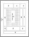
도 2는 하나의 실시예에 따른, 센서 아키텍처를 도시하는 도면.
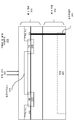
도 3은 하나의 실시예에 따른, 적층된 포토 어셈블리를 도시하는 단면도.
도 4는 적층된 광 센서 어셈블리의 프로세스 흐름을 도시하는 도면.1 is a high level block diagram illustrating an electronic device, according to one embodiment.
2 illustrates a sensor architecture, according to one embodiment.
3 is a cross-sectional view showing a stacked photo assembly, according to one embodiment.
4 shows the process flow of a stacked optical sensor assembly.
도면들은 단지 예시의 목적들을 위해 다양한 실시예를 묘사한다. 당업자는 다음 논의로부터 본 명세서에 도시된 구조들 및 방법들의 대안적인 실시예들이 본 명세서에 설명된 원리들을 벗어나지 않고 채용될 수 있음을 용이하게 인식할 것이다.The drawings depict various embodiments for purposes of illustration only. Those skilled in the art will readily appreciate from the following discussion that alternative embodiments of the structures and methods depicted herein can be employed without departing from the principles described herein.
이제 바람직한 실시예에 대한 참조가 상세하게 행해질 것이며, 그 예는 첨부된 도면들에 도시된다. 가능할 때마다, 도면들에 걸쳐 동일하거나 유사한 부분들을 언급하기 위해 동일한 참조 부호들이 사용될 것이다.Reference will now be made in detail to the preferred embodiment, an example of which is shown in the accompanying drawings. Whenever possible, identical reference numerals will be used to refer to the same or similar parts throughout the drawings.
실시예들은 2개의 기판들이 수직으로 적층되는 적층된 광 센서 어셈블리에 관한 것이다. 2개의 기판들은 신호를 제 1 기판에서의 포토다이오드로부터 제 2 기판 상의 회로에 신호를 제공하기 위해 픽셀 레벨에서 상호연결부들을 통해 연결된다. 제 2 기판 상의 회로는 제 1 기판에서 통상적으로 수행된 동작들을 수행한다. 제 1 및 제 2 기판들을 적층함으로써, 광 센서 어셈블리는 광 센서 어셈블리의 포토다이오드 충전율을 증가시키거나 적어도 유지하면서 더 소형으로 만들어질 수 있다.Embodiments relate to a stacked optical sensor assembly in which two substrates are stacked vertically. The two substrates are connected via interconnects at the pixel level to provide a signal from the photodiode in the first substrate to circuitry on the second substrate. Circuitry on the second substrate performs the operations normally performed on the first substrate. By stacking the first and second substrates, the optical sensor assembly can be made smaller while increasing or at least maintaining the photodiode filling rate of the optical sensor assembly.
예시적인 시스템 아키텍처Example system architecture
도 1은 하나의 실시예에 따른, 전자 디바이스를 도시하는 고 레벨 블록도이다. 하나의 실시예에서, 전자 디바이스(100)는 다른 구성요소들 중에서, 상호적으로 결합되는 프로세서(102) 및 광 센서(104)를 포함한다. 전자 디바이스(100)은 메모리 및 다양한 다른 센서들과 같은 도 1에 도시되지 않은 다른 구성요소들을 포함할 수 있다.1 is a high-level block diagram illustrating an electronic device, according to one embodiment. In one embodiment, the
프로세서(102)는 데이터 소스에 대한 동작들을 수행하는 전자 회로이다. 데이터 소스는 센서 데이터(108)를 제공하는 광 센서(104)를 포함할 수 있다. 프로세서(102)는 광 센서(104)로 전송되는 동작 명령들(106)을 생성한다. 프로세서(102)에 의해 수행된 프로세싱은 센서 데이터(108)의 아날로그 디지털 변환을 포함할 수 있고, 이는 전압 아날로그 신호들 또는 전류 아날로그 신호들을 디지털 신호들로 변환한다.
광 센서(104)는 광 세기를 측정하고 광변환을 수행하는 회로이다. 광 세기를 측정하는 것은 포토다이오드에 의해 광을 검출하는 것을 수반할 수 있고 광변환은 포토다이오드에 의해 광을 전압 또는 전류 신호로 변환하는 것을 수반할 수 있다.The optical sensor 104 is a circuit that measures light intensity and performs light conversion. Measuring light intensity can involve detecting light by a photodiode and photoconversion can involve converting light into a voltage or current signal by a photodiode.
도 2는 하나의 실시예에 따른, 광 센서(104)를 도시하는 개략도이다. 광 센서(104)는 다른 구성요소들 중에서, 디지털 블록(202), 글로벌 카운터(203), 행 구동기들 및 글로벌 신호 구동기 모듈(204), MIPI(Mobile Industry Processor Interface)(205), 카운터 버퍼들(206), 디지털 픽셀 어레이(207), 감지 증폭기들(208), 라인 메모리(209), 전력 컨디셔너(power conditioner)(210), 램프 생성 및 버퍼 모듈(211), 및 감지 증폭 바이어싱 모듈(212)을 포함한다.2 is a schematic diagram illustrating an optical sensor 104 according to one embodiment. The optical sensor 104 includes, among other components, a
디지털 블록(202)은 광 센서(104)의 동작과 연관된 디지털 신호들을 프로세싱하는 회로이다. 하나 이상의 실시예들에서, 디지털 블록(202)의 적어도 일부는 회로가 디지털 픽셀 어레이(207)와 별개인 대신에 디지털 픽셀 어레이(207)의 일부로서 제공될 수 있다.The
글로벌 카운터(203)는 캐스케이딩 플립 플롭(cascading flip-flop)들로 구성된 디지털 순차 논리 회로이고, 광 센서(104)의 다양한 구성요소들에 카운터 신호들을 제공한다.The
행 구동기들 및 글로벌 신호 구동기 모듈(204)은 스캔 라인들(도시되지 않음)을 통해 픽셀들의 행들에 신호들을 제공하는 회로이다. 픽셀들의 각각의 행에 제공된 신호는 이미지 신호의 감지 및/또는 픽셀들의 각각의 행에서 재설정 동작들을 나타낸다.The row drivers and global
MTPI(205)는 센서 데이터(108)를 광 센서(104)로부터 프로세서(102)로 송신하기 위한 직렬 인터페이스이다. MIPI 인터페이스는 전형적으로, 직렬 데이터를 반송하는 단일 클록 레인 및 2개의 데이터 레인들(도시되지 않음)을 갖는다. 이들 3개의 레인들은 와이어들의 쌍들에 신호들을 반송하고, 여기서 신호들은 종종 차동이다.
카운터 버퍼들(206)은 글로벌 카운터(203)로부터 카운터 신호들을 수신하고, 감지 및 재설정 동작들을 조정하기 위해 디지털 픽셀 어레이(207)에서 신호들을 픽셀들의 열들로 전송하는 회로이다.Counter buffers 206 are circuits that receive counter signals from
디지털 픽셀 어레이(207)는 복수의 픽셀들을 포함한다. 하나의 실시예에서, 디지털 픽셀 어레이는 행 및 열에 의해 주소지정가능한 2차원들로 배열된다. 각각의 픽셀은 광을 감지하고 입력 광의 세기에 대응하는 신호를 출력하도록 구성된다. 각각의 픽셀은 도 3을 참조하여 하기에 설명된 바와 같은 구성요소들을 포함할 수 있다.The
감지 증폭기들(208)은 디지털 픽셀 어레이(207)로부터 디지털 신호들을 판독하기 위해 사용되는 판독 회로에서의 요소들이다. 감지 증폭기들(208)은 디지털 픽셀 어레이(207)에서 픽셀들에 의해 캡쳐된 광의 세기를 표현하는 비트라인으로부터 저전력 신호들을 감지한다. 감지 증폭기들(208)은 아날로그 디지털 변환기(ADC)를 활용함으로써 디지털 출력 신호를 생성할 수 있다. 하나 이상의 실시예들에서, 감지 증폭기들(208)의 적어도 일부는 디지털 픽셀 어레이(207)에 포함될 수 있다.
라인 메모리(209)는 MIPI(205)를 통해 디지털 값들을 센서 데이터(108)로서 프로세서(102)로 전송하기 전에 감지 증폭기들(208)에 의해 감지되고 디지털 블록(202)에 의해 프로세싱된 바와 같이, 디지털 픽셀 어레이(207)에서 검출된 광 세기의 감지된 디지털 값들을 일시적으로 저장한다.The
전력 컨디셔너(210)는 광 센서(104)의 구성요소들에 전달되는 전력의 품질을 개선하는 회로이다. 전력 컨디셔너(210)는 광 센서(104)의 구성요소들이 적절하게 기능하는 것을 허용하는 일정한 전압을 유지 및 전달할 수 있다. 하나의 실시예에서, 전력 컨디셔너(210)는 정현 AC 파형을 평활화하는 AC 전력 컨디셔너이다. 대안적인 실시예들에서, 전력 컨디셔너(210)는 전력 라인 컨디셔너에 연결된 구성요소들의 요건들에 기초하여 전력을 취하고 그것을 수정하는 전력 라인 컨디셔너이다.The
램프 생성기 및 버퍼 모듈(211)은 램프 생성기 및 버퍼들을 포함한다. 램프 생성기는 그것의 전압을 특정 값으로 증가시키는 함수 생성기이다. 램프 생성기는 부하를 변경할 때 충격들을 회피하기 위해 사용될 수 있다. 버퍼들은 램프 생성기가 부하에 의해 영향을 받는 것을 방지하기 위해 하나의 회로로부터 또 다른 회로로 전기 임피던스 전환을 제공한다.The lamp generator and
감지 증폭 바이어싱 모듈(212)은 감지 증폭기들(208)에 바이어싱 전압 신호를 제공한다. 바이어싱 전압 신호는 DC 정전압과 같은 감지 증폭기들(208)의 적절한 동작 조건들을 확립하는 목적을 위해 미리 정해진 전압이다.The sense amplifying
예시적인 적층된 광 센서 어셈블리Example stacked light sensor assembly
도 3은 하나의 실시예에 따른, 적층된 광 센서 어셈블리(300)를 도시하는 단면도이다. 하나의 실시예에서, 적층된 포토 어셈블리는 제 2 기판(340)에 연결된 제 1 기판(310)을 포함한다. 제 1 기판(310)은 뒤집히고 다른 구성요소들 중에서, 제 1 n+ 확산 우물(312), 포토다이오드(314), 트랜지스터 AB(313), 트랜지스터 TX(316), 및 제 2 n+ 확산 우물(320)을 포함하는 후면 조도(302) 센서일 수 있다.3 is a cross-sectional view illustrating a stacked
트랜지스터 AB(311) 및 트랜지스터 TX(316)의 각각은 활성층, 활성층에 결합된 드레인 전극, 트랜지스터 AB 및 트랜지스터 TX 둘 모두의 소스의 역할을 하는 포토다이오드(314), 활성층 위의 절연층, 및 게이트 전극(도시되지 않음)을 포함한다. 트랜지스터들 AB(311) 및 트랜지스터 TX(316)의 게이트들에서 전압 레벨을 제어함으로써, 트랜지스터들 AB(311) 및 트랜지스터 TX(316)는 턴 온 또는 오프될 수 있다. 이들 트랜지스터들의 게이트들은 디지털 픽셀 어레이(207) 외부의 회로들로부터 신호들을 수신한다.Each of the transistors AB 311 and
제 1 n+ 확산 우물(312)은 제 1 기판(310)에서 형성된 N 도핑된 주입 영역이다. 제 1 n+ 확산 우물(312)은 비 노출 시간들 동안 트랜지스터 AB(313)가 턴 온될 때 포토다이오드(314)로부터 전송되는 광전자들을 수용한다. 이것은 전통적인 필름 카메라에서 폐쇄 셔터 모드와 동등하다. 포토다이오드(314)로부터 n+ 확산 우물(312)로의 광전자들의 전송은 비 노출 시간들이 어떠한 신호도 생성되지 않을 기간들이기 때문에, 포토다이오드(314)에 어떠한 광전자들도 축적되지 않음을 보장한다. n+ 확산 우물(312)은 전형적으로, 양의 전압원 예를 들면, VDD에 연결되고 따라서, 광전자들이 배출된다. 필름 카메라에서 셔터 개방 모드와 동등한 노출 시간 동안, 트랜지스터 AB(313) 및 트랜지스터 TX(316) 둘 모두는 턴 오프되고 광전자들은 초기에 포토다이오드(314) 내부에 저장된다. 노출의 종료 시에, 트랜지스터 TX(316)는 턴 온된다. 결과적으로, 포토다이오드(314)에 저장된 전하는 제 2 n+ 확산 우물(320)로 전송된다.The first n + diffusion well 312 is an N doped implantation region formed in the
포토다이오드(314)는 광을 전류로 변환하는 반도체 디바이스이다. 전류는 광자들이 포토다이오드(314)에서 흡수될 때 생성된다. 포토다이오드(314)는 p-n 접합 또는 PIN 구조일 수 있다. 후면 조도(302)를 통한 광의 세기가 더 높을 때, 포토다이오드(314)에 축적된 전하량은 크다. 유사하게, 후면 조도(302)를 통한 광의 세기가 더 낮을 때, 포토다이오드(314)에 축적된 전하량은 적다.The
상호연결부(350)는 n+ 확산 우물(320)로부터 제 2 기판(340)에서의 회로(342)까지의 픽셀 레벨 직접 상호연결부일 수 있다. 하나의 실시예에서, 상호연결부(350)는 포토다이오드(314)로부터 n+ 확산 우물(320)로 전송된 전하량을 반영하는 전압 신호를 송신한다. 대안적인 실시예들에서, 상호연결부(350)는 포토다이오드(314)로부터 n+ 확산 우물(320)로 전송된 전하량을 반영하는 전류 신호를 송신한다. 상호연결부(350)는 샘플링 및 아날로그 디지털 변환과 같은 또 다른 프로세싱을 위해 전압 신호를 회로(342)에 반송한다. 또 다른 실시예들에서, 적층된 광 센서 어셈블리(300)는 제 2 기판(340)의 회로(342)로부터 제 1 기판(310)으로 신호들을 또한 송신하는 부가적인 상호연결부들을 포함할 수 있다. 예를 들면, 트랜지스터 AB(313) 및 트랜지스터 TX(316)를 제어하기 위한 신호들은 이들 부가적인 상호연결부들을 통해 회로(342)로부터 송신될 수 있다.The
실시예들은 종래의 광 센서들에서 제 1 기판(310)에 제공된 다양한 회로 구성요소들을 제 2 기판(340)으로 이동시키고, 제 2 기판(340)의 회로들을 픽셀 레벨 상호연결부(350)를 통해 제 1 기판(310)에서의 구성요소들에 연결한다. 제 2 기판(340)으로 이동된 다양한 회로 구성요소들은 특히, 스위치들, 증폭기들 및 전류원을 포함할 수 있다. 이러한 방식으로, 제 1 기판(310)에서 구성요소들에 의해 점유된 영역은 유리하게 감소될 수 있고 충전율이 증가될 수 있다.Embodiments move the various circuit components provided in the
적층된 광 센서 어셈블리에서 동작의 예시적인 프로세스Example process of operation in a stacked light sensor assembly
도 4는 적층된 광 센서 어셈블리의 프로세스 흐름을 도시하는 도면이다. 첫째, 비 노출, 또는 셔터 폐쇄 기간 동안 제 1 기판(310)에서 포토다이오드(314)로부터 제 1 n+ 확산 우물(312)로 전하가 전송된다(420). 구체적으로, 트랜지스터 AB(313)는 제 1 n+ 확산 우물(312)과 포토다이오드(314) 사이에 전류 경로를 제공하기 위해 턴 온된다. 둘째, 노출 시간 동안, 셔터가 개방되고, 전하가 포토다이오드(314)에 축적된다.4 is a diagram showing the process flow of the stacked optical sensor assembly. First, charge is transferred (420) from the
노출 시간이 종료된 후에, 포토다이오드(314)에 축적된 전하는 제 2 n+ 확산부(320)로 전송된다(425). 구체적으로, 포토다이오드(314)에서의 전하를 제 2 n+ 확산 우물(320)로 전송하도록 전류 경로를 제공하기 위해 트랜지스터 AB(313)는 턴 오프되고, 트랜지스터 TX(316)는 턴 온된다.After the exposure time ends, the charge accumulated in the
제 2 n+ 우물(320)로 전송된 전하에 기초하여, 신호는 제 1 기판(310)에서 생성된다(430). 신호는 전압 신호 또는 전류 신호일 수 있다.Based on the charge transferred to the second n + well 320, a signal is generated at the first substrate 310 (430). The signal can be a voltage signal or a current signal.
신호는 그 다음, 픽셀 레벨 상호연결부(350)를 통해 제 1 기판(310)으로부터 제 1 기판(310)에 적층된 제 2 기판(340)으로 송신된다(435).The signal is then transmitted from the
제 2 기판(340)에서의 회로(342)는 상호연결부(350)를 통해 송신된 신호를 수신한다(440). 회로(342)는 프로세서(102)로 전송하기 위해 수신된 신호를 프로세싱한다(445).The circuit 342 on the
실시예들의 상기 설명은 예시의 목적을 위해 제공되었고; 그것은 철저한 것으로 의도되지 않거나 특허권들을 개시된 정확한 형태들로 제한하도록 의도되지 않는다. 관련 분야에서의 숙련자들은 상기 개시에 비추어 많은 수정들 및 변형들이 가능하다는 것을 이해할 수 있다.The above description of embodiments has been provided for purposes of illustration; It is not intended to be exhaustive or to limit patent rights to the precise forms disclosed. Those skilled in the art can understand that many modifications and variations are possible in light of the above disclosure.
본 명세서에서 사용된 언어는 원칙적으로, 가독성 및 교육 목적들을 위해 선택되었으며, 그것은 특허권들을 상세하게 설명하거나 제한하기 위해 선택되지 않았을 수 있다. 따라서, 특허권들의 범위는 이 상세한 설명에 의해 제한되는 것이 아니라, 여기에 기초한 출원에 관해 발행되는 임의의 청구항들에 의해 제한되는 것으로 의도된다. 그에 따라, 실시예들의 개시는 특허권들의 범위를 제한하기 위한 것이 아니라 예시적인 것으로 의도되며, 이는 다음의 청구항들에 제시된다.The language used in this specification was, in principle, selected for readability and educational purposes, which may not have been selected to detail or limit patent rights. Accordingly, it is intended that the scope of the patent rights not be limited by this detailed description, but rather by any claims issued with respect to the application based thereon. Accordingly, the disclosure of the embodiments is intended to be illustrative rather than limiting the scope of the patent rights, which are set forth in the following claims.
Claims (28)
제 1 기판의 일부로서,
광을 검출하기 위한 포토다이오드, 및
상기 포토다이오드로부터의 전하를 저장하기 위해 상기 포토다이오드와 연관된 확산 우물(diffusion well)로서, 상기 확산 우물에 저장된 전하량은 상기 포토다이오드에 입사되는 상기 광의 지속기간 및 세기에 의존하는, 상기 확산 우물을 포함하는, 상기 제 1 기판의 일부;
상기 제 1 기판으로부터의 신호를 프로세싱하기 위한 회로를 가지는 제 2 기판의 일부; 및
상기 신호를 상기 확산 우물로부터 상기 회로에 반송하기 위해 상기 제 1 기판의 제 2 우물을 상기 제 2 기판의 회로에 연결하는 픽셀 레벨 상호연결부를 포함하는, 광 센서의 픽셀.For the pixels of the light sensor:
As part of the first substrate,
A photodiode for detecting light, and
A diffusion well associated with the photodiode to store charge from the photodiode, wherein the amount of charge stored in the diffusion well depends on the duration and intensity of the light incident on the photodiode. Included, a portion of the first substrate;
A portion of a second substrate having circuitry for processing signals from the first substrate; And
And a pixel level interconnect connecting the second well of the first substrate to the circuit of the second substrate for conveying the signal from the diffusion well to the circuit.
상기 제 1 기판은:
상기 픽셀의 비 노출 시간 동안 턴 온(turn on)된 제 1 트랜지스터; 및
상기 포토다이오드에 저장된 광전하를 상기 우물로 전송하기 위해 턴 온된 제 2 트랜지스터를 더 포함하는, 광 센서의 픽셀.According to claim 1,
The first substrate is:
A first transistor turned on during the non-exposure time of the pixel; And
And a second transistor turned on to transmit the photocharge stored in the photodiode to the well.
상기 제 1 기판은 P 도핑되고, 상기 확산 우물 및 다른 확산 우물은 N 도핑되는, 광 센서의 픽셀.According to claim 1,
The first substrate is P doped, and the diffusion well and the other diffusion well are N doped, the pixels of the optical sensor.
상기 제 1 기판은 상기 제 2 기판에 대면하는 상기 확산 우물 및 상기 포토다이오드로 형성된 전면을 가지는, 광 센서의 픽셀.According to claim 1,
Wherein the first substrate has a front surface formed of the diffusion well and the photodiode facing the second substrate.
상기 제 2 기판은 상기 회로로 형성된 전면 및 상기 제 2 기판의 대향 측에서의 후면을 가지고, 상기 전면은 상기 제 1 기판에 대면하는, 광 센서의 픽셀.According to claim 1,
The second substrate has a front surface formed of the circuit and a rear surface on the opposite side of the second substrate, the front surface facing the first substrate, the pixel of the optical sensor.
상기 신호는 상기 포토다이오드로부터 상기 확산 우물로 전송된 전하량에 의존하는 전압 신호인, 광 센서의 픽셀.According to claim 1,
The signal is a voltage signal depending on the amount of charge transferred from the photodiode to the diffusion well, the pixel of the optical sensor.
상기 프로세싱은 샘플링 및 아날로그 디지털 변환 중 적어도 하나를 포함하는, 광 센서의 픽셀.According to claim 1,
The processing comprises at least one of sampling and analog to digital conversion, the pixel of the optical sensor.
제 1 기판의 포토다이오드에 의해 광을 검출하는 단계;
상기 제 1 기판의 확산 우물에 의해 상기 포토다이오드로부터의 전하를 저장하는 단계로서, 상기 전하는 상기 포토다이오드에 입사되는 광의 지속기간 및 세기에 의존하는, 상기 저장 단계;
상기 확산 우물에 저장된 전하를 표현하는 신호를 상기 제 1 기판에서 생성하는 단계;
상기 제 1 기판의 확산 우물을 제 2 기판의 회로에 연결하는 픽셀 레벨 상호연결부에 의해 상기 신호를 상기 제 1 기판으로부터 상기 제 2 기판으로 전송하는 단계; 및
상기 제 2 기판에서 상기 회로에 의해 상기 신호를 프로세싱하는 단계를 포함하는, 광 센서를 동작시키기 위한 방법.In the method for operating the optical sensor:
Detecting light by a photodiode of the first substrate;
Storing the charge from the photodiode by the diffusion well of the first substrate, wherein the charge is dependent on the duration and intensity of light incident on the photodiode;
Generating a signal representing the charge stored in the diffusion well on the first substrate;
Transmitting the signal from the first substrate to the second substrate by a pixel level interconnect connecting the diffusion well of the first substrate to the circuit of the second substrate; And
And processing the signal by the circuitry on the second substrate.
상기 픽셀의 비 노출 시간 동안 제 1 트랜지스터를 턴 온하는 단계;
상기 제 1 트랜지스터가 턴 온하는 것에 응답하여 전하를 또 다른 확산 우물로부터 상기 포토다이오드로 전송하는 단계; 및
상기 포토다이오드에 저장된 전하를 상기 확산 우물로 전송하기 위해 제 2 트랜지스터를 턴 온하는 단계를 더 포함하는, 광 센서를 동작시키기 위한 방법.The method of claim 8,
Turning on a first transistor during the non-exposure time of the pixel;
Transferring charge from another diffusion well to the photodiode in response to the first transistor turning on; And
And turning on a second transistor to transfer charge stored in the photodiode to the diffusion well.
상기 제 1 기판은 P 도핑되고, 상기 확산 우물 및 다른 확산 우물은 N 도핑되는, 광 센서를 동작시키기 위한 방법.The method of claim 8,
The first substrate is P-doped, and the diffusion well and the other diffusion well are N-doped.
상기 제 1 기판은 상기 제 2 기판에 대면하는 상기 확산 우물 및 상기 포토다이오드로 형성된 전면을 가지는, 광 센서를 동작시키기 위한 방법.The method of claim 8,
And the first substrate has a front surface formed of the diffusion well and the photodiode facing the second substrate.
상기 제 2 기판은 상기 회로로 형성된 전면 및 상기 제 2 기판의 대향 측에서의 후면을 가지고, 상기 전면은 상기 제 1 기판에 대면하는, 광 센서를 동작시키기 위한 방법.The method of claim 8,
The second substrate has a front surface formed by the circuit and a rear surface on the opposite side of the second substrate, the front surface facing the first substrate, the method for operating the optical sensor.
상기 신호는 상기 포토다이오드로부터 상기 확산 우물로 전송된 전하량에 의존하는 전압 신호인, 광 센서를 동작시키기 위한 방법.The method of claim 8,
The signal is a voltage signal that is dependent on the amount of charge transferred from the photodiode to the diffusion well.
상기 프로세싱은 샘플링 및 아날로그 디지털 변환 중 적어도 하나를 포함하는, 광 센서를 동작시키기 위한 방법.The method of claim 8,
The processing comprises at least one of sampling and analog to digital conversion.
제 1 기판의 일부로서,
광을 검출하기 위한 포토다이오드, 및
상기 포토다이오드로부터의 전하를 저장하기 위해 상기 포토다이오드와 연관된 확산 우물로서, 상기 확산 우물에 저장된 전하량은 상기 포토다이오드에 입사되는 상기 광의 지속기간 및 세기에 의존하는, 상기 확산 우물을 포함하는, 상기 제 1 기판의 일부;
상기 제 1 기판으로부터의 신호를 프로세싱하기 위한 회로를 가지는 제 2 기판의 일부; 및
상기 신호를 상기 확산 우물로부터 상기 회로에 반송하기 위해 상기 제 1 기판의 제 2 우물을 상기 제 2 기판의 회로에 연결하는 픽셀 레벨 상호연결부를 포함하는, 광 센서의 픽셀.For the pixels of the light sensor:
As part of the first substrate,
A photodiode for detecting light, and
A diffusion well associated with the photodiode for storing charge from the photodiode, the amount of charge stored in the diffusion well comprising the diffusion well, depending on the duration and intensity of the light incident on the photodiode A portion of the first substrate;
A portion of a second substrate having circuitry for processing signals from the first substrate; And
And a pixel level interconnect that connects the second well of the first substrate to the circuit of the second substrate to convey the signal from the diffusion well to the circuit.
상기 제 1 기판은:
상기 픽셀의 비 노출 시간 동안 턴 온된 제 1 트랜지스터; 및
상기 포토다이오드에 저장된 광전하를 상기 우물로 전송하기 위해 턴 온된 제 2 트랜지스터를 더 포함하는, 광 센서의 픽셀.The method of claim 15,
The first substrate is:
A first transistor turned on during the non-exposure time of the pixel; And
And a second transistor turned on to transmit the photocharge stored in the photodiode to the well.
상기 제 1 기판은 P 도핑되고, 상기 확산 우물 및 다른 확산 우물은 N 도핑되는, 광 센서의 픽셀.The method of claim 15 or 16,
The first substrate is P doped, and the diffusion well and the other diffusion well are N doped, the pixels of the optical sensor.
상기 제 1 기판은 상기 제 2 기판에 대면하는 상기 확산 우물 및 상기 포토다이오드로 형성된 전면을 가지는, 광 센서의 픽셀.The method according to any one of claims 15 to 17,
Wherein the first substrate has a front surface formed of the diffusion well and the photodiode facing the second substrate.
상기 제 2 기판은 상기 회로로 형성된 전면 및 상기 제 2 기판의 대향 측에서의 후면을 가지고, 상기 전면은 상기 제 1 기판에 대면하는, 광 센서의 픽셀.The method according to any one of claims 15 to 18,
The second substrate has a front surface formed of the circuit and a rear surface on the opposite side of the second substrate, the front surface facing the first substrate, the pixel of the optical sensor.
상기 신호는 상기 포토다이오드로부터 상기 확산 우물로 전송된 전하량에 의존하는 전압 신호인, 광 센서의 픽셀.The method according to any one of claims 15 to 19,
The signal is a voltage signal depending on the amount of charge transferred from the photodiode to the diffusion well, the pixel of the optical sensor.
상기 프로세싱은 샘플링 및 아날로그 디지털 변환 중 적어도 하나를 포함하는, 광 센서의 픽셀.The method according to any one of claims 15 to 20,
The processing comprises at least one of sampling and analog to digital conversion, the pixel of the optical sensor.
제 1 기판의 포토다이오드에 의해 광을 검출하는 단계;
상기 제 1 기판의 확산 우물에 의해 상기 포토다이오드로부터의 전하를 저장하는 단계로서, 상기 전하는 상기 포토다이오드에 입사되는 광의 지속기간 및 세기에 의존하는, 상기 저장 단계;
상기 확산 우물에 저장된 전하를 표현하는 신호를 상기 제 1 기판에서 생성하는 단계;
상기 제 1 기판의 확산 우물을 제 2 기판의 회로에 연결하는 픽셀 레벨 상호연결부에 의해 상기 신호를 상기 제 1 기판으로부터 상기 제 2 기판으로 전송하는 단계; 및
상기 제 2 기판의 상기 회로에 의해 상기 신호를 프로세싱하는 단계를 포함하는, 광 센서를 동작시키기 위한 방법.In the method for operating the optical sensor:
Detecting light by a photodiode of the first substrate;
Storing the charge from the photodiode by the diffusion well of the first substrate, wherein the charge is dependent on the duration and intensity of light incident on the photodiode;
Generating a signal representing the charge stored in the diffusion well on the first substrate;
Transmitting the signal from the first substrate to the second substrate by a pixel level interconnect connecting the diffusion well of the first substrate to the circuit of the second substrate; And
And processing the signal by the circuitry of the second substrate.
상기 픽셀의 비 노출 시간 동안 제 1 트랜지스터를 턴 온하는 단계;
상기 제 1 트랜지스터가 턴 온하는 것에 응답하여 전하를 또 다른 확산 우물로부터 상기 포토다이오드로 전송하는 단계; 및
상기 포토다이오드에 저장된 전하를 상기 확산 우물로 전송하기 위해 제 2 트랜지스터를 턴 온하는 단계를 더 포함하는, 광 센서를 동작시키기 위한 방법.The method of claim 22,
Turning on a first transistor during the non-exposure time of the pixel;
Transferring charge from another diffusion well to the photodiode in response to the first transistor turning on; And
And turning on a second transistor to transfer charge stored in the photodiode to the diffusion well.
상기 제 1 기판은 P 도핑되고, 상기 확산 우물 및 다른 확산 우물은 N 도핑되는, 광 센서를 동작시키기 위한 방법.The method of claim 22 or 23,
The first substrate is P-doped, and the diffusion well and the other diffusion well are N-doped.
상기 제 1 기판은 상기 제 2 기판에 대면하는 상기 확산 우물 및 상기 포토다이오드로 형성된 전면을 가지는, 광 센서를 동작시키기 위한 방법.The method according to any one of claims 22 to 24,
And the first substrate has a front surface formed of the diffusion well and the photodiode facing the second substrate.
상기 제 2 기판은 상기 회로로 형성된 전면 및 상기 제 2 기판의 대향 측에서의 후면을 가지고, 상기 전면은 상기 제 1 기판에 대면하는, 광 센서를 동작시키기 위한 방법.The method according to any one of claims 22 to 25,
The second substrate has a front surface formed of the circuit and a rear surface on the opposite side of the second substrate, the front surface facing the first substrate, a method for operating an optical sensor.
상기 신호는 상기 포토다이오드로부터 상기 확산 우물로 전송된 전하량에 의존하는 전압 신호인, 광 센서를 동작시키기 위한 방법.The method according to any one of claims 22 to 26,
The signal is a voltage signal that is dependent on the amount of charge transferred from the photodiode to the diffusion well.
상기 프로세싱은 샘플링 및 아날로그 디지털 변환 중 적어도 하나를 포함하는, 광 센서를 동작시키기 위한 방법.The method according to any one of claims 22 to 27,
The processing comprises at least one of sampling and analog to digital conversion.
Applications Claiming Priority (5)
| Application Number | Priority Date | Filing Date | Title |
|---|---|---|---|
| US201762546476P | 2017-08-16 | 2017-08-16 | |
| US62/546,476 | 2017-08-16 | ||
| US15/801,216 | 2017-11-01 | ||
| US15/801,216 US10825854B2 (en) | 2017-08-16 | 2017-11-01 | Stacked photo sensor assembly with pixel level interconnect |
| PCT/US2018/045673 WO2019036240A1 (en) | 2017-08-16 | 2018-08-07 | Stacked photo sensor assembly with pixel level interconnect |
Publications (1)
| Publication Number | Publication Date |
|---|---|
| KR20200032202A true KR20200032202A (en) | 2020-03-25 |
Family
ID=65361604
Family Applications (1)
| Application Number | Title | Priority Date | Filing Date |
|---|---|---|---|
| KR1020207005992A Ceased KR20200032202A (en) | 2017-08-16 | 2018-08-07 | Stacked light sensor assembly with pixel level interconnects |
Country Status (6)
| Country | Link |
|---|---|
| US (1) | US10825854B2 (en) |
| JP (1) | JP2020532098A (en) |
| KR (1) | KR20200032202A (en) |
| CN (1) | CN111033745A (en) |
| TW (1) | TW201911547A (en) |
| WO (1) | WO2019036240A1 (en) |
Cited By (1)
| Publication number | Priority date | Publication date | Assignee | Title |
|---|---|---|---|---|
| WO2022119170A1 (en) * | 2020-12-04 | 2022-06-09 | (주)딥인사이트 | Optical device having monolithic architecture and method for manufacturing same |
Families Citing this family (28)
| Publication number | Priority date | Publication date | Assignee | Title |
|---|---|---|---|---|
| US10917589B2 (en) | 2017-06-26 | 2021-02-09 | Facebook Technologies, Llc | Digital pixel with extended dynamic range |
| US10419701B2 (en) | 2017-06-26 | 2019-09-17 | Facebook Technologies, Llc | Digital pixel image sensor |
| US10686996B2 (en) | 2017-06-26 | 2020-06-16 | Facebook Technologies, Llc | Digital pixel with extended dynamic range |
| US10608101B2 (en) * | 2017-08-16 | 2020-03-31 | Facebook Technologies, Llc | Detection circuit for photo sensor with stacked substrates |
| US10825854B2 (en) * | 2017-08-16 | 2020-11-03 | Facebook Technologies, Llc | Stacked photo sensor assembly with pixel level interconnect |
| US10598546B2 (en) | 2017-08-17 | 2020-03-24 | Facebook Technologies, Llc | Detecting high intensity light in photo sensor |
| US11393867B2 (en) | 2017-12-06 | 2022-07-19 | Facebook Technologies, Llc | Multi-photodiode pixel cell |
| US10969273B2 (en) | 2018-03-19 | 2021-04-06 | Facebook Technologies, Llc | Analog-to-digital converter having programmable quantization resolution |
| US11004881B2 (en) | 2018-04-03 | 2021-05-11 | Facebook Technologies, Llc | Global shutter image sensor |
| US11233085B2 (en) | 2018-05-09 | 2022-01-25 | Facebook Technologies, Llc | Multi-photo pixel cell having vertical gate structure |
| US11089241B2 (en) | 2018-06-11 | 2021-08-10 | Facebook Technologies, Llc | Pixel cell with multiple photodiodes |
| US11906353B2 (en) | 2018-06-11 | 2024-02-20 | Meta Platforms Technologies, Llc | Digital pixel with extended dynamic range |
| US10903260B2 (en) | 2018-06-11 | 2021-01-26 | Facebook Technologies, Llc | Multi-photodiode pixel cell |
| US11089210B2 (en) | 2018-06-11 | 2021-08-10 | Facebook Technologies, Llc | Configurable image sensor |
| US11463636B2 (en) | 2018-06-27 | 2022-10-04 | Facebook Technologies, Llc | Pixel sensor having multiple photodiodes |
| US10897586B2 (en) | 2018-06-28 | 2021-01-19 | Facebook Technologies, Llc | Global shutter image sensor |
| US10931884B2 (en) | 2018-08-20 | 2021-02-23 | Facebook Technologies, Llc | Pixel sensor having adaptive exposure time |
| US11956413B2 (en) | 2018-08-27 | 2024-04-09 | Meta Platforms Technologies, Llc | Pixel sensor having multiple photodiodes and shared comparator |
| US11595602B2 (en) | 2018-11-05 | 2023-02-28 | Meta Platforms Technologies, Llc | Image sensor post processing |
| US11102430B2 (en) | 2018-12-10 | 2021-08-24 | Facebook Technologies, Llc | Pixel sensor having multiple photodiodes |
| US11218660B1 (en) | 2019-03-26 | 2022-01-04 | Facebook Technologies, Llc | Pixel sensor having shared readout structure |
| US11943561B2 (en) | 2019-06-13 | 2024-03-26 | Meta Platforms Technologies, Llc | Non-linear quantization at pixel sensor |
| US11936998B1 (en) | 2019-10-17 | 2024-03-19 | Meta Platforms Technologies, Llc | Digital pixel sensor having extended dynamic range |
| US11902685B1 (en) | 2020-04-28 | 2024-02-13 | Meta Platforms Technologies, Llc | Pixel sensor having hierarchical memory |
| US11910114B2 (en) | 2020-07-17 | 2024-02-20 | Meta Platforms Technologies, Llc | Multi-mode image sensor |
| US11956560B2 (en) | 2020-10-09 | 2024-04-09 | Meta Platforms Technologies, Llc | Digital pixel sensor having reduced quantization operation |
| US12022218B2 (en) | 2020-12-29 | 2024-06-25 | Meta Platforms Technologies, Llc | Digital image sensor using a single-input comparator based quantizer |
| US12477854B2 (en) | 2023-03-08 | 2025-11-18 | Semiconductor Components Industries, Llc | Image sensor signal path routing |
Family Cites Families (64)
| Publication number | Priority date | Publication date | Assignee | Title |
|---|---|---|---|---|
| JP2953297B2 (en) | 1994-03-30 | 1999-09-27 | 日本電気株式会社 | Light receiving element and driving method thereof |
| US6486504B1 (en) | 1999-10-26 | 2002-11-26 | Eastman Kodak Company | CMOS image sensor with extended dynamic range |
| US20030049925A1 (en) * | 2001-09-10 | 2003-03-13 | Layman Paul Arthur | High-density inter-die interconnect structure |
| CN1234234C (en) * | 2002-09-30 | 2005-12-28 | 松下电器产业株式会社 | Solid-state photographic device and equipment using the photographic device |
| US7280143B2 (en) | 2003-04-14 | 2007-10-09 | Micron Technology, Inc. | CMOS image sensor with active reset and 4-transistor pixels |
| US6885331B2 (en) | 2003-09-15 | 2005-04-26 | Micron Technology, Inc. | Ramp generation with capacitors |
| JP4317115B2 (en) | 2004-04-12 | 2009-08-19 | 国立大学法人東北大学 | Solid-state imaging device, optical sensor, and operation method of solid-state imaging device |
| JP4349232B2 (en) * | 2004-07-30 | 2009-10-21 | ソニー株式会社 | Semiconductor module and MOS solid-state imaging device |
| US8144227B2 (en) * | 2004-09-02 | 2012-03-27 | Sony Corporation | Image pickup device and image pickup result outputting method |
| TW201101476A (en) * | 2005-06-02 | 2011-01-01 | Sony Corp | Semiconductor image sensor module and method of manufacturing the same |
| KR100775058B1 (en) | 2005-09-29 | 2007-11-08 | 삼성전자주식회사 | An image processing system including a pixel, an image sensor using the same, and the image sensor |
| US7326903B2 (en) | 2006-06-29 | 2008-02-05 | Noble Peak Vision Corp. | Mixed analog and digital pixel for high dynamic range readout |
| US7361989B1 (en) * | 2006-09-26 | 2008-04-22 | International Business Machines Corporation | Stacked imager package |
| KR101154389B1 (en) * | 2007-09-21 | 2012-06-15 | 삼성전자주식회사 | Pixel Cell, Image Sensor Adopting The Pixel Cell, and Image Processing System Including The Image Sensor |
| EP2104234B1 (en) | 2008-03-21 | 2011-08-31 | STMicroelectronics Limited | Analog-to-digital conversion in image sensors |
| US7795650B2 (en) | 2008-12-09 | 2010-09-14 | Teledyne Scientific & Imaging Llc | Method and apparatus for backside illuminated image sensors using capacitively coupled readout integrated circuits |
| JP4941490B2 (en) * | 2009-03-24 | 2012-05-30 | ソニー株式会社 | Solid-state imaging device and electronic apparatus |
| EP2234387B8 (en) | 2009-03-24 | 2012-05-23 | Sony Corporation | Solid-state imaging device, driving method of solid-state imaging device, and electronic apparatus |
| JP4987917B2 (en) * | 2009-08-19 | 2012-08-01 | 株式会社東芝 | Method for manufacturing solid-state imaging device |
| US8569807B2 (en) * | 2009-09-01 | 2013-10-29 | Taiwan Semiconductor Manufacturing Company, Ltd. | Backside illuminated image sensor having capacitor on pixel region |
| JP5330520B2 (en) | 2009-09-11 | 2013-10-30 | パナソニック株式会社 | Analog / digital converter, image sensor system, camera device |
| JP5489705B2 (en) * | 2009-12-26 | 2014-05-14 | キヤノン株式会社 | Solid-state imaging device and imaging system |
| JP5500007B2 (en) * | 2010-09-03 | 2014-05-21 | ソニー株式会社 | Solid-state imaging device and camera system |
| TWI462265B (en) | 2010-11-30 | 2014-11-21 | 財團法人工業技術研究院 | Image capture device |
| US8847136B2 (en) * | 2011-01-02 | 2014-09-30 | Pixim, Inc. | Conversion gain modulation using charge sharing pixel |
| KR101241704B1 (en) | 2011-04-14 | 2013-03-19 | 엘지이노텍 주식회사 | Pixel, pixel array, image sensor including the same and method for operating the image sensor |
| US8575531B2 (en) | 2011-04-26 | 2013-11-05 | Aptina Imaging Corporation | Image sensor array for back side illumination with global shutter using a junction gate photodiode |
| JP5791571B2 (en) * | 2011-08-02 | 2015-10-07 | キヤノン株式会社 | Imaging device and imaging apparatus |
| JP5868065B2 (en) | 2011-08-05 | 2016-02-24 | キヤノン株式会社 | Imaging device |
| JP5901186B2 (en) | 2011-09-05 | 2016-04-06 | キヤノン株式会社 | Solid-state imaging device and driving method thereof |
| US20130056809A1 (en) | 2011-09-07 | 2013-03-07 | Duli Mao | Image Sensor with Reduced Noiseby Blocking Nitridation Over Selected Areas |
| US8461660B2 (en) * | 2011-09-30 | 2013-06-11 | Omnivision Technologies, Inc. | CMOS image sensor with reset shield line |
| JP5963421B2 (en) | 2011-11-17 | 2016-08-03 | オリンパス株式会社 | Solid-state imaging device and imaging device |
| KR20130062188A (en) | 2011-12-02 | 2013-06-12 | 삼성전자주식회사 | Image sensor, and image processing device including the same |
| TW201340708A (en) | 2012-03-19 | 2013-10-01 | 新力股份有限公司 | Solid-state imaging device and electronic device |
| US8957358B2 (en) | 2012-04-27 | 2015-02-17 | Taiwan Semiconductor Manufacturing Company, Ltd. | CMOS image sensor chips with stacked scheme and methods for forming the same |
| US8779346B2 (en) | 2012-05-14 | 2014-07-15 | BAE Systems Imaging Solutions Inc. | Digital pixel sensor with reduced noise |
| JP6071315B2 (en) * | 2012-08-08 | 2017-02-01 | オリンパス株式会社 | Solid-state imaging device and imaging device |
| US9343497B2 (en) * | 2012-09-20 | 2016-05-17 | Semiconductor Components Industries, Llc | Imagers with stacked integrated circuit dies |
| US9094612B2 (en) * | 2012-09-25 | 2015-07-28 | Semiconductor Components Industries, Llc | Back side illuminated global shutter image sensors with back side charge storage |
| US9478579B2 (en) * | 2012-10-16 | 2016-10-25 | Omnivision Technologies, Inc. | Stacked chip image sensor with light-sensitive circuit elements on the bottom chip |
| JPWO2014080625A1 (en) * | 2012-11-22 | 2017-01-05 | 株式会社ニコン | Imaging device and imaging unit |
| US9153616B2 (en) | 2012-12-26 | 2015-10-06 | Olympus Corporation | Solid-state imaging device and imaging device with circuit elements distributed on multiple substrates, method of controlling solid-state imaging device, and imaging device with circuit elements distributed on multiple substrates |
| US8773562B1 (en) | 2013-01-31 | 2014-07-08 | Apple Inc. | Vertically stacked image sensor |
| JP2014236183A (en) | 2013-06-05 | 2014-12-15 | 株式会社東芝 | Image sensor device and method of manufacturing the same |
| JP6188451B2 (en) | 2013-06-27 | 2017-08-30 | オリンパス株式会社 | Analog-digital converter and solid-state imaging device |
| US10043843B2 (en) | 2013-10-01 | 2018-08-07 | Forza Silicon Corporation | Stacked photodiodes for extended dynamic range and low light color discrimination |
| KR102210539B1 (en) | 2013-12-26 | 2021-02-01 | 삼성전자주식회사 | correlated double sampling circuit, analog-to digital converter and image sensor including the same |
| EP2924979B1 (en) | 2014-03-25 | 2023-01-18 | IMEC vzw | Improvements in or relating to imaging sensors |
| TWI656631B (en) | 2014-03-28 | 2019-04-11 | 日商半導體能源研究所股份有限公司 | Imaging device |
| US9432597B2 (en) | 2014-07-25 | 2016-08-30 | Rambus Inc. | Low-noise, high dynamic-range image sensor |
| US9344658B2 (en) * | 2014-07-31 | 2016-05-17 | Omnivision Technologies, Inc. | Negative biased substrate for pixels in stacked image sensors |
| US9332200B1 (en) | 2014-12-05 | 2016-05-03 | Qualcomm Incorporated | Pixel readout architecture for full well capacity extension |
| US9819882B2 (en) | 2015-06-05 | 2017-11-14 | Caeleste Cvba | Global shutter high dynamic range sensor |
| KR102460175B1 (en) * | 2015-08-21 | 2022-10-28 | 삼성전자주식회사 | Shared pixel and image sensor including the same |
| US10014333B2 (en) | 2015-08-26 | 2018-07-03 | Semiconductor Components Industries, Llc | Back-side illuminated pixels with interconnect layers |
| US9654712B2 (en) * | 2015-10-07 | 2017-05-16 | Semiconductor Components Industries, Llc | Pixels with a global shutter and high dynamic range |
| KR102433575B1 (en) | 2015-10-12 | 2022-08-19 | 삼성전자주식회사 | Image sensor |
| US9991306B2 (en) | 2015-12-10 | 2018-06-05 | Semiconductor Components Industries, Llc | Hybrid bonded image sensor and method of operating such image sensor |
| US10419701B2 (en) | 2017-06-26 | 2019-09-17 | Facebook Technologies, Llc | Digital pixel image sensor |
| US10750097B2 (en) * | 2017-08-14 | 2020-08-18 | Facebooke Technologies, Llc | Varying exposure time of pixels in photo sensor using motion prediction |
| US10608101B2 (en) * | 2017-08-16 | 2020-03-31 | Facebook Technologies, Llc | Detection circuit for photo sensor with stacked substrates |
| US10825854B2 (en) * | 2017-08-16 | 2020-11-03 | Facebook Technologies, Llc | Stacked photo sensor assembly with pixel level interconnect |
| US10598546B2 (en) * | 2017-08-17 | 2020-03-24 | Facebook Technologies, Llc | Detecting high intensity light in photo sensor |
-
2017
- 2017-11-01 US US15/801,216 patent/US10825854B2/en active Active
-
2018
- 2018-08-07 WO PCT/US2018/045673 patent/WO2019036240A1/en not_active Ceased
- 2018-08-07 KR KR1020207005992A patent/KR20200032202A/en not_active Ceased
- 2018-08-07 CN CN201880052917.2A patent/CN111033745A/en active Pending
- 2018-08-07 JP JP2020505189A patent/JP2020532098A/en active Pending
- 2018-08-15 TW TW107128468A patent/TW201911547A/en unknown
Cited By (1)
| Publication number | Priority date | Publication date | Assignee | Title |
|---|---|---|---|---|
| WO2022119170A1 (en) * | 2020-12-04 | 2022-06-09 | (주)딥인사이트 | Optical device having monolithic architecture and method for manufacturing same |
Also Published As
| Publication number | Publication date |
|---|---|
| WO2019036240A1 (en) | 2019-02-21 |
| CN111033745A (en) | 2020-04-17 |
| US20190057995A1 (en) | 2019-02-21 |
| US10825854B2 (en) | 2020-11-03 |
| JP2020532098A (en) | 2020-11-05 |
| TW201911547A (en) | 2019-03-16 |
Similar Documents
| Publication | Publication Date | Title |
|---|---|---|
| KR20200032202A (en) | Stacked light sensor assembly with pixel level interconnects | |
| US10608101B2 (en) | Detection circuit for photo sensor with stacked substrates | |
| US11927475B2 (en) | Detecting high intensity light in photo sensor | |
| US10750097B2 (en) | Varying exposure time of pixels in photo sensor using motion prediction | |
| US8085321B2 (en) | Method and apparatus for providing a rolling double reset timing for global storage in image sensors | |
| US9247170B2 (en) | Triple conversion gain image sensor pixels | |
| US9854184B2 (en) | Imaging pixels with a fully depleted charge transfer path | |
| KR20190069557A (en) | Image sensor pixel with overflow capability | |
| US20090237541A1 (en) | Method and apparatus providing reduced metal routing in imagers | |
| CN206302500U (en) | Imaging pixels | |
| EP3445037B1 (en) | Varying exposure time of pixels in photo sensor using motion prediction | |
| CN110557583B (en) | Image sensor, method of operating image sensor, and imaging system | |
| US8031247B2 (en) | Method and apparatus providing an imager with a shared power supply and readout line for pixels | |
| EP3445039B1 (en) | Detection circuit for photo sensor with stacked substrates | |
| EP3445038A1 (en) | Stacked photo sensor assembly with pixel level interconnect | |
| EP3445040B1 (en) | Detecting high intensity light in photo sensor |
Legal Events
| Date | Code | Title | Description |
|---|---|---|---|
| PA0105 | International application |
Patent event date: 20200228 Patent event code: PA01051R01D Comment text: International Patent Application |
|
| PG1501 | Laying open of application | ||
| PA0201 | Request for examination |
Patent event code: PA02012R01D Patent event date: 20210607 Comment text: Request for Examination of Application |
|
| E902 | Notification of reason for refusal | ||
| PE0902 | Notice of grounds for rejection |
Comment text: Notification of reason for refusal Patent event date: 20221007 Patent event code: PE09021S01D |
|
| E601 | Decision to refuse application | ||
| PE0601 | Decision on rejection of patent |
Patent event date: 20230223 Comment text: Decision to Refuse Application Patent event code: PE06012S01D Patent event date: 20221007 Comment text: Notification of reason for refusal Patent event code: PE06011S01I |