KR20200032247A - 메모리 어레이에 결합된 디코드 회로 - Google Patents
메모리 어레이에 결합된 디코드 회로 Download PDFInfo
- Publication number
- KR20200032247A KR20200032247A KR1020207007516A KR20207007516A KR20200032247A KR 20200032247 A KR20200032247 A KR 20200032247A KR 1020207007516 A KR1020207007516 A KR 1020207007516A KR 20207007516 A KR20207007516 A KR 20207007516A KR 20200032247 A KR20200032247 A KR 20200032247A
- Authority
- KR
- South Korea
- Prior art keywords
- access line
- coupled
- memory
- memory array
- region
- Prior art date
- Legal status (The legal status is an assumption and is not a legal conclusion. Google has not performed a legal analysis and makes no representation as to the accuracy of the status listed.)
- Granted
Links
Images


Classifications
-
- G—PHYSICS
- G11—INFORMATION STORAGE
- G11C—STATIC STORES
- G11C13/00—Digital stores characterised by the use of storage elements not covered by groups G11C11/00, G11C23/00, or G11C25/00
- G11C13/0002—Digital stores characterised by the use of storage elements not covered by groups G11C11/00, G11C23/00, or G11C25/00 using resistive RAM [RRAM] elements
- G11C13/0021—Auxiliary circuits
- G11C13/0023—Address circuits or decoders
-
- G—PHYSICS
- G11—INFORMATION STORAGE
- G11C—STATIC STORES
- G11C8/00—Arrangements for selecting an address in a digital store
- G11C8/10—Decoders
-
- G—PHYSICS
- G11—INFORMATION STORAGE
- G11C—STATIC STORES
- G11C13/00—Digital stores characterised by the use of storage elements not covered by groups G11C11/00, G11C23/00, or G11C25/00
- G11C13/0002—Digital stores characterised by the use of storage elements not covered by groups G11C11/00, G11C23/00, or G11C25/00 using resistive RAM [RRAM] elements
- G11C13/0021—Auxiliary circuits
- G11C13/0023—Address circuits or decoders
- G11C13/0026—Bit-line or column circuits
-
- G—PHYSICS
- G11—INFORMATION STORAGE
- G11C—STATIC STORES
- G11C13/00—Digital stores characterised by the use of storage elements not covered by groups G11C11/00, G11C23/00, or G11C25/00
- G11C13/0002—Digital stores characterised by the use of storage elements not covered by groups G11C11/00, G11C23/00, or G11C25/00 using resistive RAM [RRAM] elements
- G11C13/0021—Auxiliary circuits
- G11C13/0023—Address circuits or decoders
- G11C13/0028—Word-line or row circuits
-
- G—PHYSICS
- G11—INFORMATION STORAGE
- G11C—STATIC STORES
- G11C13/00—Digital stores characterised by the use of storage elements not covered by groups G11C11/00, G11C23/00, or G11C25/00
- G11C13/0002—Digital stores characterised by the use of storage elements not covered by groups G11C11/00, G11C23/00, or G11C25/00 using resistive RAM [RRAM] elements
- G11C13/0021—Auxiliary circuits
- G11C13/003—Cell access
-
- G—PHYSICS
- G11—INFORMATION STORAGE
- G11C—STATIC STORES
- G11C5/00—Details of stores covered by group G11C11/00
- G11C5/02—Disposition of storage elements, e.g. in the form of a matrix array
- G11C5/025—Geometric lay-out considerations of storage- and peripheral-blocks in a semiconductor storage device
-
- G—PHYSICS
- G11—INFORMATION STORAGE
- G11C—STATIC STORES
- G11C5/00—Details of stores covered by group G11C11/00
- G11C5/06—Arrangements for interconnecting storage elements electrically, e.g. by wiring
- G11C5/063—Voltage and signal distribution in integrated semi-conductor memory access lines, e.g. word-line, bit-line, cross-over resistance, propagation delay
-
- G—PHYSICS
- G11—INFORMATION STORAGE
- G11C—STATIC STORES
- G11C7/00—Arrangements for writing information into, or reading information out from, a digital store
- G11C7/10—Input/output [I/O] data interface arrangements, e.g. I/O data control circuits, I/O data buffers
- G11C7/1015—Read-write modes for single port memories, i.e. having either a random port or a serial port
- G11C7/1039—Read-write modes for single port memories, i.e. having either a random port or a serial port using pipelining techniques, i.e. using latches between functional memory parts, e.g. row/column decoders, I/O buffers, sense amplifiers
-
- G—PHYSICS
- G11—INFORMATION STORAGE
- G11C—STATIC STORES
- G11C7/00—Arrangements for writing information into, or reading information out from, a digital store
- G11C7/18—Bit line organisation; Bit line lay-out
-
- G—PHYSICS
- G11—INFORMATION STORAGE
- G11C—STATIC STORES
- G11C8/00—Arrangements for selecting an address in a digital store
- G11C8/14—Word line organisation; Word line lay-out
-
- G—PHYSICS
- G11—INFORMATION STORAGE
- G11C—STATIC STORES
- G11C8/00—Arrangements for selecting an address in a digital store
- G11C8/16—Multiple access memory array, e.g. addressing one storage element via at least two independent addressing line groups
-
- G—PHYSICS
- G11—INFORMATION STORAGE
- G11C—STATIC STORES
- G11C2213/00—Indexing scheme relating to G11C13/00 for features not covered by this group
- G11C2213/70—Resistive array aspects
- G11C2213/71—Three dimensional array
-
- H—ELECTRICITY
- H10—SEMICONDUCTOR DEVICES; ELECTRIC SOLID-STATE DEVICES NOT OTHERWISE PROVIDED FOR
- H10D—INORGANIC ELECTRIC SEMICONDUCTOR DEVICES
- H10D88/00—Three-dimensional [3D] integrated devices
Landscapes
- Engineering & Computer Science (AREA)
- Microelectronics & Electronic Packaging (AREA)
- Semiconductor Memories (AREA)
Abstract
Description
도 2a는 본 개시의 다수의 실시예에 따라 메모리 어레이의 일부의 예의 3차원 등각도이다.
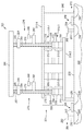
도 2b는 본 개시의 다수의 실시예에 따라 장치의 일부의 단면도이다.
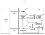
도 3은 본 개시의 다수의 실시예에 따라 장치의 또 다른 예의 블록도이다.
Claims (25)
- 장치에 있어서,
제1 영역 내의 메모리 어레이; 및
반도체로부터 분리된 제2 영역 내의 디코드 회로를 포함하고;
상기 디코드 회로는 상기 메모리 어레이의 액세스 라인에 결합된, 장치. - 청구항 1에 있어서,
상기 액세스 라인은 제1 액세스 라인이고;
상기 메모리 어레이는,
상기 제1 액세스 라인과 제2 액세스 라인 사이에서 이들에 결합된 제1 메모리 셀; 및
상기 제1 액세스 라인과 제3 액세스 라인 사이에서 이들에 결합된 제2 메모리 셀을 포함하고;
상기 제1 액세스 라인은 상기 제1 및 제2 메모리 셀들 사이에 있는, 장치. - 청구항 2에 있어서, 상기 제1 및 제2 메모리 셀들은 각각 저항 요소를 포함하는, 장치.
- 청구항 3에 있어서, 상기 저항 요소는 가변 저항 재료를 포함하는, 장치.
- 청구항 2에 있어서, 상기 제2 및 제3 액세스 라인들은 각각 제3 영역 내 반도체 상의 및/또는 내의 추가 디코더 회로에 결합된, 장치.
- 청구항 1 내지 5 중 어느 한 항에 있어서, 상기 디코더에 결합된 글로벌 디코드 노드를 더 포함하는, 장치.
- 청구항 1 내지 5 중 어느 한 항에 있어서, 상기 반도체와 상기 디코더 사이의 금속 영역을 더 포함하는, 장치.
- 청구항 1 내지 5 중 어느 한 항에 있어서, 상기 제2 영역 위의 제3 영역 내의 추가 메모리 어레이, 및 상기 제3 영역 위의 제4 영역 내의 추가 디코드 회로를 더 포함하고, 상기 추가 디코드 회로는 상기 추가 메모리 어레이에 결합되는, 장치.
- 장치에 있어서,
반도체로부터 분리된 메모리 어레이;
상기 반도체와 분리되고 상기 메모리 어레이의 액세스 라인에 결합된 트리거 디바이스; 및
상기 반도체로부터 분리되고 상기 트리거 디바이스 및 상기 액세스 라인에 결합된 선택 디바이스를 포함하는, 장치. - 청구항 9에 있어서, 상기 선택 디바이스는 전압-스위칭 재료를 포함하는, 장치.
- 청구항 9에 있어서, 상기 선택 디바이스는 칼코게나이드(chalcogenide)를 포함하는, 장치.
- 청구항 9에 있어서, 상기 선택 디바이스는 오보닉(ovonic) 임계 스위치인, 장치.
- 청구항 9 내지 12 중 어느 한 항에 있어서, 상기 트리거 디바이스는 다이오드 또는 트랜지스터를 포함하는, 장치.
- 청구항 9에 있어서, 상기 트리거 디바이스는 상기 트리거 디바이스가 신호를 수신하는 것에 응답하여 상기 선택 디바이스를 활성화시키는 것인, 장치.
- 청구항 9 및 14 중 어느 한 항에 있어서, 상기 선택 디바이스는 상기 액세스 라인을 글로벌 디코드 노드에 결합시키는 것인, 장치.
- 청구항 9 및 14 중 어느 한 항에 있어서, 상기 트리거 디바이스는 프리-디코더에 더 결합되는, 장치.
- 청구항 9 및 14 중 어느 한 항에 있어서, 상기 트리거 디바이스 및 상기 선택 디바이스는 상기 메모리 어레이 위에 있는, 장치.
- 청구항 9 내지 12 중 어느 한 항에 있어서, 상기 액세스 라인은 제1 액세스 라인이고, 상기 메모리 어레이는 상기 제1 액세스 라인과 제2 액세스 라인 사이에서 이들에 결합된 메모리 셀을 포함하는, 장치.
- 청구항 18에 있어서, 상기 메모리 셀은 제1 메모리 셀이고, 상기 제1 액세스 라인과 제3 액세스 라인 사이에서 이들에 결합된 제2 메모리 셀을 더 포함하고, 상기 제1 액세스 라인은 상기 제1 및 제2 메모리 셀들 사이에 있는, 장치.
- 청구항 19에 있어서, 상기 선택 디바이스는 제1 선택 디바이스이며,
상기 제2 액세스 라인을 제1 선택 전압 노드에 선택적으로 결합시키기 위한 상기 반도체 상의 및/또는 내의 제2 선택 디바이스; 및
상기 제3 액세스 라인을 제2 선택 전압 노드에 선택적으로 결합시키기 위한 상기 반도체 상의 및/또는 내의 제3 선택 디바이스를 더 포함하는, 장치. - 청구항 20에 있어서, 상기 제1 및 제2 선택 전압 노드들은 상기 반도체와 상기 메모리 어레이 사이에 있는, 장치.
- 장치 형성 방법에 있어서,
제1 영역에 메모리 어레이를 형성하는 단계;
상기 메모리 어레이의 액세스 라인에 결합된 도체를 형성하는 단계;
제2 영역 내에 있고 상기 도체에 결합된 트리거 디바이스를 형성하는 단계; 및
상기 제2 영역 내에 있고 상기 도체에 결합된 선택 디바이스를 형성하는 단계를 포함하는, 방법. - 청구항 22에 있어서, 상기 제2 영역이 상기 제1 영역과 글로벌 디코드 노드 사이에 있도록 상기 선택 디바이스에 결합된 상기 글로벌 디코드 노드를 형성하는 단계를 더 포함하는, 방법.
- 청구항 22에 있어서, 상기 액세스 라인은 제1 액세스 라인이며, 상기 메모리 어레이를 형성하는 단계는,
제2 액세스 라인에 결합된 제1 메모리 셀을 형성하는 단계;
상기 제1 메모리 셀이 상기 제1 및 제2 액세스 라인들 사이에 있도록 상기 제1 메모리 셀에 결합된 상기 제1 액세스 라인을 형성하는 단계;
상기 제1 액세스 라인이 상기 제1 및 제2 메모리 셀들 사이에 있도록 상기 제1 액세스 라인에 결합된 제2 메모리 셀을 형성하는 단계; 및
상기 제2 메모리 셀이 상기 제1 및 제3 액세스 라인들 사이에 있도록 상기 제2 메모리 셀에 결합된 제3 액세스 라인을 형성하는 단계를 포함하는, 방법. - 청구항 22 내지 25 중 어느 한 항에 있어서, 상기 트리거 디바이스 및 상기 선택 디바이스는 라인 백엔드 처리 동안 형성되는, 방법.
Applications Claiming Priority (3)
| Application Number | Priority Date | Filing Date | Title |
|---|---|---|---|
| US15/689,017 US10573362B2 (en) | 2017-08-29 | 2017-08-29 | Decode circuitry coupled to a memory array |
| US15/689,017 | 2017-08-29 | ||
| PCT/US2018/047134 WO2019046029A1 (en) | 2017-08-29 | 2018-08-21 | DECODING CIRCUIT COUPLED WITH A MEMORY NETWORK |
Publications (2)
| Publication Number | Publication Date |
|---|---|
| KR20200032247A true KR20200032247A (ko) | 2020-03-25 |
| KR102277869B1 KR102277869B1 (ko) | 2021-07-19 |
Family
ID=65437597
Family Applications (1)
| Application Number | Title | Priority Date | Filing Date |
|---|---|---|---|
| KR1020207007516A Active KR102277869B1 (ko) | 2017-08-29 | 2018-08-21 | 메모리 어레이에 결합된 디코드 회로 |
Country Status (8)
| Country | Link |
|---|---|
| US (3) | US10573362B2 (ko) |
| EP (1) | EP3676839B1 (ko) |
| JP (1) | JP6978590B2 (ko) |
| KR (1) | KR102277869B1 (ko) |
| CN (1) | CN111052244B (ko) |
| SG (1) | SG11202001431VA (ko) |
| TW (1) | TWI705553B (ko) |
| WO (1) | WO2019046029A1 (ko) |
Families Citing this family (9)
| Publication number | Priority date | Publication date | Assignee | Title |
|---|---|---|---|---|
| JP2019192321A (ja) * | 2018-04-25 | 2019-10-31 | ルネサスエレクトロニクス株式会社 | 半導体装置 |
| US10740188B2 (en) * | 2018-12-07 | 2020-08-11 | Winbond Electronics Corp. | Volatile memory device and method for efficient bulk data movement, backup operation in the volatile memory device |
| US10754802B2 (en) * | 2019-01-09 | 2020-08-25 | Intel Corporation | Dynamically remapping in-process data transfers |
| US11482492B2 (en) | 2020-07-10 | 2022-10-25 | Micron Technology, Inc. | Assemblies having conductive interconnects which are laterally and vertically offset relative to one another |
| KR102820467B1 (ko) * | 2020-09-15 | 2025-06-16 | 삼성전자주식회사 | 정보 저장 물질 패턴을 포함하는 반도체 장치 |
| JP2022136786A (ja) | 2021-03-08 | 2022-09-21 | キオクシア株式会社 | 不揮発性記憶装置 |
| CN113921056B (zh) * | 2021-09-30 | 2024-11-15 | 武汉新芯集成电路股份有限公司 | 存储器件及其制备方法 |
| CN119724275B (zh) * | 2021-09-30 | 2026-04-28 | 武汉新芯集成电路股份有限公司 | 存储器件 |
| KR102628829B1 (ko) | 2021-10-18 | 2024-01-24 | 주식회사 엘지유플러스 | VPN (Virtual Private Network) 서비스를 제공하는 방법 및 장치 |
Citations (5)
| Publication number | Priority date | Publication date | Assignee | Title |
|---|---|---|---|---|
| KR20080048427A (ko) * | 2006-11-28 | 2008-06-02 | 키몬다 노스 아메리카 코포레이션 | 트리거 요소를 갖는 메모리 셀 |
| KR20100107314A (ko) * | 2009-03-25 | 2010-10-05 | 삼성전자주식회사 | 적층 메모리 소자 |
| US20140321190A1 (en) * | 2009-03-10 | 2014-10-30 | Daniel R. Shepard | Vertical switch three-dimensional memory array |
| KR20160124294A (ko) * | 2015-04-16 | 2016-10-27 | 삼성전자주식회사 | 주변 영역 상에 적층된 셀 영역을 갖는 반도체 소자 및 그의 제조방법 |
| US9679650B1 (en) * | 2016-05-06 | 2017-06-13 | Micron Technology, Inc. | 3D NAND memory Z-decoder |
Family Cites Families (33)
| Publication number | Priority date | Publication date | Assignee | Title |
|---|---|---|---|---|
| JP2004079033A (ja) * | 2002-08-12 | 2004-03-11 | Renesas Technology Corp | 不揮発性半導体記憶装置 |
| JP4907916B2 (ja) * | 2005-07-22 | 2012-04-04 | オンセミコンダクター・トレーディング・リミテッド | メモリ |
| US7466584B1 (en) * | 2008-01-02 | 2008-12-16 | Ovonyx, Inc. | Method and apparatus for driving an electronic load |
| US8194433B2 (en) * | 2008-02-20 | 2012-06-05 | Ovonyx, Inc. | Method and apparatus for accessing a bidirectional memory |
| US7885100B2 (en) | 2008-03-12 | 2011-02-08 | Hynix Semiconductor Inc. | Phase change random access memory and layout method of the same |
| US8223580B2 (en) | 2008-06-17 | 2012-07-17 | Ovonyx, Inc. | Method and apparatus for decoding memory |
| JP5127665B2 (ja) | 2008-10-23 | 2013-01-23 | 株式会社東芝 | 半導体記憶装置 |
| US8351264B2 (en) | 2008-12-19 | 2013-01-08 | Unity Semiconductor Corporation | High voltage switching circuitry for a cross-point array |
| JP2010263211A (ja) | 2009-05-04 | 2010-11-18 | Samsung Electronics Co Ltd | 積層メモリ素子 |
| US20100308296A1 (en) | 2009-06-09 | 2010-12-09 | Agostino Pirovano | Phase change memory cell with self-aligned vertical heater |
| US8847186B2 (en) | 2009-12-31 | 2014-09-30 | Micron Technology, Inc. | Self-selecting PCM device not requiring a dedicated selector transistor |
| US8547720B2 (en) | 2010-06-08 | 2013-10-01 | Sandisk 3D Llc | Non-volatile memory having 3D array of read/write elements with efficient decoding of vertical bit lines and word lines |
| US8507353B2 (en) | 2010-08-11 | 2013-08-13 | Samsung Electronics Co., Ltd. | Method of forming semiconductor device having self-aligned plug |
| US8345472B2 (en) | 2010-12-21 | 2013-01-01 | Intel Corporation | Three-terminal ovonic threshold switch as a current driver in a phase change memory |
| US8482955B2 (en) | 2011-02-25 | 2013-07-09 | Micron Technology, Inc. | Resistive memory sensing methods and devices |
| US9269425B2 (en) * | 2011-12-30 | 2016-02-23 | Sandisk 3D Llc | Low forming voltage non-volatile storage device |
| US9245926B2 (en) | 2012-05-07 | 2016-01-26 | Micron Technology, Inc. | Apparatuses and methods including memory access in cross point memory |
| US8803118B2 (en) | 2012-05-29 | 2014-08-12 | Micron Technology, Inc. | Semiconductor constructions and memory arrays |
| US9117503B2 (en) | 2012-08-29 | 2015-08-25 | Micron Technology, Inc. | Memory array plane select and methods |
| US8729523B2 (en) | 2012-08-31 | 2014-05-20 | Micron Technology, Inc. | Three dimensional memory array architecture |
| US8841649B2 (en) | 2012-08-31 | 2014-09-23 | Micron Technology, Inc. | Three dimensional memory array architecture |
| US10546998B2 (en) | 2013-02-05 | 2020-01-28 | Micron Technology, Inc. | Methods of forming memory and methods of forming vertically-stacked structures |
| US9166158B2 (en) | 2013-02-25 | 2015-10-20 | Micron Technology, Inc. | Apparatuses including electrodes having a conductive barrier material and methods of forming same |
| US9047943B2 (en) * | 2013-03-05 | 2015-06-02 | Sandisk 3D Llc | Non-volatile storage system biasing conditions for standby and first read |
| US9368205B2 (en) * | 2013-08-26 | 2016-06-14 | Intel Corporation | Set and reset operation in phase change memory and associated techniques and configurations |
| CN104978990B (zh) | 2014-04-14 | 2017-11-10 | 成都海存艾匹科技有限公司 | 紧凑型三维存储器 |
| JPWO2015186164A1 (ja) * | 2014-06-02 | 2017-04-20 | 株式会社日立製作所 | 半導体記憶装置 |
| KR102219293B1 (ko) * | 2014-07-28 | 2021-02-23 | 삼성전자 주식회사 | 메모리 장치, 메모리 시스템, 상기 메모리 장치의 동작 방법 및 상기 메모리 시스템의 동작 방법 |
| JP5900672B2 (ja) * | 2015-01-30 | 2016-04-06 | セイコーエプソン株式会社 | 記憶装置、集積回路装置及び電子機器 |
| KR102395193B1 (ko) * | 2015-10-27 | 2022-05-06 | 삼성전자주식회사 | 메모리 소자 및 그 제조 방법 |
| US9978810B2 (en) | 2015-11-04 | 2018-05-22 | Micron Technology, Inc. | Three-dimensional memory apparatuses and methods of use |
| US10134470B2 (en) | 2015-11-04 | 2018-11-20 | Micron Technology, Inc. | Apparatuses and methods including memory and operation of same |
| US9613689B1 (en) * | 2016-07-08 | 2017-04-04 | Sandisk Technologies Llc | Self-selecting local bit line for a three-dimensional memory array |
-
2017
- 2017-08-29 US US15/689,017 patent/US10573362B2/en active Active
-
2018
- 2018-08-21 KR KR1020207007516A patent/KR102277869B1/ko active Active
- 2018-08-21 WO PCT/US2018/047134 patent/WO2019046029A1/en not_active Ceased
- 2018-08-21 JP JP2020511780A patent/JP6978590B2/ja active Active
- 2018-08-21 EP EP18850119.1A patent/EP3676839B1/en active Active
- 2018-08-21 SG SG11202001431VA patent/SG11202001431VA/en unknown
- 2018-08-21 CN CN201880056011.8A patent/CN111052244B/zh active Active
- 2018-08-28 TW TW107129880A patent/TWI705553B/zh active
-
2019
- 2019-11-25 US US16/694,133 patent/US11205465B2/en active Active
-
2021
- 2021-12-14 US US17/550,668 patent/US11769538B2/en active Active
Patent Citations (5)
| Publication number | Priority date | Publication date | Assignee | Title |
|---|---|---|---|---|
| KR20080048427A (ko) * | 2006-11-28 | 2008-06-02 | 키몬다 노스 아메리카 코포레이션 | 트리거 요소를 갖는 메모리 셀 |
| US20140321190A1 (en) * | 2009-03-10 | 2014-10-30 | Daniel R. Shepard | Vertical switch three-dimensional memory array |
| KR20100107314A (ko) * | 2009-03-25 | 2010-10-05 | 삼성전자주식회사 | 적층 메모리 소자 |
| KR20160124294A (ko) * | 2015-04-16 | 2016-10-27 | 삼성전자주식회사 | 주변 영역 상에 적층된 셀 영역을 갖는 반도체 소자 및 그의 제조방법 |
| US9679650B1 (en) * | 2016-05-06 | 2017-06-13 | Micron Technology, Inc. | 3D NAND memory Z-decoder |
Also Published As
| Publication number | Publication date |
|---|---|
| KR102277869B1 (ko) | 2021-07-19 |
| US11205465B2 (en) | 2021-12-21 |
| CN111052244A (zh) | 2020-04-21 |
| US20200090715A1 (en) | 2020-03-19 |
| JP6978590B2 (ja) | 2021-12-08 |
| EP3676839A4 (en) | 2021-05-26 |
| EP3676839B1 (en) | 2025-10-01 |
| WO2019046029A1 (en) | 2019-03-07 |
| US10573362B2 (en) | 2020-02-25 |
| EP3676839A1 (en) | 2020-07-08 |
| CN111052244B (zh) | 2023-09-08 |
| TWI705553B (zh) | 2020-09-21 |
| JP2020532861A (ja) | 2020-11-12 |
| SG11202001431VA (en) | 2020-03-30 |
| TW201921631A (zh) | 2019-06-01 |
| US11769538B2 (en) | 2023-09-26 |
| US20220101899A1 (en) | 2022-03-31 |
| US20190066743A1 (en) | 2019-02-28 |
Similar Documents
| Publication | Publication Date | Title |
|---|---|---|
| US11769538B2 (en) | Decode circuitry coupled to a memory array | |
| CN110853683B (zh) | 非易失性存储器 | |
| US12213324B2 (en) | Nonvolatile semiconductor memory device with a plurality of memory cells arranged in a three-dimensional direction | |
| US7209378B2 (en) | Columnar 1T-N memory cell structure | |
| KR100850579B1 (ko) | 적층형 1티-엔 메모리 셀 구조 | |
| EP1710804A2 (en) | Line layout structure, semiconductor memory device, and layout method | |
| TWI780658B (zh) | 記憶體電路及其操作方法 | |
| US11238934B2 (en) | Nonvolatile memory device | |
| WO2022123284A1 (en) | Memory apparatus and methods for accessing and manufacturing the same | |
| US20250365985A1 (en) | Cross-point architecture for pcram | |
| CN116114022A (zh) | 消除阈值电压漂移的存储器单元编程 | |
| KR20210080581A (ko) | 작은 페이지 버퍼를 이용한 높은 대역폭 동작을 위한 교차점 메모리 아키텍처 | |
| KR102022419B1 (ko) | 가변 저항 메모리 장치 및 그 동작 방법 | |
| US11296066B2 (en) | Non-volatile memory | |
| US20260120786A1 (en) | Block to block testing with single set of cgi lines | |
| US12249369B2 (en) | Adjusting operation voltage of cross point memory according to aging information | |
| US20250372169A1 (en) | Memory device including conductive contacts aligned with support structures | |
| US20250378873A1 (en) | Apparatuses and methods for providing memory device bleeder functionality | |
| TW202614453A (zh) | 記憶體材料、記憶體裝置及包含該記憶體裝置之電子設備 | |
| JP2024018698A (ja) | 半導体記憶装置 |
Legal Events
| Date | Code | Title | Description |
|---|---|---|---|
| A201 | Request for examination | ||
| PA0105 | International application |
Patent event date: 20200313 Patent event code: PA01051R01D Comment text: International Patent Application |
|
| PA0201 | Request for examination |
Patent event code: PA02012R01D Patent event date: 20200313 Comment text: Request for Examination of Application |
|
| PG1501 | Laying open of application | ||
| E902 | Notification of reason for refusal | ||
| PE0902 | Notice of grounds for rejection |
Comment text: Notification of reason for refusal Patent event date: 20201224 Patent event code: PE09021S01D |
|
| E701 | Decision to grant or registration of patent right | ||
| PE0701 | Decision of registration |
Patent event code: PE07011S01D Comment text: Decision to Grant Registration Patent event date: 20210511 |
|
| GRNT | Written decision to grant | ||
| PR0701 | Registration of establishment |
Comment text: Registration of Establishment Patent event date: 20210709 Patent event code: PR07011E01D |
|
| PR1002 | Payment of registration fee |
Payment date: 20210712 End annual number: 3 Start annual number: 1 |
|
| PG1601 | Publication of registration |