KR20200032801A - 기판의 결함 검출 방법 및 이를 수행하기 위한 장치 - Google Patents
기판의 결함 검출 방법 및 이를 수행하기 위한 장치 Download PDFInfo
- Publication number
- KR20200032801A KR20200032801A KR1020180111663A KR20180111663A KR20200032801A KR 20200032801 A KR20200032801 A KR 20200032801A KR 1020180111663 A KR1020180111663 A KR 1020180111663A KR 20180111663 A KR20180111663 A KR 20180111663A KR 20200032801 A KR20200032801 A KR 20200032801A
- Authority
- KR
- South Korea
- Prior art keywords
- substrate
- shg
- incident
- reflected
- filter
- Prior art date
- Legal status (The legal status is an assumption and is not a legal conclusion. Google has not performed a legal analysis and makes no representation as to the accuracy of the status listed.)
- Granted
Links
Images


Classifications
-
- G—PHYSICS
- G01—MEASURING; TESTING
- G01N—INVESTIGATING OR ANALYSING MATERIALS BY DETERMINING THEIR CHEMICAL OR PHYSICAL PROPERTIES
- G01N21/00—Investigating or analysing materials by the use of optical means, i.e. using sub-millimetre waves, infrared, visible or ultraviolet light
- G01N21/84—Systems specially adapted for particular applications
- G01N21/88—Investigating the presence of flaws or contamination
- G01N21/95—Investigating the presence of flaws or contamination characterised by the material or shape of the object to be examined
- G01N21/956—Inspecting patterns on the surface of objects
-
- G—PHYSICS
- G01—MEASURING; TESTING
- G01N—INVESTIGATING OR ANALYSING MATERIALS BY DETERMINING THEIR CHEMICAL OR PHYSICAL PROPERTIES
- G01N21/00—Investigating or analysing materials by the use of optical means, i.e. using sub-millimetre waves, infrared, visible or ultraviolet light
- G01N21/84—Systems specially adapted for particular applications
- G01N21/88—Investigating the presence of flaws or contamination
- G01N21/95—Investigating the presence of flaws or contamination characterised by the material or shape of the object to be examined
- G01N21/9501—Semiconductor wafers
-
- G—PHYSICS
- G01—MEASURING; TESTING
- G01N—INVESTIGATING OR ANALYSING MATERIALS BY DETERMINING THEIR CHEMICAL OR PHYSICAL PROPERTIES
- G01N21/00—Investigating or analysing materials by the use of optical means, i.e. using sub-millimetre waves, infrared, visible or ultraviolet light
- G01N21/17—Systems in which incident light is modified in accordance with the properties of the material investigated
- G01N21/19—Dichroism
-
- G—PHYSICS
- G01—MEASURING; TESTING
- G01N—INVESTIGATING OR ANALYSING MATERIALS BY DETERMINING THEIR CHEMICAL OR PHYSICAL PROPERTIES
- G01N21/00—Investigating or analysing materials by the use of optical means, i.e. using sub-millimetre waves, infrared, visible or ultraviolet light
- G01N21/17—Systems in which incident light is modified in accordance with the properties of the material investigated
- G01N21/21—Polarisation-affecting properties
-
- G—PHYSICS
- G01—MEASURING; TESTING
- G01N—INVESTIGATING OR ANALYSING MATERIALS BY DETERMINING THEIR CHEMICAL OR PHYSICAL PROPERTIES
- G01N21/00—Investigating or analysing materials by the use of optical means, i.e. using sub-millimetre waves, infrared, visible or ultraviolet light
- G01N21/17—Systems in which incident light is modified in accordance with the properties of the material investigated
- G01N21/55—Specular reflectivity
-
- G—PHYSICS
- G01—MEASURING; TESTING
- G01N—INVESTIGATING OR ANALYSING MATERIALS BY DETERMINING THEIR CHEMICAL OR PHYSICAL PROPERTIES
- G01N21/00—Investigating or analysing materials by the use of optical means, i.e. using sub-millimetre waves, infrared, visible or ultraviolet light
- G01N21/17—Systems in which incident light is modified in accordance with the properties of the material investigated
- G01N21/59—Transmissivity
-
- G—PHYSICS
- G01—MEASURING; TESTING
- G01N—INVESTIGATING OR ANALYSING MATERIALS BY DETERMINING THEIR CHEMICAL OR PHYSICAL PROPERTIES
- G01N21/00—Investigating or analysing materials by the use of optical means, i.e. using sub-millimetre waves, infrared, visible or ultraviolet light
- G01N21/62—Systems in which the material investigated is excited whereby it emits light or causes a change in wavelength of the incident light
- G01N21/63—Systems in which the material investigated is excited whereby it emits light or causes a change in wavelength of the incident light optically excited
- G01N21/636—Systems in which the material investigated is excited whereby it emits light or causes a change in wavelength of the incident light optically excited using an arrangement of pump beam and probe beam; using the measurement of optical non-linear properties
-
- G—PHYSICS
- G01—MEASURING; TESTING
- G01N—INVESTIGATING OR ANALYSING MATERIALS BY DETERMINING THEIR CHEMICAL OR PHYSICAL PROPERTIES
- G01N21/00—Investigating or analysing materials by the use of optical means, i.e. using sub-millimetre waves, infrared, visible or ultraviolet light
- G01N21/84—Systems specially adapted for particular applications
- G01N21/88—Investigating the presence of flaws or contamination
- G01N21/8806—Specially adapted optical and illumination features
-
- H01L22/12—
-
- H01L22/20—
-
- H—ELECTRICITY
- H10—SEMICONDUCTOR DEVICES; ELECTRIC SOLID-STATE DEVICES NOT OTHERWISE PROVIDED FOR
- H10P—GENERIC PROCESSES OR APPARATUS FOR THE MANUFACTURE OR TREATMENT OF DEVICES COVERED BY CLASS H10
- H10P74/00—Testing or measuring during manufacture or treatment of wafers, substrates or devices
- H10P74/20—Testing or measuring during manufacture or treatment of wafers, substrates or devices characterised by the properties tested or measured, e.g. structural or electrical properties
- H10P74/203—Structural properties, e.g. testing or measuring thicknesses, line widths, warpage, bond strengths or physical defects
-
- H—ELECTRICITY
- H10—SEMICONDUCTOR DEVICES; ELECTRIC SOLID-STATE DEVICES NOT OTHERWISE PROVIDED FOR
- H10P—GENERIC PROCESSES OR APPARATUS FOR THE MANUFACTURE OR TREATMENT OF DEVICES COVERED BY CLASS H10
- H10P74/00—Testing or measuring during manufacture or treatment of wafers, substrates or devices
- H10P74/23—Testing or measuring during manufacture or treatment of wafers, substrates or devices characterised by multiple measurements, corrections, marking or sorting processes
-
- G—PHYSICS
- G01—MEASURING; TESTING
- G01N—INVESTIGATING OR ANALYSING MATERIALS BY DETERMINING THEIR CHEMICAL OR PHYSICAL PROPERTIES
- G01N21/00—Investigating or analysing materials by the use of optical means, i.e. using sub-millimetre waves, infrared, visible or ultraviolet light
- G01N21/17—Systems in which incident light is modified in accordance with the properties of the material investigated
- G01N2021/1765—Method using an image detector and processing of image signal
-
- G—PHYSICS
- G01—MEASURING; TESTING
- G01N—INVESTIGATING OR ANALYSING MATERIALS BY DETERMINING THEIR CHEMICAL OR PHYSICAL PROPERTIES
- G01N21/00—Investigating or analysing materials by the use of optical means, i.e. using sub-millimetre waves, infrared, visible or ultraviolet light
- G01N21/84—Systems specially adapted for particular applications
- G01N21/88—Investigating the presence of flaws or contamination
- G01N21/8806—Specially adapted optical and illumination features
- G01N2021/8848—Polarisation of light
-
- G—PHYSICS
- G01—MEASURING; TESTING
- G01N—INVESTIGATING OR ANALYSING MATERIALS BY DETERMINING THEIR CHEMICAL OR PHYSICAL PROPERTIES
- G01N21/00—Investigating or analysing materials by the use of optical means, i.e. using sub-millimetre waves, infrared, visible or ultraviolet light
- G01N21/84—Systems specially adapted for particular applications
- G01N21/88—Investigating the presence of flaws or contamination
- G01N21/95—Investigating the presence of flaws or contamination characterised by the material or shape of the object to be examined
- G01N21/956—Inspecting patterns on the surface of objects
- G01N2021/95638—Inspecting patterns on the surface of objects for PCB's
-
- G—PHYSICS
- G01—MEASURING; TESTING
- G01N—INVESTIGATING OR ANALYSING MATERIALS BY DETERMINING THEIR CHEMICAL OR PHYSICAL PROPERTIES
- G01N2201/00—Features of devices classified in G01N21/00
- G01N2201/06—Illumination; Optics
- G01N2201/068—Optics, miscellaneous
- G01N2201/0683—Brewster plate; polarisation controlling elements
Landscapes
- Physics & Mathematics (AREA)
- Health & Medical Sciences (AREA)
- Life Sciences & Earth Sciences (AREA)
- Chemical & Material Sciences (AREA)
- Analytical Chemistry (AREA)
- Biochemistry (AREA)
- General Health & Medical Sciences (AREA)
- General Physics & Mathematics (AREA)
- Immunology (AREA)
- Pathology (AREA)
- Nonlinear Science (AREA)
- Optics & Photonics (AREA)
- Nuclear Medicine, Radiotherapy & Molecular Imaging (AREA)
- Investigating Materials By The Use Of Optical Means Adapted For Particular Applications (AREA)
Abstract
Description
도 2는 도 1의 장치를 이용해서 기판의 결함을 검출하는 방법을 순차적으로 나타낸 흐름도이다.
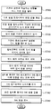
도 3은 본 발명의 다른 실시예에 따른 기판의 결함 검출 장치를 나타낸 블럭도이다.
도 4는 도 3의 장치를 이용해서 기판의 결함을 검출하는 방법을 순차적으로 나타낸 흐름도이다.
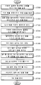
도 5는 본 발명의 또 다른 실시예에 따른 기판의 결함 검출 장치를 나타낸 블럭도이다.
도 6은 도 5의 장치를 이용해서 기판의 결함을 검출하는 방법을 순차적으로 나타낸 흐름도이다.
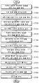
도 7은 본 발명의 또 다른 실시예에 따른 기판의 결함 검출 장치를 나타낸 블럭도이다.
도 8은 본 발명의 또 다른 실시예에 따른 기판의 결함 검출 장치를 나타낸 블럭도이다.
도 9는 도 8의 장치를 이용해서 기판의 결함을 검출하는 방법을 순차적으로 나타낸 흐름도이다.
도 10은 본 발명의 또 다른 실시예에 따른 기판의 결함 검출 장치를 나타낸 블럭도이다.
도 11은 도 10의 장치를 이용해서 기판의 결함을 검출하는 방법을 순차적으로 나타낸 흐름도이다.
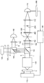
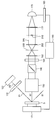
I ; 입사 빔 R ; 반사 빔
110 ; 스테이지 120 ; 광원
130 ; 편광기 140 ; 필터
150 ; 대물 렌즈 160 ; 이미지 센서
170 ; 검출부 180 ; 분석부
185 ; 증폭부 190 ; 분석기
200 ; 공간 필터 210 ; 차단판
Claims (20)
- 기판의 표면으로 입사 빔을 조사하고 그리고
상기 입사 빔에 의해서 상기 기판의 표면으로부터 발생된 반사 빔 중에서 상기 기판의 표면에 위치한 결함에 기인한 제 2 고조파수(Second Harmonic Generation : SHG) 빔을 검출하는 것을 포함하는 기판의 결함 검출 방법. - 제 1 항에 있어서, 상기 기판의 표면과 평행한 방향을 따라 기초 빔을 발생시키는 것을 더 포함하는 기판의 결함 검출 방법.
- 제 2 항에 있어서, 상기 기초 빔은 스팟(spot) 빔 또는 라인(line) 빔을 포함하는 기판의 결함 검출 방법.
- 제 2 항에 있어서, 상기 기초 빔은 하나 이상의 주파수를 갖는 기판의 결함 검출 방법.
- 제 2 항에 있어서, 상기 기초 빔을 편광시켜서 편광 빔을 형성하는 것을 더 포함하는 기판의 결함 검출 방법.
- 제 5 항에 있어서, 상기 편광 빔을 상기 기판의 표면을 향해서 반사시켜서 상기 기판의 표면으로 상기 표면과 직교하는 방향을 따라 입사되는 상기 입사 빔을 형성하는 것을 더 포함하는 기판의 결함 검출 방법.
- 제 1 항에 있어서, 상기 SHG 빔을 검출하는 것은 상기 반사 빔 중에서 상기 SHG 빔의 주파수 대역을 벗어난 주파수 대역에 속하는 반사 빔을 제거하는 것을 포함하는 기판의 결함 검출 방법.
- 제 1 항에 있어서, 상기 SHG 빔을 검출하는 것은 상기 반사 빔 중에서 상기 SHG 빔의 방향과 다른 방향을 갖는 반사 빔을 제거하는 것을 포함하는 기판의 결함 검출 방법.
- 제 1 항에 있어서, 상기 SHG 빔을 검출하는 것은 상기 SHG 빔으로부터 노이즈를 제거하는 것을 포함하는 기판의 결함 검출 방법.
- 제 1 항에 있어서, 상기 SHG 빔을 검출하는 것은 상기 반사 빔 중에서 상기 기판의 표면에 기인한 반사 빔의 진행을 차단하는 것을 포함하는 기판의 결함 검출 방법.
- 제 1 항에 있어서, 상기 반사 빔을 이용해서 상기 입사 빔을 상기 기판의 표면에 대해서 포커싱하는 것을 더 포함하는 기판의 결함 검출 방법.
- 제 1 항에 있어서, 상기 SHG 빔을 분석하여, 상기 결함의 위치, 크기 및 물성에 대한 정보를 획득하는 것을 더 포함하는 기판의 결함 검출 방법.
- 기판의 표면으로 입사되는 입사 빔을 발생시키는 광원
상기 입사 빔에 의해서 상기 기판의 표면으로부터 발생된 반사 빔 중에서 상기 기판의 표면에 위치한 결함에 기인한 제 2 고조파수(Second Harmonic Generation : SHG) 빔을 통과시키는 필터 및
상기 필터를 통과한 상기 SHG 빔을 검출하는 검출부를 포함하는 기판의 결함 검출 장치. - 제 13 항에 있어서, 상기 광원은 상기 기판의 표면과 평행한 방향을 따라 기초 빔을 발생시키는 기판의 결함 검출 장치.
- 제 13 항에 있어서, 상기 기초 빔을 편광시켜서 편광 빔을 형성하는 편광기(polarizer)를 더 포함하는 기판의 결함 검출 장치.
- 제 13 항에 있어서, 상기 필터는 상기 편광 빔을 상기 기판의 표면을 향해서 반사시켜서 상기 기판의 표면으로 상기 표면과 직교하는 방향을 따라 입사되는 상기 입사 빔을 형성하는 다이크로익 미러(dichroic mirror)를 포함하는 기판의 결함 검출 장치.
- 제 13 항에 있어서, 상기 반사 빔 중에서 상기 SHG 빔의 방향과 다른 방향을 갖는 반사 빔을 제거하는 분석기(analyzer)를 더 포함하는 기판의 결함 검출 장치.
- 제 13 항에 있어서, 상기 SHG 빔으로부터 노이즈를 제거하는 공간 필터(spatial filter)를 더 포함하는 기판의 결함 검출 장치.
- 제 13 항에 있어서, 상기 반사 빔 중에서 상기 기판의 표면에 기인한 반사 빔의 진행을 차단하는 차단판을 더 포함하는 기판의 결함 검출 장치.
- 제 13 항에 있어서, 상기 반사 빔을 이용해서 상기 입사 빔을 상기 기판의 표면에 대해서 포커싱하는 이미지 센서를 더 포함하는 기판의 결함 검출 장치.
Priority Applications (3)
| Application Number | Priority Date | Filing Date | Title |
|---|---|---|---|
| KR1020180111663A KR102750068B1 (ko) | 2018-09-18 | 2018-09-18 | 기판의 결함 검출 방법 및 이를 수행하기 위한 장치 |
| US16/364,251 US10816480B2 (en) | 2018-09-18 | 2019-03-26 | Method of detecting a defect on a substrate, apparatus for performing the same and method of manufacturing semiconductor device using the same |
| CN201910542195.5A CN110907471B (zh) | 2018-09-18 | 2019-06-21 | 检测基板上的缺陷的方法和用于检测基板上的缺陷的设备 |
Applications Claiming Priority (1)
| Application Number | Priority Date | Filing Date | Title |
|---|---|---|---|
| KR1020180111663A KR102750068B1 (ko) | 2018-09-18 | 2018-09-18 | 기판의 결함 검출 방법 및 이를 수행하기 위한 장치 |
Publications (2)
| Publication Number | Publication Date |
|---|---|
| KR20200032801A true KR20200032801A (ko) | 2020-03-27 |
| KR102750068B1 KR102750068B1 (ko) | 2025-01-03 |
Family
ID=69772138
Family Applications (1)
| Application Number | Title | Priority Date | Filing Date |
|---|---|---|---|
| KR1020180111663A Active KR102750068B1 (ko) | 2018-09-18 | 2018-09-18 | 기판의 결함 검출 방법 및 이를 수행하기 위한 장치 |
Country Status (3)
| Country | Link |
|---|---|
| US (1) | US10816480B2 (ko) |
| KR (1) | KR102750068B1 (ko) |
| CN (1) | CN110907471B (ko) |
Cited By (2)
| Publication number | Priority date | Publication date | Assignee | Title |
|---|---|---|---|---|
| WO2022241141A1 (en) * | 2021-05-12 | 2022-11-17 | Femtometrix, Inc. | Second-harmonic generation for critical dimensional metrology |
| WO2024220375A1 (en) * | 2023-04-18 | 2024-10-24 | Kla Corporation | Methods and systems for nanoscale imaging based on second harmonic signal generation and through-focus scanning optical microscopy |
Families Citing this family (5)
| Publication number | Priority date | Publication date | Assignee | Title |
|---|---|---|---|---|
| JP7181051B2 (ja) * | 2018-10-18 | 2022-11-30 | シャープ株式会社 | 原稿搬送装置および画像形成装置 |
| CN112485272B (zh) * | 2020-12-14 | 2021-11-09 | 紫创(南京)科技有限公司 | 半导体检测装置及检测方法 |
| CN114577726B (zh) * | 2022-03-14 | 2025-09-02 | 中国科学院微电子研究所 | 二次谐波表征方法、基于其的表征光学系统及检测装置 |
| CN114823406B (zh) * | 2022-03-31 | 2023-03-24 | 上海微崇半导体设备有限公司 | 一种基于二次谐波测量半导体多层结构的方法和装置 |
| JP2024080718A (ja) | 2022-12-05 | 2024-06-17 | 三星電子株式会社 | 対象物の表面を検査する装置 |
Citations (5)
| Publication number | Priority date | Publication date | Assignee | Title |
|---|---|---|---|---|
| US5294289A (en) * | 1990-10-30 | 1994-03-15 | International Business Machines Corporation | Detection of interfaces with atomic resolution during material processing by optical second harmonic generation |
| JP2006029881A (ja) * | 2004-07-14 | 2006-02-02 | Hitachi High-Technologies Corp | パターン欠陥検査方法および装置 |
| US20150330908A1 (en) * | 2014-04-17 | 2015-11-19 | Femtometrix, Inc. | Pump and probe type second harmonic generation metrology |
| US20160240993A1 (en) * | 2013-10-25 | 2016-08-18 | Nikon Corporation | Laser device, and exposure device and inspection device provided with the laser device |
| KR20170092573A (ko) * | 2014-11-12 | 2017-08-11 | 펨토매트릭스, 인코포레이티드. | 제2고조파 발생(shg) 신호 내에서 재료 특성을 해석하는 시스템 |
Family Cites Families (9)
| Publication number | Priority date | Publication date | Assignee | Title |
|---|---|---|---|---|
| JPH07260702A (ja) | 1994-03-24 | 1995-10-13 | Nec Corp | 界面検査方法およびその装置 |
| JPH07318500A (ja) * | 1994-05-23 | 1995-12-08 | Hitachi Ltd | 物体表面近傍の検査装置 |
| US6791099B2 (en) | 2001-02-14 | 2004-09-14 | Applied Materials, Inc. | Laser scanning wafer inspection using nonlinear optical phenomena |
| JP3996774B2 (ja) | 2002-01-09 | 2007-10-24 | 株式会社日立ハイテクノロジーズ | パターン欠陥検査方法及びパターン欠陥検査装置 |
| JP2010085225A (ja) | 2008-09-30 | 2010-04-15 | Epson Toyocom Corp | 圧電振動片ウェハのエッチング欠陥検査方法、及び検査システム |
| CN102095690A (zh) * | 2010-12-20 | 2011-06-15 | 福建师范大学 | 一种偏振成像的无损探测装置 |
| CN104655592A (zh) * | 2013-11-19 | 2015-05-27 | 有研光电新材料有限责任公司 | 一种测试激光倍频晶体性质的装置和方法 |
| US9632020B2 (en) | 2014-10-22 | 2017-04-25 | The Boeing Company | Non-linear optical ellipsometry for surface monitoring and characterization |
| US10928329B2 (en) * | 2017-10-11 | 2021-02-23 | Board Of Regents, The University Of Texas System | Method and system for optically detecting and characterizing defects in semiconductors |
-
2018
- 2018-09-18 KR KR1020180111663A patent/KR102750068B1/ko active Active
-
2019
- 2019-03-26 US US16/364,251 patent/US10816480B2/en active Active
- 2019-06-21 CN CN201910542195.5A patent/CN110907471B/zh active Active
Patent Citations (5)
| Publication number | Priority date | Publication date | Assignee | Title |
|---|---|---|---|---|
| US5294289A (en) * | 1990-10-30 | 1994-03-15 | International Business Machines Corporation | Detection of interfaces with atomic resolution during material processing by optical second harmonic generation |
| JP2006029881A (ja) * | 2004-07-14 | 2006-02-02 | Hitachi High-Technologies Corp | パターン欠陥検査方法および装置 |
| US20160240993A1 (en) * | 2013-10-25 | 2016-08-18 | Nikon Corporation | Laser device, and exposure device and inspection device provided with the laser device |
| US20150330908A1 (en) * | 2014-04-17 | 2015-11-19 | Femtometrix, Inc. | Pump and probe type second harmonic generation metrology |
| KR20170092573A (ko) * | 2014-11-12 | 2017-08-11 | 펨토매트릭스, 인코포레이티드. | 제2고조파 발생(shg) 신호 내에서 재료 특성을 해석하는 시스템 |
Cited By (3)
| Publication number | Priority date | Publication date | Assignee | Title |
|---|---|---|---|---|
| WO2022241141A1 (en) * | 2021-05-12 | 2022-11-17 | Femtometrix, Inc. | Second-harmonic generation for critical dimensional metrology |
| US12553708B2 (en) | 2021-05-12 | 2026-02-17 | Femtometrix, Inc. | Second-harmonic generation for critical dimensional metrology |
| WO2024220375A1 (en) * | 2023-04-18 | 2024-10-24 | Kla Corporation | Methods and systems for nanoscale imaging based on second harmonic signal generation and through-focus scanning optical microscopy |
Also Published As
| Publication number | Publication date |
|---|---|
| CN110907471A (zh) | 2020-03-24 |
| US20200088649A1 (en) | 2020-03-19 |
| CN110907471B (zh) | 2024-10-29 |
| KR102750068B1 (ko) | 2025-01-03 |
| US10816480B2 (en) | 2020-10-27 |
Similar Documents
| Publication | Publication Date | Title |
|---|---|---|
| KR102750068B1 (ko) | 기판의 결함 검출 방법 및 이를 수행하기 위한 장치 | |
| US9970883B2 (en) | Multi-spot scanning collection optics | |
| JP5268061B2 (ja) | 基板検査装置 | |
| JP3978528B2 (ja) | パターン欠陥検査装置及びレーザ顕微鏡 | |
| CN103674926A (zh) | 光学装置 | |
| JP2012026733A (ja) | 光学式欠陥検出装置及び方法並びにこれを備えた欠陥観察装置 | |
| US9976903B2 (en) | Spectrometer and method of spectroscopy | |
| CN108732155B (zh) | 拉曼探头 | |
| CN106233125A (zh) | 共聚焦线检验光学系统 | |
| WO2024220375A1 (en) | Methods and systems for nanoscale imaging based on second harmonic signal generation and through-focus scanning optical microscopy | |
| JP3282790B2 (ja) | 位相シフトマスクの欠陥検査装置 | |
| CN115668289A (zh) | 通过组合来自多个收集通道的信息的设计与晶片图像相关性 | |
| JP2016015371A (ja) | 厚さ測定装置、厚さ測定方法及び露光装置 | |
| JP4890039B2 (ja) | 共焦点型撮像装置 | |
| TW202138750A (zh) | 光學臨界尺寸與光反射組合裝置、系統及方法 | |
| KR20210156209A (ko) | 레이저 가공 장치의 검사 방법 | |
| JP2026500590A (ja) | 二次高調波生成を用いる界面依拠欠陥検査 | |
| JP2015224912A (ja) | 欠陥測定装置及び欠陥測定方法 | |
| JP4961615B2 (ja) | フォトマスクの検査方法及び装置 | |
| JP2018054353A (ja) | 近接場顕微鏡 | |
| US20240219314A1 (en) | Optical measurement apparatus, optical measurement method using the same, and method for manufacturing semiconductor device using the same | |
| US12204081B1 (en) | Dark-field confocal microscopy measurement apparatus and method based on time-varying fractional-order vortex demodulation | |
| TWI853252B (zh) | 彩色光學檢測裝置及包括其的系統 | |
| JP2020188142A (ja) | 結晶欠陥検出装置及び結晶欠陥検出方法 | |
| TW202544441A (zh) | 基於時間解析非聲學信號的計量 |
Legal Events
| Date | Code | Title | Description |
|---|---|---|---|
| PA0109 | Patent application |
St.27 status event code: A-0-1-A10-A12-nap-PA0109 |
|
| P11-X000 | Amendment of application requested |
St.27 status event code: A-2-2-P10-P11-nap-X000 |
|
| P13-X000 | Application amended |
St.27 status event code: A-2-2-P10-P13-nap-X000 |
|
| R15-X000 | Change to inventor requested |
St.27 status event code: A-3-3-R10-R15-oth-X000 |
|
| R16-X000 | Change to inventor recorded |
St.27 status event code: A-3-3-R10-R16-oth-X000 |
|
| PG1501 | Laying open of application |
St.27 status event code: A-1-1-Q10-Q12-nap-PG1501 |
|
| A201 | Request for examination | ||
| PA0201 | Request for examination |
St.27 status event code: A-1-2-D10-D11-exm-PA0201 |
|
| D13-X000 | Search requested |
St.27 status event code: A-1-2-D10-D13-srh-X000 |
|
| D14-X000 | Search report completed |
St.27 status event code: A-1-2-D10-D14-srh-X000 |
|
| E902 | Notification of reason for refusal | ||
| PE0902 | Notice of grounds for rejection |
St.27 status event code: A-1-2-D10-D21-exm-PE0902 |
|
| E13-X000 | Pre-grant limitation requested |
St.27 status event code: A-2-3-E10-E13-lim-X000 |
|
| P11-X000 | Amendment of application requested |
St.27 status event code: A-2-2-P10-P11-nap-X000 |
|
| P13-X000 | Application amended |
St.27 status event code: A-2-2-P10-P13-nap-X000 |
|
| PE0601 | Decision on rejection of patent |
St.27 status event code: N-2-6-B10-B15-exm-PE0601 |
|
| E13-X000 | Pre-grant limitation requested |
St.27 status event code: A-2-3-E10-E13-lim-X000 |
|
| P11-X000 | Amendment of application requested |
St.27 status event code: A-2-2-P10-P11-nap-X000 |
|
| P13-X000 | Application amended |
St.27 status event code: A-2-2-P10-P13-nap-X000 |
|
| PX0901 | Re-examination |
St.27 status event code: A-2-3-E10-E12-rex-PX0901 |
|
| PX0701 | Decision of registration after re-examination |
St.27 status event code: A-3-4-F10-F13-rex-PX0701 |
|
| X701 | Decision to grant (after re-examination) | ||
| GRNT | Written decision to grant | ||
| PR0701 | Registration of establishment |
St.27 status event code: A-2-4-F10-F11-exm-PR0701 |
|
| PR1002 | Payment of registration fee |
St.27 status event code: A-2-2-U10-U11-oth-PR1002 Fee payment year number: 1 |
|
| PG1601 | Publication of registration |
St.27 status event code: A-4-4-Q10-Q13-nap-PG1601 |
|
| P22-X000 | Classification modified |
St.27 status event code: A-4-4-P10-P22-nap-X000 |