KR20200032809A - Display device and manufacturing method of same - Google Patents
Display device and manufacturing method of same Download PDFInfo
- Publication number
- KR20200032809A KR20200032809A KR1020180111827A KR20180111827A KR20200032809A KR 20200032809 A KR20200032809 A KR 20200032809A KR 1020180111827 A KR1020180111827 A KR 1020180111827A KR 20180111827 A KR20180111827 A KR 20180111827A KR 20200032809 A KR20200032809 A KR 20200032809A
- Authority
- KR
- South Korea
- Prior art keywords
- pixel electrode
- pixel
- wiring
- disposed
- light emitting
- Prior art date
- Legal status (The legal status is an assumption and is not a legal conclusion. Google has not performed a legal analysis and makes no representation as to the accuracy of the status listed.)
- Granted
Links
Images









Classifications
-
- H—ELECTRICITY
- H10—SEMICONDUCTOR DEVICES; ELECTRIC SOLID-STATE DEVICES NOT OTHERWISE PROVIDED FOR
- H10H—INORGANIC LIGHT-EMITTING SEMICONDUCTOR DEVICES HAVING POTENTIAL BARRIERS
- H10H29/00—Integrated devices, or assemblies of multiple devices, comprising at least one light-emitting semiconductor element covered by group H10H20/00
- H10H29/01—Manufacture or treatment
- H10H29/03—Manufacture or treatment using mass transfer of LEDs, e.g. by using liquid suspensions
-
- H—ELECTRICITY
- H10—SEMICONDUCTOR DEVICES; ELECTRIC SOLID-STATE DEVICES NOT OTHERWISE PROVIDED FOR
- H10H—INORGANIC LIGHT-EMITTING SEMICONDUCTOR DEVICES HAVING POTENTIAL BARRIERS
- H10H29/00—Integrated devices, or assemblies of multiple devices, comprising at least one light-emitting semiconductor element covered by group H10H20/00
- H10H29/10—Integrated devices comprising at least one light-emitting semiconductor component covered by group H10H20/00
- H10H29/14—Integrated devices comprising at least one light-emitting semiconductor component covered by group H10H20/00 comprising multiple light-emitting semiconductor components
- H10H29/142—Two-dimensional arrangements, e.g. asymmetric LED layout
-
- G—PHYSICS
- G09—EDUCATION; CRYPTOGRAPHY; DISPLAY; ADVERTISING; SEALS
- G09G—ARRANGEMENTS OR CIRCUITS FOR CONTROL OF INDICATING DEVICES USING STATIC MEANS TO PRESENT VARIABLE INFORMATION
- G09G3/00—Control arrangements or circuits, of interest only in connection with visual indicators other than cathode-ray tubes
- G09G3/20—Control arrangements or circuits, of interest only in connection with visual indicators other than cathode-ray tubes for presentation of an assembly of a number of characters, e.g. a page, by composing the assembly by combination of individual elements arranged in a matrix no fixed position being assigned to or needed to be assigned to the individual characters or partial characters
- G09G3/22—Control arrangements or circuits, of interest only in connection with visual indicators other than cathode-ray tubes for presentation of an assembly of a number of characters, e.g. a page, by composing the assembly by combination of individual elements arranged in a matrix no fixed position being assigned to or needed to be assigned to the individual characters or partial characters using controlled light sources
- G09G3/30—Control arrangements or circuits, of interest only in connection with visual indicators other than cathode-ray tubes for presentation of an assembly of a number of characters, e.g. a page, by composing the assembly by combination of individual elements arranged in a matrix no fixed position being assigned to or needed to be assigned to the individual characters or partial characters using controlled light sources using electroluminescent panels
- G09G3/32—Control arrangements or circuits, of interest only in connection with visual indicators other than cathode-ray tubes for presentation of an assembly of a number of characters, e.g. a page, by composing the assembly by combination of individual elements arranged in a matrix no fixed position being assigned to or needed to be assigned to the individual characters or partial characters using controlled light sources using electroluminescent panels semiconductive, e.g. using light-emitting diodes [LED]
-
- H01L27/1214—
-
- H01L27/156—
-
- H01L33/005—
-
- H01L33/36—
-
- H01L33/62—
-
- H—ELECTRICITY
- H10—SEMICONDUCTOR DEVICES; ELECTRIC SOLID-STATE DEVICES NOT OTHERWISE PROVIDED FOR
- H10D—INORGANIC ELECTRIC SEMICONDUCTOR DEVICES
- H10D86/00—Integrated devices formed in or on insulating or conducting substrates, e.g. formed in silicon-on-insulator [SOI] substrates or on stainless steel or glass substrates
- H10D86/01—Manufacture or treatment
- H10D86/021—Manufacture or treatment of multiple TFTs
-
- H—ELECTRICITY
- H10—SEMICONDUCTOR DEVICES; ELECTRIC SOLID-STATE DEVICES NOT OTHERWISE PROVIDED FOR
- H10D—INORGANIC ELECTRIC SEMICONDUCTOR DEVICES
- H10D86/00—Integrated devices formed in or on insulating or conducting substrates, e.g. formed in silicon-on-insulator [SOI] substrates or on stainless steel or glass substrates
- H10D86/40—Integrated devices formed in or on insulating or conducting substrates, e.g. formed in silicon-on-insulator [SOI] substrates or on stainless steel or glass substrates characterised by multiple TFTs
- H10D86/441—Interconnections, e.g. scanning lines
-
- H—ELECTRICITY
- H10—SEMICONDUCTOR DEVICES; ELECTRIC SOLID-STATE DEVICES NOT OTHERWISE PROVIDED FOR
- H10H—INORGANIC LIGHT-EMITTING SEMICONDUCTOR DEVICES HAVING POTENTIAL BARRIERS
- H10H20/00—Individual inorganic light-emitting semiconductor devices having potential barriers, e.g. light-emitting diodes [LED]
- H10H20/01—Manufacture or treatment
-
- H—ELECTRICITY
- H10—SEMICONDUCTOR DEVICES; ELECTRIC SOLID-STATE DEVICES NOT OTHERWISE PROVIDED FOR
- H10H—INORGANIC LIGHT-EMITTING SEMICONDUCTOR DEVICES HAVING POTENTIAL BARRIERS
- H10H20/00—Individual inorganic light-emitting semiconductor devices having potential barriers, e.g. light-emitting diodes [LED]
- H10H20/80—Constructional details
- H10H20/85—Packages
- H10H20/857—Interconnections, e.g. lead-frames, bond wires or solder balls
-
- H—ELECTRICITY
- H10—SEMICONDUCTOR DEVICES; ELECTRIC SOLID-STATE DEVICES NOT OTHERWISE PROVIDED FOR
- H10H—INORGANIC LIGHT-EMITTING SEMICONDUCTOR DEVICES HAVING POTENTIAL BARRIERS
- H10H29/00—Integrated devices, or assemblies of multiple devices, comprising at least one light-emitting semiconductor element covered by group H10H20/00
- H10H29/30—Active-matrix LED displays
- H10H29/39—Connection of the pixel electrodes to the driving transistors
-
- H—ELECTRICITY
- H10—SEMICONDUCTOR DEVICES; ELECTRIC SOLID-STATE DEVICES NOT OTHERWISE PROVIDED FOR
- H10W—GENERIC PACKAGES, INTERCONNECTIONS, CONNECTORS OR OTHER CONSTRUCTIONAL DETAILS OF DEVICES COVERED BY CLASS H10
- H10W90/00—Package configurations
-
- G—PHYSICS
- G09—EDUCATION; CRYPTOGRAPHY; DISPLAY; ADVERTISING; SEALS
- G09G—ARRANGEMENTS OR CIRCUITS FOR CONTROL OF INDICATING DEVICES USING STATIC MEANS TO PRESENT VARIABLE INFORMATION
- G09G2300/00—Aspects of the constitution of display devices
- G09G2300/04—Structural and physical details of display devices
- G09G2300/0404—Matrix technologies
- G09G2300/0413—Details of dummy pixels or dummy lines in flat panels
-
- G—PHYSICS
- G09—EDUCATION; CRYPTOGRAPHY; DISPLAY; ADVERTISING; SEALS
- G09G—ARRANGEMENTS OR CIRCUITS FOR CONTROL OF INDICATING DEVICES USING STATIC MEANS TO PRESENT VARIABLE INFORMATION
- G09G2310/00—Command of the display device
- G09G2310/02—Addressing, scanning or driving the display screen or processing steps related thereto
- G09G2310/0264—Details of driving circuits
- G09G2310/0267—Details of drivers for scan electrodes, other than drivers for liquid crystal, plasma or OLED displays
-
- G—PHYSICS
- G09—EDUCATION; CRYPTOGRAPHY; DISPLAY; ADVERTISING; SEALS
- G09G—ARRANGEMENTS OR CIRCUITS FOR CONTROL OF INDICATING DEVICES USING STATIC MEANS TO PRESENT VARIABLE INFORMATION
- G09G2330/00—Aspects of power supply; Aspects of display protection and defect management
- G09G2330/02—Details of power systems and of start or stop of display operation
- G09G2330/028—Generation of voltages supplied to electrode drivers in a matrix display other than LCD
-
- H—ELECTRICITY
- H10—SEMICONDUCTOR DEVICES; ELECTRIC SOLID-STATE DEVICES NOT OTHERWISE PROVIDED FOR
- H10D—INORGANIC ELECTRIC SEMICONDUCTOR DEVICES
- H10D86/00—Integrated devices formed in or on insulating or conducting substrates, e.g. formed in silicon-on-insulator [SOI] substrates or on stainless steel or glass substrates
- H10D86/40—Integrated devices formed in or on insulating or conducting substrates, e.g. formed in silicon-on-insulator [SOI] substrates or on stainless steel or glass substrates characterised by multiple TFTs
- H10D86/451—Integrated devices formed in or on insulating or conducting substrates, e.g. formed in silicon-on-insulator [SOI] substrates or on stainless steel or glass substrates characterised by multiple TFTs characterised by the compositions or shapes of the interlayer dielectrics
-
- H—ELECTRICITY
- H10—SEMICONDUCTOR DEVICES; ELECTRIC SOLID-STATE DEVICES NOT OTHERWISE PROVIDED FOR
- H10D—INORGANIC ELECTRIC SEMICONDUCTOR DEVICES
- H10D86/00—Integrated devices formed in or on insulating or conducting substrates, e.g. formed in silicon-on-insulator [SOI] substrates or on stainless steel or glass substrates
- H10D86/40—Integrated devices formed in or on insulating or conducting substrates, e.g. formed in silicon-on-insulator [SOI] substrates or on stainless steel or glass substrates characterised by multiple TFTs
- H10D86/60—Integrated devices formed in or on insulating or conducting substrates, e.g. formed in silicon-on-insulator [SOI] substrates or on stainless steel or glass substrates characterised by multiple TFTs wherein the TFTs are in active matrices
-
- H—ELECTRICITY
- H10—SEMICONDUCTOR DEVICES; ELECTRIC SOLID-STATE DEVICES NOT OTHERWISE PROVIDED FOR
- H10H—INORGANIC LIGHT-EMITTING SEMICONDUCTOR DEVICES HAVING POTENTIAL BARRIERS
- H10H20/00—Individual inorganic light-emitting semiconductor devices having potential barriers, e.g. light-emitting diodes [LED]
- H10H20/01—Manufacture or treatment
- H10H20/036—Manufacture or treatment of packages
- H10H20/0364—Manufacture or treatment of packages of interconnections
-
- H—ELECTRICITY
- H10—SEMICONDUCTOR DEVICES; ELECTRIC SOLID-STATE DEVICES NOT OTHERWISE PROVIDED FOR
- H10H—INORGANIC LIGHT-EMITTING SEMICONDUCTOR DEVICES HAVING POTENTIAL BARRIERS
- H10H29/00—Integrated devices, or assemblies of multiple devices, comprising at least one light-emitting semiconductor element covered by group H10H20/00
- H10H29/01—Manufacture or treatment
- H10H29/032—Manufacture or treatment of electrodes
-
- H—ELECTRICITY
- H10—SEMICONDUCTOR DEVICES; ELECTRIC SOLID-STATE DEVICES NOT OTHERWISE PROVIDED FOR
- H10H—INORGANIC LIGHT-EMITTING SEMICONDUCTOR DEVICES HAVING POTENTIAL BARRIERS
- H10H29/00—Integrated devices, or assemblies of multiple devices, comprising at least one light-emitting semiconductor element covered by group H10H20/00
- H10H29/30—Active-matrix LED displays
- H10H29/41—Insulating layers formed between the driving transistors and the LEDs
-
- H—ELECTRICITY
- H10—SEMICONDUCTOR DEVICES; ELECTRIC SOLID-STATE DEVICES NOT OTHERWISE PROVIDED FOR
- H10H—INORGANIC LIGHT-EMITTING SEMICONDUCTOR DEVICES HAVING POTENTIAL BARRIERS
- H10H29/00—Integrated devices, or assemblies of multiple devices, comprising at least one light-emitting semiconductor element covered by group H10H20/00
- H10H29/30—Active-matrix LED displays
- H10H29/49—Interconnections, e.g. wiring lines or terminals
Landscapes
- Engineering & Computer Science (AREA)
- Physics & Mathematics (AREA)
- Computer Hardware Design (AREA)
- General Physics & Mathematics (AREA)
- Theoretical Computer Science (AREA)
- Devices For Indicating Variable Information By Combining Individual Elements (AREA)
- Electroluminescent Light Sources (AREA)
- Manufacturing & Machinery (AREA)
Abstract
표시 장치의 제조 방법은, 복수의 화소 영역들을 포함하는 표시 영역과, 표시 영역의 외곽에 배치되는 비표시 영역을 포함하는 기판을 준비한다. 화소 영역들 각각에 제1 스위칭 소자를 형성하고, 비표시 영역에 배치되되 제1 스위칭 소자와 전기적으로 연결되는 기준 전압 배선을 포함하는 회로소자층을 형성한다. 회소소자층 상의 화소 영역들 각각에 배치되고 제1 스위칭 소자를 통해 기준 전압 배선에 전기적으로 연결되는 제1 화소 전극, 및 제1 화소 전극에 대향하는 제2 화소 전극을 포함하는 화소 전극들을 형성한다. 제1 화소 전극 및 제2 화소 전극 사이에 복수의 발광 소자들을 배치한다. 기준 전압 배선에 제1 전원전압을 인가하고 제2 화소 전극에 제2 전원전압을 인가하여 발광 소자들을 정렬한다.In a manufacturing method of a display device, a display area including a plurality of pixel areas and a substrate including a non-display area disposed outside the display area are prepared. A first switching element is formed in each of the pixel areas, and a circuit element layer is disposed in the non-display area and includes a reference voltage wiring electrically connected to the first switching element. Pixel electrodes including first pixel electrodes disposed in each of the pixel regions on the element layer and electrically connected to the reference voltage wiring through the first switching element and second pixel electrodes facing the first pixel electrode are formed. . A plurality of light emitting elements are disposed between the first pixel electrode and the second pixel electrode. The first power voltage is applied to the reference voltage wiring and the second power voltage is applied to the second pixel electrode to align the light emitting elements.
Description
본 발명은 발광 다이오드를 포함하는 표시 장치 및 이의 제조 방법에 관한 것이다.The present invention relates to a display device including a light emitting diode and a method for manufacturing the same.
표시 장치는 발광 다이오드(Light Emitting Diode)와 같은 발광 소자를 화소의 광원으로 이용하여 고화질의 영상을 표시한다. 발광 다이오드는 열악한 환경 조건에서도 비교적 양호한 내구성을 나타내며, 수명 및 휘도 측면에서도 우수한 성능을 나타낸다.The display device displays a high-quality image by using a light emitting element such as a light emitting diode as a light source of pixels. The light emitting diode exhibits relatively good durability even in harsh environmental conditions, and exhibits excellent performance in terms of life and luminance.
최근, 신뢰성이 높은 무기 결정 구조의 재료를 이용하여 초소형의 발광 다이오드를 제조하고, 이를 표시 패널에 배치하여 차세대 화소 광원으로 이용하기 위한 연구가 진행되고 있다. 이러한 연구의 일환으로서, 마이크로 스케일 또는 나노 스케일 정도로 작은 초소형의 발광 다이오드를 제조하고, 이를 각 화소의 광원으로 이용하는 발광 표시 장치에 대한 개발이 진행되고 있다.In recent years, research has been conducted to manufacture ultra-small light-emitting diodes using a highly reliable inorganic crystal structure material, and to arrange them on a display panel for use as a next-generation pixel light source. As part of such research, development of light-emitting display devices that manufacture micro light-emitting diodes as small as micro-scale or nano-scale and use them as a light source for each pixel is underway.
본 발명이 해결하고자 하는 과제는, 발광 소자들을 용이하게 정렬하고 제조 효율을 높일 수 있는 표시 장치 및 그의 제조 방법을 제공하는 것이다.The problem to be solved by the present invention is to provide a display device and a method for manufacturing the same, which can easily align light emitting elements and increase manufacturing efficiency.
본 발명의 과제들은 이상에서 언급한 기술적 과제로 제한되지 않으며, 언급되지 않은 또 다른 기술적 과제들은 아래의 기재로부터 당업자에게 명확하게 이해될 수 있을 것이다.The problems of the present invention are not limited to the technical problems mentioned above, and other technical problems that are not mentioned will be clearly understood by those skilled in the art from the following description.
상기 과제를 해결하기 위한 본 발명의 일 실시예에 따른 표시 장치의 제조 방법은, 복수의 화소 영역들을 포함하는 표시 영역과, 상기 표시 영역의 외곽에 배치되는 비표시 영역을 포함하는 기판을 준비하는 단계; 상기 화소 영역들 각각에 제1 스위칭 소자를 형성하고, 상기 비표시 영역에 배치되되 상기 제1 스위칭 소자와 전기적으로 연결되는 기준 전압 배선을 포함하는 회로소자층을 형성하는 단계; 상기 회소소자층 상의 화소 영역들 각각에 배치되고 상기 제1 스위칭 소자를 통해 상기 기준 전압 배선에 전기적으로 연결되는 제1 화소 전극, 및 상기 제1 화소 전극에 대향하는 제2 화소 전극을 포함하는 화소 전극들을 형성하는 단계; 상기 제1 화소 전극 및 상기 제2 화소 전극 사이에 복수의 발광 소자들을 배치하는 단계; 및 상기 기준 전압 배선에 제1 전원전압을 인가하고 상기 제2 화소 전극에 제2 전원전압을 인가하여 상기 발광 소자들을 정렬하는 단계를 포함한다.A method of manufacturing a display device according to an exemplary embodiment of the present invention for solving the above problems is to prepare a substrate including a display area including a plurality of pixel areas and a non-display area disposed outside the display area. step; Forming a first switching element in each of the pixel areas, and forming a circuit element layer disposed in the non-display area and including a reference voltage wiring electrically connected to the first switching element; A pixel including a first pixel electrode disposed in each of the pixel areas on the element layer and electrically connected to the reference voltage line through the first switching element, and a second pixel electrode facing the first pixel electrode Forming electrodes; Arranging a plurality of light emitting elements between the first pixel electrode and the second pixel electrode; And aligning the light emitting elements by applying a first power voltage to the reference voltage wiring and applying a second power voltage to the second pixel electrode.
상기 방법은, 상기 발광 소자들 각각의 제1 단부 상에 배치되어 상기 발광 소자들 각각을 상기 제1 화소 전극과 연결하는 제1 컨택 전극들을 형성하는 단계; 및 상기 발광 소자들 각각의 제2 단부 상에 배치되어 상기 발광 소자들 각각을 상기 제2 화소 전극에 연결하는 제2 컨택 전극들을 형성하는 단계를 더 포함할 수 있다.The method includes forming first contact electrodes disposed on a first end of each of the light emitting elements to connect each of the light emitting elements to the first pixel electrode; And forming second contact electrodes disposed on the second end of each of the light emitting elements to connect each of the light emitting elements to the second pixel electrode.
상기 방법은, 상기 발광 소자들을 정렬하는 단계와 상기 제1 컨택 전극을 형성하는 단계 사이에 에칭 공정을 포함하지 않을 수 있다.The method may not include an etching process between aligning the light emitting elements and forming the first contact electrode.
상기 발광 소자들을 정렬하는 단계는, 상기 제1 스위칭 소자를 턴온시키는 제1 제어 신호를 상기 제1 스위칭 소자의 제어 전극에 인가하는 단계를 포함할 수 있다.Aligning the light emitting elements may include applying a first control signal to turn on the first switching element to the control electrode of the first switching element.
상기 회로소자층은 상기 제1 화소 전극 및 제1 전원단 사이에 연결되는 제2 스위칭 소자, 및 상기 제2 스위칭 소자의 제어 전극과 데이터 베선 사이에 연결되는 제3 스위칭 소자를 더 포함할 수 있다.The circuit element layer may further include a second switching element connected between the first pixel electrode and the first power terminal, and a third switching element connected between the control electrode and the data line of the second switching element. .
상기 발광 소자들을 정렬하는 단계는, 상기 제2 스위칭 소자 및 상기 제3 스위칭 소자를 각각 턴온시키는 단계를 더 포함하고, 상기 데이터 배선에는 상기 제2 스위칭 소자를 턴온시키는 턴온 전압이 인가되고, 상기 제1 전원단에는 제1 전원전압이 인가될 수 있다.The step of aligning the light emitting elements further includes turning on the second switching element and the third switching element, respectively, and a turn-on voltage for turning on the second switching element is applied to the data wiring. A first power voltage may be applied to one power terminal.
상기 회로소자층은, 상기 제1 화소 전극 및 상기 제2 스위칭 소자의 상기 제어 전극 사이에 연결되는 커패시터를 더 포함할 수 있다.The circuit element layer may further include a capacitor connected between the first pixel electrode and the control electrode of the second switching element.
상기 발광 소자들을 정렬하는 단계는, 상기 제3 스위칭 소자를 턴온시키는 단계를 더 포함하고, 상기 데이터 배선에 상기 제1 전원전압을 인가할 수 있다.Aligning the light emitting elements may further include turning on the third switching element, and apply the first power voltage to the data wiring.
상기 화소 전극들을 형성하는 단계는, 상기 비표시 영역에서 상기 기준 전압 배선과 연결되는 제1 배선 및 상기 제1 배선과 상기 제1 화소 전극을 연결하는 연결 전극을 형성하는 단계를 더 포함할 수 있다.The forming of the pixel electrodes may further include forming a first wiring connected to the reference voltage wiring and a connecting electrode connecting the first wiring and the first pixel electrode in the non-display area. .
상기 제1 전원전압은 상기 제1 배선을 통해 상기 기준 전압 배선에 인가될 수 있다.The first power voltage may be applied to the reference voltage wiring through the first wiring.
상기 방법은, 상기 연결 전극을 제거하여 상기 제1 배선과 상기 제1 화소 전극을 분리하는 단계를 더 포함할 수 있다.The method may further include separating the first wiring and the first pixel electrode by removing the connection electrode.
상기 회로소자층은, 상기 기판과 상기 표시소자층의 사이에 순차적으로 적층된 제1 절연층, 제2 절연층, 제3 절연층 및 제4 절연층을 더 포함할 수 있다.The circuit element layer may further include a first insulating layer, a second insulating layer, a third insulating layer, and a fourth insulating layer sequentially stacked between the substrate and the display element layer.
상기 기준 전압 배선은, 상기 제3 절연층 및 상기 제4 절연층의 사이에 배치된 제1 서브 배선; 상기 제2 절연층 및 상기 제3 절연층의 사이에 배치된 제2 서브 배선; 상기 제1 절연층 및 상기 제2 절연층의 사이에 배치된 제3 서브 배선; 및 상기 기판과 상기 제1 절연층의 사이에 배치된 제4 서브 배선; 중 적어도 하나를 포함할 수 있다.The reference voltage wiring may include: a first sub-wiring disposed between the third insulating layer and the fourth insulating layer; A second sub-wiring disposed between the second insulating layer and the third insulating layer; A third sub-wiring disposed between the first insulating layer and the second insulating layer; And a fourth sub-wiring disposed between the substrate and the first insulating layer. It may include at least one of.
상기 제1 전원 배선은 상기 회로소자층 상에 배치되고 상기 기준 전압 배선과 직접적으로 연결되는 제1 서브 전원 배선, 및 상기 제1 서브 전원 배선 상에 배치되는 제2 서브 전원 배선을 포함하고, 상기 제2 서브 전원 배선의 도전성은 상기 제1 서브 전원 배선의 도전성보다 클 수 있다.The first power wiring includes a first sub power wiring disposed on the circuit element layer and directly connected to the reference voltage wiring, and a second sub power wiring disposed on the first sub power wiring, and The conductivity of the second sub power supply wiring may be greater than that of the first sub power supply wiring.
상기 회로소자층을 형성하는 단계는, 상기 제1 스위칭 소자의 제어 전극에 연결되는 주사 신호선, 및 상기 비표시 영역에서 상기 주사 신호선과 더미 배선을 연결하는 제1 더미 스위칭 소자를 형성하는 단계를 더 포함할 수 있다.The forming of the circuit element layer may further include forming a scanning signal line connected to the control electrode of the first switching element and a first dummy switching element connecting the scanning signal line and the dummy wiring in the non-display area. It can contain.
상기 발광 소자들을 정렬하는 단계는, 상기 더미 배선에 상기 제1 스위칭 소자를 턴온시키는 턴온 전압을 인가하는 단계; 및 상기 제1 더미 스위칭 소자를 턴온시키는 단계를 포함할 수 있다.The step of aligning the light emitting elements may include applying a turn-on voltage to turn on the first switching element to the dummy wiring; And turning on the first dummy switching element.
상기 회로소자층은 상기 주사 신호선과 인접 주사 신호선을 연결하는 제2 더미 스위칭 소자를 더 포함하고, 상기 발광 소자들은 정렬하는 단계는 상기 제2 더미 스위칭 소자를 턴온시키는 단계를 더 포함할 수 있다.The circuit element layer may further include a second dummy switching element connecting the scan signal line and an adjacent scan signal line, and the aligning of the light emitting elements may further include turning on the second dummy switching element.
상기 과제를 해결하기 위한 본 발명의 다른 실시예에 따른 표시 장치는, 복수의 화소 영역들을 포함하는 표시 영역과, 상기 표시 영역의 외곽에 배치되는 비표시 영역을 포함하는 기판을 포함한다. 회로소자층은, 상기 화소 영역들 각각에 형성된 제1 스위칭 소자, 상기 비표시 영역에 배치되되 상기 제1 스위칭 소자와 전기적으로 연결되는 기준 전압 배선, 및 상기 제1 스위칭 소자의 제어 전극에 연결되는 스캔 배선을 포함한다. 표시소자층은, 상기 회소소자층 상의 화소 영역들 각각에 배치되고 상기 제1 스위칭 소자를 통해 상기 기준 전압 배선에 전기적으로 연결되는 제1 화소 전극, 및 상기 제1 화소 전극에 대향하는 배치된 제2 화소 전극, 및 상기 제1 화소 전극 및 상기 제2 화소 전극 사이에 배치된 복수의 발광 소자들을 포함한다. 상기 회로소자층은 상기 비표시 영역에 형성된 더미 배선, 상기 더미 배선과 상기 스캔 배선 사이에 연결되는 제1 더미 스위칭 소자를 더 포함한다.A display device according to another exemplary embodiment of the present invention for solving the above problems includes a display area including a plurality of pixel areas and a substrate including a non-display area disposed outside the display area. The circuit element layer may include a first switching element formed in each of the pixel areas, a reference voltage wiring disposed in the non-display area, and electrically connected to the first switching element, and connected to a control electrode of the first switching element. Includes scan wiring. The display element layer includes a first pixel electrode disposed in each of the pixel regions on the element layer and electrically connected to the reference voltage line through the first switching element, and a first pixel electrode facing the first pixel electrode. It includes a two pixel electrode and a plurality of light emitting elements disposed between the first pixel electrode and the second pixel electrode. The circuit element layer further includes a dummy wiring formed in the non-display area, and a first dummy switching element connected between the dummy wiring and the scan wiring.
상기 회로소자층은 상기 주사 신호선과 인접 주사 신호선을 연결하는 제2 더미 스위칭 소자를 더 포함할 수 있다.The circuit element layer may further include a second dummy switching element connecting the scan signal line and an adjacent scan signal line.
상기 과제를 해결하기 위한 본 발명의 또 다른 실시예에 따른 표시 장치는, 복수의 화소 영역들을 포함하는 표시 영역과, 상기 표시 영역의 외곽에 배치되는 비표시 영역을 포함하는 기판을 포함한다. 회로소자층은, 상기 화소 영역들 각각에 배치되는 회로 소자, 및 상기 비표시 영역에 배치되되 상기 회로 소자와 전기적으로 연결되는 기준 전압 배선을 포함한다. 표시소자층은, 상기 회로소자층 상의 화소 영역들 각각에 배치되는 제1 화소 전극, 상기 제1 화소 전극에 대향하여 배치되는 제2 화소 전극, 및 상기 제1 화소 전극 및 상기 제2 화소 전극 사이에 배치되는 복수의 발광 소자들을 포함한다. 상기 제2 화소 전극은 상기 제1 화소 전극을 에워싼다.A display device according to another exemplary embodiment of the present invention for solving the above problems includes a display area including a plurality of pixel areas, and a substrate including a non-display area disposed outside the display area. The circuit element layer includes a circuit element disposed in each of the pixel regions, and a reference voltage wiring disposed in the non-display region and electrically connected to the circuit element. The display element layer may include a first pixel electrode disposed in each of the pixel regions on the circuit element layer, a second pixel electrode disposed opposite the first pixel electrode, and between the first pixel electrode and the second pixel electrode. It includes a plurality of light emitting elements disposed in. The second pixel electrode surrounds the first pixel electrode.
기타 실시예의 구체적인 사항들은 상세한 설명 및 도면들에 포함되어 있다.Specific details of other embodiments are included in the detailed description and drawings.
본 발명의 실시예들에 의하면 표시 장치는, 화소 전극과 연결되는 기준 전압 배선을 통해 정렬 전압을 인가함으로써, 별도의 정렬 배선의 형성 공정이 배제되고, 표시 장치의 제조 효율이 향상될 수 있다.According to embodiments of the present invention, by applying the alignment voltage through the reference voltage wiring connected to the pixel electrode, a process of forming a separate alignment wiring is excluded, and manufacturing efficiency of the display device can be improved.
본 발명의 실시예들에 따른 효과는 이상에서 예시된 내용에 의해 제한되지 않으며, 더욱 다양한 효과들이 본 명세서 내에 포함되어 있다.The effects according to the embodiments of the present invention are not limited by the contents exemplified above, and more various effects are included in the present specification.
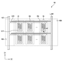
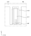
도 1은 일 실시예에 따른 표시 장치를 개략적으로 나타내는 평면도이다.
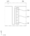
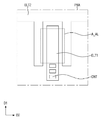
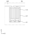
도 2 및 도 3은 본 발명의 일 실시예에 따른 표시 장치의 평면도들이다.
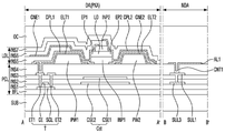
도 4는 도 3의 A-A'선 및 B-B'선을 따라 자른 표시 장치의 일 예를 나타내는 단면도이다.
도 5 내지 도 9는 도 3의 A-A'선 및 B-B'선을 따라 자른 표시 장치의 다양한 예들을 나타내는 단면도들이다.
도 10은 도 1의 표시 장치에 포함된 발광 소자의 일 예를 나타내는 사시도이다.
도 11은 도 1의 표시 장치의 일 예를 나타내는 회로도이다.
도 12는 도 11의 표시 장치에 포함된 화소의 일 예를 나타내는 회로도이다.
도 13은 도 11의 표시 장치에 포함된 데이터 구동부의 일 예를 나타내는 도면이다.
도 14은 도 12의 화소에 인가되는 신호들의 일 예를 나타내는 파형도이다.
도 15는 도 14의 표시 장치에 포함된 화소 영역에 배치되는 화소의 일 예를 나타내는 회로도이다.
도 16 및 도 17은 도 14의 표시 장치에 포함된 화소의 다른 예를 나타내는 회로도들이다.
도 18는 도 17의 화소에서 측정된 신호의 일 예를 나타내는 파형도이다.
도 19 및 도 20는 도 1의 표시 장치의 다른 일 예를 나타내는 회로도들이다.
도 21은 도 19의 표시 장치에 포함된 화소의 일 예를 나타내는 회로도이다.
도 22는 도 19의 표시 장치에 포함된 스캔 구동부의 일 예를 나타내는 회로도이다.
도 23은 도 19의 표시 장치의 다른 일 예를 나타내는 회로도이다.
도 24 내지 도 26은 도 2의 표시 장치의 다른 일 예를 나타내는 평면도들이다.
도 27 내지 도 34는 도 1의 표시 장치에 포함된 화소의 다양한 실시예를 나타내는 도면들이다.
도 35는 본 발명의 실시예들에 따른 표시 장치의 제조 방법을 나타내는 순서도이다.1 is a plan view schematically illustrating a display device according to an exemplary embodiment.
2 and 3 are plan views of a display device according to an exemplary embodiment.
4 is a cross-sectional view illustrating an example of a display device cut along the line A-A 'and B-B' of FIG. 3.
5 to 9 are cross-sectional views illustrating various examples of a display device cut along the line A-A 'and B-B' of FIG. 3.
10 is a perspective view illustrating an example of a light emitting device included in the display device of FIG. 1.
11 is a circuit diagram illustrating an example of the display device of FIG. 1.
12 is a circuit diagram illustrating an example of a pixel included in the display device of FIG. 11.
13 is a diagram illustrating an example of a data driver included in the display device of FIG. 11.
14 is a waveform diagram illustrating an example of signals applied to the pixel of FIG. 12.
15 is a circuit diagram illustrating an example of pixels arranged in a pixel area included in the display device of FIG. 14.
16 and 17 are circuit diagrams illustrating other examples of pixels included in the display device of FIG. 14.
18 is a waveform diagram illustrating an example of a signal measured in the pixel of FIG. 17.
19 and 20 are circuit diagrams illustrating another example of the display device of FIG. 1.
21 is a circuit diagram illustrating an example of a pixel included in the display device of FIG. 19.
22 is a circuit diagram illustrating an example of a scan driver included in the display device of FIG. 19.
23 is a circuit diagram illustrating another example of the display device of FIG. 19.
24 to 26 are plan views illustrating another example of the display device of FIG. 2.
27 to 34 are diagrams illustrating various embodiments of pixels included in the display device of FIG. 1.
35 is a flowchart illustrating a method of manufacturing a display device according to some example embodiments of the present invention.
본 발명의 이점 및 특징, 그리고 그것들을 달성하는 방법은 첨부되는 도면과 함께 상세하게 후술되어 있는 실시예들을 참조하면 명확해질 것이다. 그러나 본 발명은 이하에서 개시되는 실시예들에 한정되는 것이 아니라 서로 다른 다양한 형태로 구현될 것이며, 단지 본 실시예들은 본 발명의 개시가 완전하도록 하며, 본 발명이 속하는 기술분야에서 통상의 지식을 가진 자에게 발명의 범주를 완전하게 알려주기 위해 제공되는 것이며, 본 발명은 청구항의 범주에 의해 정의될 뿐이다. Advantages and features of the present invention, and methods for achieving them will be clarified with reference to embodiments described below in detail together with the accompanying drawings. However, the present invention is not limited to the embodiments disclosed below, but will be implemented in various different forms, and only the present embodiments allow the disclosure of the present invention to be complete, and the ordinary knowledge in the technical field to which the present invention pertains. It is provided to fully inform the holder of the scope of the invention, and the invention is only defined by the scope of the claims.
소자(elements) 또는 층이 다른 소자 또는 층의 "위(on)"로 지칭되는 것은 다른 소자 바로 위에 또는 중간에 다른 층 또는 다른 소자를 개재한 경우를 모두 포함한다. 명세서 전체에 걸쳐 동일 참조 부호는 동일 구성 요소를 지칭한다.An element or layer being referred to as the "on" of another element or layer includes all cases in which another layer or other element is interposed immediately above or in between. The same reference numerals refer to the same components throughout the specification.
비록 제1, 제2 등이 다양한 구성요소들을 서술하기 위해서 사용되나, 이들 구성요소들은 이들 용어에 의해 제한되지 않음은 물론이다. 이들 용어들은 단지 하나의 구성요소를 다른 구성요소와 구별하기 위하여 사용하는 것이다. 따라서, 이하에서 언급되는 제1 구성요소는 본 발명의 기술적 사상 내에서 제2 구성요소일 수도 있음은 물론이다.Although the first, second, etc. are used to describe various components, it goes without saying that these components are not limited by these terms. These terms are only used to distinguish one component from another component. Therefore, it goes without saying that the first component mentioned below may be the second component within the technical spirit of the present invention.
이하, 첨부된 도면을 참고로 하여 본 발명의 실시예들에 대해 설명한다.Hereinafter, embodiments of the present invention will be described with reference to the accompanying drawings.
도 1은 일 실시예에 따른 표시 장치를 개략적으로 나타내는 평면도이다.1 is a plan view schematically illustrating a display device according to an exemplary embodiment.
도 1을 참조하면, 표시 장치(100)는 기판(SUB)과, 상기 기판(SUB) 상에 배치된 화소(PXL)를 포함할 수 있다. Referring to FIG. 1, the
기판(SUB)(또는, 표시 장치(100))는 표시 영역(DA)과, 비표시 영역(NDA)을 포함할 수 있다. 여기서, 표시 영역(DA)은 영상이 표시되는 영역이고, 비표시 영역(NDA)은 영상이 표시되지 않는 영역일 수 있다. 표시 영역(DA)은 표시 장치(100)의 중앙 영역에 배치되고, 비표시 영역(NDA)은 표시 영역(DA)을 둘러싸도록 표시 영역(DA)의 외곽에 배치되거나 표시 장치(100)의 가장자리 영역에 배치될 수 있다. 다만, 이에 제한되는 것은 아니다. 예를 들어, 비표시 영역(NDA)은 표시 영역(DA)의 일측에만 배치될 수도 있다.The substrate SUB (or the display device 100) may include a display area DA and a non-display area NDA. Here, the display area DA may be an area in which an image is displayed, and the non-display area NDA may be an area in which an image is not displayed. The display area DA is disposed in the central area of the
기판(SUB)은 경성 기판 또는 가요성 기판일 수 있으며, 그 재료나 물성이 특별히 한정되는 것은 아니다. 예를 들어, 기판(SUB)은 유리 또는 강화 유리로 구성된 경성 기판이거나, 플라스틱 또는 금속 재질의 박막 필름으로 구성된 가요성 기판일 수 있다.The substrate SUB may be a rigid substrate or a flexible substrate, and the material or physical properties are not particularly limited. For example, the substrate SUB may be a rigid substrate composed of glass or tempered glass, or a flexible substrate composed of a thin film made of plastic or metal.
기판(SUB) 상의 표시 영역(DA)에는 화소(PXL)가 배치될 수 있다. 기판(SUB)(또는, 표시 영역(DA))은 복수의 화소 영역들을 포함하고, 화소(PXL)는 화소 영역들 각각에 형성될 수 있다. 비표시 영역(NA)에는 표시 영역(DA) 내 화소(PXL)와 연결되는 배선들 및/또는 내장 회로부가 배치될 수 있다.Pixels PXL may be disposed in the display area DA on the substrate SUB. The substrate SUB (or the display area DA) includes a plurality of pixel areas, and the pixel PXL may be formed in each of the pixel areas. In the non-display area NA, wirings and / or built-in circuit units connected to the pixels PXL in the display area DA may be disposed.
화소(PXL)는 회로소자들 및 복수의 발광 소자들(LD)을 포함할 수 있다. 회로소자들은 외부에서 제공되는 주사신호 및 데이터 신호에 응답하여 전류(또는, 구동 전류)를 발광 소자들(LD)에 전달하고, 발광 소자들(LD)은 전류에 대응하는 휘도를 가지고 발광할 수 있다. 발광 소자들(LD)은 마이크로 스케일 또는 나노 스케일 정도로 작은 크기를 가지며, 막대형 형상을 가지고, 상호 병렬 연결될 수 있다. 발광 소자(LD)의 구체적인 구성에 대해서는 도 13을 참조하여 후술하기로 한다.The pixel PXL may include circuit elements and a plurality of light emitting elements LD. The circuit elements transmit current (or driving current) to the light emitting elements LD in response to an externally provided scan signal and data signal, and the light emitting elements LD can emit light with a luminance corresponding to the current. have. The light emitting devices LD have a size as small as a micro-scale or a nano-scale, have a rod shape, and may be connected to each other in parallel. The specific configuration of the light emitting element LD will be described later with reference to FIG. 13.
도 2 및 도 3은 본 발명의 일 실시예에 따른 표시 장치의 평면도들이다.2 and 3 are plan views of a display device according to an exemplary embodiment.
도 2를 참조하면, 표시 장치(100)는 센싱 배선(SSL), 기준 전압 배선(L_VINT), 제1 및 제2 화소 전극들(ELT1, ELT2) 및 제2 배선(AL2)을 포함할 수 있다.Referring to FIG. 2, the
센싱 배선(SSL)은 제2 방향(D2)으로 연장하여 표시 영역(DA)을 가로질러 배치될 수 있다.The sensing wiring SSL may extend in the second direction D2 and be disposed across the display area DA.
기준 전압 배선(L_VINT)은 표시 장치(100)의 비표시 영역(NDA)에서, 제1 방향(D1)으로 연장할 수 있다. 기준 전압 배선(L_VINT)은 센싱 배선(SSL)과 연결되고, 기준 전압 배선(L_VINT)은 센싱 배선(SSL)과 일체로 형성될 수도 있다.The reference voltage wiring L_VINT may extend in the first direction D1 in the non-display area NDA of the
제2 화소 전극(ELT2)은 표시 영역(DA)에서 제2 방향(D2)으로 연장하며, 복수의 화소 영역들(PXA)에 걸쳐 배치될 수 있다. 제2 화소 전극(ELT2)은 화소 영역(PXA)에서 제2 방향(D2)으로 돌출된 가지 전극을 포함할 수 있다.The second pixel electrode ELT2 extends in the second direction D2 from the display area DA and may be disposed across the plurality of pixel areas PXA. The second pixel electrode ELT2 may include a branch electrode protruding in the second direction D2 from the pixel area PXA.
제1 화소 전극(ELT1)은 화소 영역(PXA)에서 제2 화소 전극(ELT2)에 대향하여 배치될 수 있다. 제1 화소 전극(ELT1)은 가지 전극로부터 특정 거리만큼 이격되며, 가지 전극의 가장자리를 따라 연장하여 배치될 수 있다. The first pixel electrode ELT1 may be disposed to face the second pixel electrode ELT2 in the pixel area PXA. The first pixel electrode ELT1 is spaced a specific distance from the branch electrode and may be disposed to extend along the edge of the branch electrode.
도 2에 도시된 바와 같이, 제2 화소 전극(ELT2)은 "ㅜ"자(또는, "T"자)의 평면 형상을 가지고, 제1 화소 전극(ELT1)은 제2 화소 전극(ELT2)에 대응하는 "凹"자("또는, "U"자)의 평면 형상을 가질 수 있다.As illustrated in FIG. 2, the second pixel electrode ELT2 has a “TT” (or “T”) plane shape, and the first pixel electrode ELT1 is connected to the second pixel electrode ELT2. It may have a planar shape of a corresponding “凹” (“or” “U”).
제2 배선(AL2)는 비표시 영역(NDA)에서 제1 방향(D1)으로 연장하여 배치되며, 제2 화소 전극(ELT2)와 연결될 수 있다. 제2 배선(AL2)과 제2 화소 전극(ELT2)의 동일 공정을 통해 일체로 형성될 수 있다.The second wiring AL2 is disposed to extend in the first direction D1 in the non-display area NDA and may be connected to the second pixel electrode ELT2. The second wiring AL2 and the second pixel electrode ELT2 may be integrally formed through the same process.
한편, 제1 화소 전극(ELT1)은 기준 전압 배선(L_VINT)(또는, 센싱 배선(SSL))과 전기적으로 연결될 수 있다.Meanwhile, the first pixel electrode ELT1 may be electrically connected to the reference voltage line L_VINT (or sensing line SSL).
발광 소자들(LD)을 정렬하는 단계에서, 제1 화소 전극(ELT1)은 기준 전압 배선(L_VINT)(또는, 센싱 배선(SSL))과 전기적으로 연결되므로, 기준 전압 배선(L_VINT)을 통해 제1 화소 전극(ELT1)에 제1 정렬 전압(예를 들어, 그라운드 전압)이 인가될 수 있다. 또한, 제2 배선(AL2)을 통해 제2 화소 전극(ELT2)에 제2 정렬 전압(예를 들어, 교류 전압)이 인가될 수 있다. 이 경우, 화소 영역(PXA) 내 제1 및 제2 화소 전극들(ETL1, ETL2) 사이에 전계가 형성되고, 전계에 대응하여 발광 소자들(LD)이 정렬될 수 있다.In the step of aligning the light emitting elements LD, the first pixel electrode ELT1 is electrically connected to the reference voltage line L_VINT (or the sensing line SSL), so that the first pixel electrode ELT1 is formed through the reference voltage line L_VINT. A first alignment voltage (eg, ground voltage) may be applied to the one pixel electrode ELT1. Also, a second alignment voltage (for example, an AC voltage) may be applied to the second pixel electrode ELT2 through the second wiring AL2. In this case, an electric field is formed between the first and second pixel electrodes ETL1 and ETL2 in the pixel area PXA, and the light emitting elements LD may be aligned with the electric field.
한편, 도 1에서 표시 장치(100)는 제1 배선(AL1)을 포함하는 것을 도시되어 있으나, 이에 한정되는 것은 아니다. 예를 들어, 도 3에 도시된 바와 같이, 표시 장치(100_1)는 제1 배선(AL2)을 더 포함할 수 있다. 여기서, 제1 배선(AL1)은 표시 영역(DA)을 기준으로 제2 배선(AL2)에 대향하여, 비표시 영역(NDA)에 배치될 수 있다. 제1 배선(AL1)은 제1 화소 전극(ETL2)과 동일한 공정을 통해 일체로 형성될 수도 있다. 또한, 제1 배선(AL1)은 기준 전압 배선(L_VINT)과 중첩되거나 인접하여 배치되며, 제1 콘택홀(CNT1)을 통해 기준 전압 배선(L_VINT)과 병렬 연결되어, 기준 전압 배선(L_VINT)의 저항성을 낮추고, 기준 전압 배선(L_VINT)에 인가된 전압(예를 들어, 정렬 전압, 기준 전압 등)의 강하가 완화되고, 발광 소자들(LD)의 정렬 효율이 향상될 수 있다.Meanwhile, in FIG. 1, the
한편, 발광 소자들(LD)이 기준 전압 배선(V_SEN) 및 제2 배선(AL2)을 통해 인가된 정렬 전압에 기초하여 제1 및 제2 화소 전극들(ELT1, ELT2) 사이에 배열된 이후, 제1 및 제2 화소 전극들(ELT1, ELT2)에 대한 추가적인 공정을 필요로 하지 않을 수 있다. 즉, 제1 및 제2 화소 전극들(ELT1, ELT2)은 복수의 공정들이 아닌 한번의 공정(예를 들어, 하나의 마스크를 이용한 에칭 공정)을 통해 형성될 수 있다. 따라서, 표시 장치(100)의 제조 공정이 보다 단순화되고, 제조 효율이 향상될 수 있다.Meanwhile, after the light emitting elements LD are arranged between the first and second pixel electrodes ELT1 and ELT2 based on the alignment voltage applied through the reference voltage line V_SEN and the second line AL2, Additional processes for the first and second pixel electrodes ELT1 and ELT2 may not be required. That is, the first and second pixel electrodes ELT1 and ELT2 may be formed through a single process (for example, an etching process using one mask) rather than a plurality of processes. Therefore, the manufacturing process of the
도 4는 도 3의 A-A'선 및 B-B'선을 따라 자른 표시 장치의 일 예를 나타내는 단면도이다. 도 5 내지 도 9는 도 3의 A-A'선 및 B-B'선을 따라 자른 표시 장치의 다양한 예들을 나타내는 단면도들이다.4 is a cross-sectional view illustrating an example of a display device cut along the line A-A 'and B-B' of FIG. 3. 5 to 9 are cross-sectional views illustrating various examples of a display device cut along the line A-A 'and B-B' of FIG. 3.
먼저 도 2 및 도 4를 참조하면, 기판(SUB) 상의 표시 영역(DA)에는 회로소자층(PCL) 및 표시소자층(LDL)이 순차적으로 배치된다. 예를 들어, 회로소자층(PCL)은 기판(SUB)의 일면 상에 형성되고, 표시소자층(LDL)은 회로소자층(PCL) 상에 형성될 수 있다.Referring to FIGS. 2 and 4, the circuit element layer PCL and the display element layer LDL are sequentially disposed in the display area DA on the substrate SUB. For example, the circuit element layer PCL may be formed on one surface of the substrate SUB, and the display element layer LDL may be formed on the circuit element layer PCL.
회로소자층(PCL)은 표시 영역(DA)에 배치되는 회로 소자들을 포함한다. 회로소자층(PCL)은 각각의 화소 영역(PXA)에 형성되어 각각의 화소 회로(PXC)를 구성하는 회로 소자들을 포함할 수 있다. 예를 들어, 회로소자층(PCL)은 각각의 화소 영역(PXA)에 배치된 적어도 하나의 트랜지스터(T) 및 스토리지 커패시터(Cst)를 포함할 수 있다.The circuit element layer PCL includes circuit elements disposed in the display area DA. The circuit element layer PCL may include circuit elements formed in each pixel area PXA and constituting each pixel circuit PXC. For example, the circuit element layer PCL may include at least one transistor T and a storage capacitor Cst disposed in each pixel area PXA.
도 4에서는 화소(PXL)가 하나의 트랜지스터(T)만을 포함하는 것으로 도시되어 있으나, 이는 예시적인 것으로, 화소(PXL)는 복수의 트랜지스터들을 포함할 수 있고, 트랜지스터들은 하나의 트랜지스터(T)와 실질적으로 동일하거나 유사한 단면 구조를 가질 수 있다. 또한, 트랜지스터(T)의 구조가 도 7에 도시된 실시예에 한정되는 것은 아니며, 예를 들어, 트랜지스터(T)는 현재 공지된 다양한 단면 구조를 가질 수 있다. 화소 회로(PXC)를 구성하는 트랜지스터들은 서로 다른 타입 및/또는 구조를 가질 수도 있다.In FIG. 4, the pixel PXL is illustrated as including only one transistor T, but this is exemplary, and the pixel PXL may include a plurality of transistors, and the transistors may include one transistor T. It may have substantially the same or similar cross-sectional structure. In addition, the structure of the transistor T is not limited to the embodiment illustrated in FIG. 7, for example, the transistor T may have various cross-sectional structures currently known. The transistors constituting the pixel circuit PXC may have different types and / or structures.
회로소자층(PCL)은 복수의 절연막들을 포함한다. 회로소자층(PCL)은 기판(SUB)의 일면 상에 순차적으로 적층된 제1, 제2, 제3 및 제4 절연층들(INS1, INS2, INS3, INS4)을 포함할 수 있다. 제1, 제2, 제3 및 제4 절연층들(INS1, INS2, INS3, INS4)은 기판(SUB)과 표시소자층(LDL)의 사이에 순차적으로 적층될 수 있다. 또한, 회로소자층(PCL)은 기판(SUB)과 회로 소자들의 사이에 배치된 적어도 한 층의 버퍼층(BFL)을 더 포함할 수 있다. 제1 내지 제4 절연층들(INS1, INS2, INS3, INS4)과 버퍼층(BFL) 중 적어도 하나는 표시 영역(DA) 및 비표시 영역(NDA)을 포함한 기판(SUB)의 일면 상에 형성될 수 있다.The circuit element layer PCL includes a plurality of insulating films. The circuit element layer PCL may include first, second, third, and fourth insulating layers INS1, INS2, INS3, and INS4 sequentially stacked on one surface of the substrate SUB. The first, second, third and fourth insulating layers INS1, INS2, INS3, and INS4 may be sequentially stacked between the substrate SUB and the display element layer LDL. Further, the circuit element layer PCL may further include at least one buffer layer BFL disposed between the substrate SUB and the circuit elements. At least one of the first to fourth insulating layers INS1, INS2, INS3, and INS4 and the buffer layer BFL may be formed on one surface of the substrate SUB including the display area DA and the non-display area NDA. You can.
버퍼층(BFL)은 트랜지스터(T)에 불순물이 확산되는 것을 방지할 수 있다. 버퍼층(BFL)은 단일층으로 구성될 수 있으나, 적어도 2중층 이상의 다중층으로 구성될 수도 있다. 버퍼층(BFL)이 다중층으로 제공될 경우, 각 층은 동일한 재료로 형성되거나 또는 서로 다른 재료로 형성될 수 있다. 한편, 버퍼층(BFL)은 생략될 수도 있다.The buffer layer BFL may prevent diffusion of impurities into the transistor T. The buffer layer BFL may be composed of a single layer, but may also be composed of multiple layers of at least two layers. When the buffer layer BFL is provided in multiple layers, each layer may be formed of the same material or may be formed of different materials. Meanwhile, the buffer layer BFL may be omitted.
트랜지스터(T)는 반도체층(SCL), 게이트 전극(GE), 제1 전극(ET1) 및 제2 전극(ET2)을 포함한다. 도 7에서는 트랜지스터(T)가 반도체층(SCL)과 별개로 형성된 제1 전극(ET1) 및 제2 전극(ET2)을 구비하는 것으로 도시되었으나, 이에 한정되는 것은 아니다. 예를 들어, 화소 영역(PXA)에 배치되는 적어도 하나의 트랜지스터(T)의 제1 및/또는 제2 전극들(ET1, ET2)은 반도체층(SCL)과 통합되어 구성될 수도 있다.The transistor T includes a semiconductor layer SCL, a gate electrode GE, a first electrode ET1 and a second electrode ET2. In FIG. 7, the transistor T is illustrated as having a first electrode ET1 and a second electrode ET2 formed separately from the semiconductor layer SCL, but is not limited thereto. For example, the first and / or second electrodes ET1 and ET2 of the at least one transistor T disposed in the pixel area PXA may be configured to be integrated with the semiconductor layer SCL.
반도체층(SCL)은 버퍼층(BFL) 상에 배치될 수 있다. 반도체층(SCL)은 버퍼층(BFL)이 형성된 기판(SUB)과 제1 절연막(INS1)의 사이에 배치될 수 있다. 반도체층(SCL)은 제1 전극(ET1)에 접촉되는 제1 영역과, 제2 전극(ET2)에 접촉되는 제2 영역과, 제1 및 제2 영역들의 사이에 위치된 채널 영역을 포함할 수 있다. 제1 및 제2 영역들 중 하나는 소스 영역이고, 다른 하나는 드레인 영역일 수 있다.The semiconductor layer SCL may be disposed on the buffer layer BFL. The semiconductor layer SCL may be disposed between the substrate SUB on which the buffer layer BFL is formed and the first insulating layer INS1. The semiconductor layer SCL may include a first region contacting the first electrode ET1, a second region contacting the second electrode ET2, and a channel region positioned between the first and second regions. Can be. One of the first and second regions may be a source region, and the other may be a drain region.
반도체층(SCL)은 폴리 실리콘, 아몰퍼스 실리콘, 산화물 반도체 등으로 이루어진 반도체 패턴일 수 있다. 또한, 반도체층(SCL)의 채널 영역은 불순물이 도핑되지 않는 반도체 패턴으로서 진성 반도체일 수 있고, 반도체층(SCL)의 제1 및 제2 영역들은 각각 소정의 불순물이 도핑된 반도체 패턴일 수 있다.The semiconductor layer SCL may be a semiconductor pattern made of polysilicon, amorphous silicon, oxide semiconductor, or the like. In addition, the channel region of the semiconductor layer SCL may be an intrinsic semiconductor as a semiconductor pattern in which impurities are not doped, and the first and second regions of the semiconductor layer SCL may be a semiconductor pattern doped with predetermined impurities, respectively. .
게이트 전극(GE)은 제1 절연막(INS1)을 사이에 개재하고 반도체층(SCL) 상에 배치될 수 있다. 일 예로, 게이트 전극(GE)은 제1 및 제2 절연막들(INS1, INS2)의 사이에 배치되며, 반도체층(SCL)의 적어도 일 영역과 중첩될 수 있다.The gate electrode GE may be disposed on the semiconductor layer SCL with the first insulating layer INS1 interposed therebetween. For example, the gate electrode GE is disposed between the first and second insulating layers INS1 and INS2 and overlaps at least one region of the semiconductor layer SCL.
제1 및 제2 전극들(ET1, ET2)은 적어도 한 층의 절연막, 일 예로 복수의 절연막을 사이에 개재하고 반도체층(SCL) 상에 배치될 수 있다. 예를 들어, 제1 및 제2 전극들(ET1, ET2)은 제3 및 제4 절연막들(INS3, INS4)의 사이에 배치될 수 있다. 제1 및 제2 전극들(ET1, ET2)은 반도체층(SCL)에 전기적으로 연결될 수 있다. 예를 들어, 제1 및 제2 전극들(ET1, ET2) 각각은 제1 내지 제3 절연막들(INS1 내지 INS3)을 관통하는 각각의 컨택홀을 통해 각각 반도체층(SCL)의 제1 영역 및 제2 영역에 접촉될 수 있다.The first and second electrodes ET1 and ET2 may be disposed on the semiconductor layer SCL with at least one insulating layer, for example, a plurality of insulating layers interposed therebetween. For example, the first and second electrodes ET1 and ET2 may be disposed between the third and fourth insulating layers INS3 and INS4. The first and second electrodes ET1 and ET2 may be electrically connected to the semiconductor layer SCL. For example, each of the first and second electrodes ET1 and ET2 may include a first region of the semiconductor layer SCL and a respective contact hole through the first to third insulating layers INS1 to INS3, respectively. The second region may be contacted.
제1 및 제2 전극들(ET1, ET2) 중 어느 하나는 제4 절연막(INS4)을 관통하는 적어도 하나의 컨택홀에 의해 제4 절연막(INS4)의 상부에 배치된 제1 화소 전극(ELT1)에 전기적으로 연결될 수 있다.One of the first and second electrodes ET1 and ET2 is the first pixel electrode ELT1 disposed on the fourth insulating layer INS4 by at least one contact hole passing through the fourth insulating layer INS4. It can be electrically connected to.
스토리지 커패시터(Cst)는 서로 다른 층에 이격되어 배치된 제1 및 제2 커패시터 전극들(CSE1, CSE2)을 포함할 수 있다. 제1 커패시터 전극(CSE1)은 제2 및 제3 절연막들(INS2, INS3)의 사이에 배치될 수 있다. 제2 커패시터 전극(CST2)은 트랜지스터(T)를 구성하는 적어도 하나의 도전층, 예컨대, 반도체층(SCL), 게이트 전극(GE), 제1 및 제2 전극들(ET1, ET2) 중 적어도 하나와 동일한 층에 배치될 수 있다. 예를 들어, 제2 커패시터 전극(CST2)은 트랜지스터(T)의 게이트 전극(GE)과 함께 제1 및 제2 절연막들(INS1, INS2)의 사이에 배치될 수 있다.The storage capacitor Cst may include first and second capacitor electrodes CSE1 and CSE2 spaced apart from different layers. The first capacitor electrode CSE1 may be disposed between the second and third insulating layers INS2 and INS3. The second capacitor electrode CST2 includes at least one conductive layer constituting the transistor T, for example, at least one of the semiconductor layer SCL, the gate electrode GE, and the first and second electrodes ET1 and ET2. And can be placed on the same layer. For example, the second capacitor electrode CST2 may be disposed between the first and second insulating layers INS1 and INS2 together with the gate electrode GE of the transistor T.
한편, 설명의 편의상 도 4에서는 제1 및 제2 커패시터 전극들(CSE1, CSE2) 각각을 단일층으로 도시하였으나, 본 발명이 이에 한정되는 것은 아니다. 예컨대, 제1 및 제2 커패시터 전극들(CSE1, CSE2) 중 적어도 하나는 다중층으로 구성될 수도 있으며, 상기 제1 및 제2 커패시터 전극들(CSE1, CSE2)의 적층 구조 및/또는 그 위치는 다양하게 변경될 수 있다.Meanwhile, for convenience of description, in FIG. 4, each of the first and second capacitor electrodes CSE1 and CSE2 is illustrated as a single layer, but the present invention is not limited thereto. For example, at least one of the first and second capacitor electrodes CSE1 and CSE2 may be composed of multiple layers, and the stacked structure and / or position of the first and second capacitor electrodes CSE1 and CSE2 are It can be changed in various ways.
실시예에 따라, 표시소자층(LDL)은 회로소자층(PCL) 상부의 표시 영역(DA)에 배치되는 복수의 발광 소자들(LD)을 포함할 수 있다. 예컨대, 표시소자층(LDL)은 각각의 화소 영역(PXA)에서 회로소자층(PCL)의 상부에 형성되어 각각의 발광 유닛을 구성하는 복수의 발광 소자들(LD)을 포함할 수 있다.According to an embodiment, the display element layer LDL may include a plurality of light emitting elements LD disposed in the display area DA above the circuit element layer PCL. For example, the display element layer LDL may include a plurality of light emitting elements LD formed on the circuit element layer PCL in each pixel area PXA to form each light emitting unit.
편의상, 도 4에서는 하나의 발광 소자(LD)만을 도시하였으나, 화소 영역(PXA)의 내부에는 복수의 발광 소자들(LD)이 배치될 수 있다. 또한, 화소 영역(PXA)에서, 발광 소자들(LD)은 실질적으로 동일한 층에 배치되어, 서로 동일 또는 유사한 단면 구조 및/또는 접속 구조를 가질 수 있다. 또한, 본 발명에서, 각 발광 소자(LD)의 구조 및 배치가 도 4에 도시된 실시예에 한정되는 것은 아니다. 예컨대, 각각의 발광 소자(LD)는 현재 공지된 다양한 단면 구조 및/또는 접속 구조를 가질 수 있다.For convenience, only one light emitting element LD is illustrated in FIG. 4, but a plurality of light emitting elements LD may be disposed inside the pixel area PXA. Further, in the pixel area PXA, the light emitting elements LD may be disposed on substantially the same layer to have the same or similar cross-sectional structure and / or connection structure to each other. In addition, in the present invention, the structure and arrangement of each light emitting element LD are not limited to the embodiment shown in FIG. 4. For example, each light emitting element LD may have various cross-sectional structures and / or connection structures currently known.
표시소자층(LDL)은 각각의 화소 영역(PXA)에 배치된 제1 및 제2 화소 전극들(ELT1, ELT2)과, 서로 대응하는 제1 및 제2 화소 전극들(ELT1, ELT2)의 사이에 배치된 발광 소자들(LD)과, 발광 소자들(LD) 각각의 제1 및 제2 단부들(EP1, EP2) 상에 배치된 제1 및 제2 컨택 전극들(CNE1, CNE2)을 포함할 수 있다. 또한, 표시소자층(LDL)은 적어도 하나의 도전막 및/또는 절연막 등을 더 포함할 수 있다. 표시소자층(LDL)은 제1 및 제2 격벽들(PW1, PW2), 제1 및 제2 캡핑층들(CPL1, CPL2), 및 제5 내지 제7 절연막들(INS5 내지 INS7) 중 적어도 하나를 더 포함할 수 있다.The display element layer LDL is between the first and second pixel electrodes ELT1 and ELT2 disposed in each pixel area PXA and the first and second pixel electrodes ELT1 and ELT2 corresponding to each other. And light emitting elements LD disposed on the first and second contact electrodes CNE1 and CNE2 disposed on the first and second ends EP1 and EP2 of the light emitting elements LD, respectively. can do. Also, the display element layer LDL may further include at least one conductive film and / or insulating film. The display element layer LDL includes at least one of the first and second partition walls PW1 and PW2, the first and second capping layers CPL1 and CPL2, and the fifth to seventh insulating layers INS5 to INS7. It may further include.
회로소자층(PCL)의 제4 절연막(INS4) 상에는 제1 및 제2 격벽들(PW1, PW2)이 배치될 수 있다. 제1 및 제2 격벽들(PW1, PW2)은 제4 절연막(INS4) 상에 소정 간격 이격되어 배치될 수 있다. 제1 및 제2 격벽들(PW1, PW2)은 각각의 화소 영역(PXA) 내에서 발광 영역을 구획할 수 있다.The first and second partition walls PW1 and PW2 may be disposed on the fourth insulating layer INS4 of the circuit element layer PCL. The first and second partition walls PW1 and PW2 may be disposed on the fourth insulating layer INS4 with a predetermined distance therebetween. The first and second partition walls PW1 and PW2 may partition the emission area in each pixel area PXA.
제1 및 제2 격벽들(PW1, PW2) 각각은 무기 재료 또는 유기 재료를 포함하는 절연 물질을 포함할 수 있으나, 제1 및 제2 격벽들(PW1, PW2)의 구성 물질이 이에 한정되는 것은 아니다. 또한, 제1 및 제2 격벽들(PW1, PW2) 각각은 측면이 소정 각도로 경사진 사다리꼴 형상을 가질 수 있으나, 제1 및 제2 격벽들(PW1, PW2)의 형상이 이에 한정되는 것은 아니다. 예를 들어, 도 9에 도시된 바와 같이 제1 및 제2 격벽들(PW1, PW2) 각각은 반타원형의 형상을 가지거나, 원형, 사각형 등의 다양한 형상을 가질 수 있다.Each of the first and second partition walls PW1 and PW2 may include an insulating material including an inorganic material or an organic material, but the constituent materials of the first and second partition walls PW1 and PW2 are limited thereto. no. Further, each of the first and second partition walls PW1 and PW2 may have a trapezoidal shape in which side surfaces are inclined at a predetermined angle, but the shapes of the first and second partition walls PW1 and PW2 are not limited thereto. . For example, as illustrated in FIG. 9, each of the first and second partition walls PW1 and PW2 may have a semi-elliptical shape, or may have various shapes such as a circular shape and a square shape.
제1 및 제2 격벽들(PW1, PW2) 등이 제공된 화소 영역(PXA) 상에는 제1 및 제2 화소 전극들(ELT1, ELT2)이 배치될 수 있다. 제1 및 제2 화소 전극들(ELT1, ELT1)은 제1 및 제2 격벽들(PW1, PW2)이 형성된 기판(SUB) 상에 소정 간격 이격되어 배치될 수 있다.The first and second pixel electrodes ELT1 and ELT2 may be disposed on the pixel area PXA provided with the first and second partition walls PW1 and PW2. The first and second pixel electrodes ELT1 and ELT1 may be disposed to be spaced apart at a predetermined distance on the substrate SUB on which the first and second partition walls PW1 and PW2 are formed.
제1 화소 전극(ELT1)은 제1 격벽(PW1) 상에 배치되고, 제2 화소 전극(ELT2)은 제2 격벽(PW2) 상에 배치될 수 있다. 제1 및 제2 화소 전극들(ELT1, ELT2) 중 어느 하나는 애노드 전극일 수 있으며, 나머지 하나는 캐소드 전극일 수 있다.The first pixel electrode ELT1 may be disposed on the first partition wall PW1, and the second pixel electrode ELT2 may be disposed on the second partition wall PW2. One of the first and second pixel electrodes ELT1 and ELT2 may be an anode electrode, and the other may be a cathode electrode.
제1 및 제2 화소 전극들(ELT1, ELT2)은 제1 및 제2 격벽들(PW1, PW2)의 형상에 대응되는 형상을 가질 수 있다. 일 예로, 제1 화소 전극(ELT1)은 제1 격벽(PW1)의 경사도에 대응되는 경사를 가질 수 있고, 제2 화소 전극(ELT2)은 제2 격벽(PW2)의 경사도에 대응되는 경사를 가질 수 있다.The first and second pixel electrodes ELT1 and ELT2 may have a shape corresponding to the shape of the first and second partition walls PW1 and PW2. For example, the first pixel electrode ELT1 may have a slope corresponding to the inclination of the first partition wall PW1, and the second pixel electrode ELT2 may have a slope corresponding to the inclination of the second partition wall PW2. You can.
또한, 제1 및 제2 화소 전극들(ELT1, ELT2)은 동일 평면 상에 배치될 수 있으며, 동일한 높이를 가질 수 있다. 제1 및 제2 화소 전극들(ELT1, ELT2)이 동일한 높이를 가지면, 발광 소자들(LD)이 제1 및 제2 화소 전극들(ELT1, ELT2)의 사이에 보다 안정적으로 연결될 수 있다. 다만, 이에 한정되는 것은 아니며, 제1 및 제2 화소 전극들(ELT1, ELT2)의 형상, 구조 및/또는 상호 배치 관계는 다양하게 변경될 수 있다.Also, the first and second pixel electrodes ELT1 and ELT2 may be disposed on the same plane and have the same height. When the first and second pixel electrodes ELT1 and ELT2 have the same height, the light emitting elements LD may be more stably connected between the first and second pixel electrodes ELT1 and ELT2. However, the present invention is not limited thereto, and shapes, structures, and / or mutual arrangement relationships of the first and second pixel electrodes ELT1 and ELT2 may be variously changed.
제1 및 제2 화소 전극들(ELT1, ELT2)은 반사 전극으로 구성될 수 있으나, 이에 한정되는 것은 아니다. 예를 들어, 제1 및 제2 화소 전극들(ELT1, ELT2)은 일정한 반사율을 갖는 도전성 재료로 이루어질 수 있다. 일 예로, 제1 및 제2 화소 전극들(ELT1, ELT2)은 Ag, Mg, Al, Pt, Pd, Au, Ni, Nd, Ir, Cr, 이들의 합금과 같은 금속, ITO(indium tin oxide), IZO(indium zinc oxide), ZnO(zinc oxide), ITZO(indium tin zinc oxide)와 같은 도전성 산화물, PEDOT와 같은 도전성 고분자 중 적어도 하나를 포함할 수 있으나, 이에 한정되는 것은 아니다. 또한, 제1 및 제2 화소 전극들(ELT1, ELT2) 각각은 단일층 또는 다중층으로 구성될 수 있으며, 그 적층 구조가 한정되는 것은 아니다.The first and second pixel electrodes ELT1 and ELT2 may be configured as reflective electrodes, but are not limited thereto. For example, the first and second pixel electrodes ELT1 and ELT2 may be made of a conductive material having a constant reflectance. For example, the first and second pixel electrodes ELT1 and ELT2 include Ag, Mg, Al, Pt, Pd, Au, Ni, Nd, Ir, Cr, metals such as alloys thereof, and indium tin oxide (ITO). , Conductive oxides such as indium zinc oxide (IZO), zinc oxide (ZnO), indium tin zinc oxide (ITZO), and at least one of conductive polymers such as PEDOT, but is not limited thereto. Further, each of the first and second pixel electrodes ELT1 and ELT2 may be configured as a single layer or multiple layers, and the stacked structure is not limited.
제1 및 제2 화소 전극들(ELT1, ELT2)은 발광 소자들(LD) 각각의 양 단부들(EP1, EP2)에서 방출되는 광을 화상이 표시되는 방향(일 예로, 표시 장치(100)의 정면 방향)으로 진행시킬 수 있다. 제1 및 제2 화소 전극들(ELT1, ELT2)이 제1 및 제2 격벽들(PW1, PW2)의 형상에 대응되는 경사를 가지는 경우, 발광 소자들(LD)의 양 단부들(EP1, EP2)에서 출사된 광은 제1 및 제2 화소 전극들(ELT1, ELT2)에 의해 반사되어 정면 방향으로 진행될 수 있다. 이에 따라, 발광 소자들(LD)에서 출사된 광의 효율이 향상될 수 있다.The first and second pixel electrodes ELT1 and ELT2 are formed in a direction in which an image is displayed with light emitted from both ends EP1 and EP2 of each of the light emitting elements LD (eg, the display device 100). Forward direction). When the first and second pixel electrodes ELT1 and ELT2 have inclinations corresponding to the shapes of the first and second partition walls PW1 and PW2, both ends EP1 and EP2 of the light emitting elements LD The light emitted from) may be reflected by the first and second pixel electrodes ELT1 and ELT2 and proceed in the front direction. Accordingly, the efficiency of light emitted from the light emitting elements LD may be improved.
또한, 제1 및 제2 격벽들(PW1, PW2)도 반사 부재로 기능할 수도 있다. 제1 및 제2 격벽들(PW1, PW2)은 그 상부에 제공된 제1 및 제2 화소 전극들(ELT1, ELT2)과 함께 발광 소자들(LD) 각각에서 출사된 광의 효율을 향상시키는 반사 부재로 기능할 수 있다.Also, the first and second partition walls PW1 and PW2 may also function as a reflective member. The first and second partition walls PW1 and PW2 are reflective members that improve the efficiency of light emitted from each of the light emitting elements LD together with the first and second pixel electrodes ELT1 and ELT2 provided thereon. Can function.
제1 및 제2 화소 전극들(ELT1, ELT1) 등이 제공된 화소 영역(PXA) 상에는 제1 및 제2 캡핑층들(CPL1, CPL2)이 배치될 수 있다. 일 예로, 제1 캡핑층들(CPL1)은 각각의 제1 화소 전극(ELT1)을 덮도록 상기 제1 화소 전극(ELT1) 상에 배치되고, 제2 캡핑층들(CPL2)은 각각의 제2 화소 전극(ELT2)을 덮도록 제2 화소 전극(ELT2) 상에 배치될 수 있다. The first and second capping layers CPL1 and CPL2 may be disposed on the pixel area PXA provided with the first and second pixel electrodes ELT1 and ELT1. For example, first capping layers CPL1 are disposed on the first pixel electrode ELT1 to cover each first pixel electrode ELT1, and the second capping layers CPL2 are each second. The pixel electrode ELT2 may be disposed on the second pixel electrode ELT2 to cover the pixel electrode ELT2.
제1 및 제2 캡핑층들(CPL1, CPL2)은 발광 소자들(LD) 각각에서 방출되는 광의 손실을 최소화하기 위하여 IZO와 같은 투명 도전성 재료로 이루어질 수 있다. 다만, 본 발명이 이에 한정되지는 않으며, 제1 및 제2 캡핑층들(CPL1, CPL2)의 구성 물질은 변경될 수 있다.The first and second capping layers CPL1 and CPL2 may be made of a transparent conductive material such as IZO to minimize loss of light emitted from each of the light emitting elements LD. However, the present invention is not limited thereto, and constituent materials of the first and second capping layers CPL1 and CPL2 may be changed.
제1 및 제2 캡핑층들(CPL1, CPL2)은 발광 표시 장치의 제조 공정 시 발생하는 불량 등으로 인해 제1 및 제2 화소 전극들(ELT1, ELT1)이 손상되는 것을 방지하며, 제1 및 제2 화소 전극들(ELT1, ELT1)과 회로소자층(PCL) 사이의 접착력을 강화할 수 있다. 다만, 제1 및 제2 캡핑층들(CPL1, CPL2) 중 적어도 하나는 생략될 수도 있다.The first and second capping layers CPL1 and CPL2 prevent damage to the first and second pixel electrodes ELT1 and ELT1 due to defects or the like generated during the manufacturing process of the light emitting display device, and the first and second capping layers Adhesion between the second pixel electrodes ELT1 and ELT1 and the circuit element layer PCL may be enhanced. However, at least one of the first and second capping layers CPL1 and CPL2 may be omitted.
제1 및 제2 캡핑층들(CPL1, CPL2) 등이 제공된 각각의 화소 영역(PXA) 상에는 제1 절연 패턴들(INP1)이 배치될 수 있다. 제1 절연 패턴(INP1)들은 회로소자층(PCL)과 발광 소자들(LD) 각각의 사이에 배치될 수 있으며, 제1 및 제2 캡핑층들(CPL1, CPL2)의 일 영역을 덮을 수 있다. 제1 절연 패턴(INP1)은 발광 소자(LD)를 안정적으로 지지하며 발광 소자(LD)의 이탈을 방지할 수 있다. 제1 절연 패턴들(INP1)은 표시소자층(LDL)에 형성되는 어느 하나의 절연막과 동시에 형성되거나, 또는 독립적으로 형성될 수 있다.First insulating patterns INP1 may be disposed on each pixel area PXA provided with the first and second capping layers CPL1 and CPL2. The first insulating patterns INP1 may be disposed between each of the circuit element layer PCL and the light emitting elements LD, and may cover one region of the first and second capping layers CPL1 and CPL2. . The first insulating pattern INP1 stably supports the light emitting device LD and can prevent the light emitting device LD from deviating. The first insulating patterns INP1 may be formed simultaneously with any one insulating film formed on the display element layer LDL, or may be formed independently.
제1 절연 패턴들(INP1) 등이 제공된 각각의 화소 영역(PXA) 상에는 발광 소자들(LD)이 공급 및 정렬될 수 있다. 발광 소자들(LD)은 제1 및 제2 화소 전극들(ELT1, ELT2)의 사이에 형성된 전계를 통해 자가 정렬하도록 유도되어, 화소 영역(PXA)의 제1 및 제2 화소 전극들(ELT1, ELT2) 사이에 배치될 수 있다.The light emitting elements LD may be supplied and aligned on each pixel area PXA provided with the first insulating patterns INP1 or the like. The light emitting elements LD are induced to self-align through an electric field formed between the first and second pixel electrodes ELT1 and ELT2, so that the first and second pixel electrodes ELT1 of the pixel area PXA are formed. ELT2).
발광 소자들(LD)이 제공된 화소 영역(PXA) 상에는 발광 소자들(LD)의 상면 일부를 덮는 제2 절연 패턴들(INP2)이 배치될 수 있다. 제2 절연 패턴들(INP2)은 표시소자층(LDL)에 형성되는 어느 하나의 절연막과 동시에 형성되거나, 또는 독립적으로 형성될 수 있다.Second insulating patterns INP2 covering a portion of the upper surface of the light emitting devices LD may be disposed on the pixel area PXA provided with the light emitting devices LD. The second insulating patterns INP2 may be formed at the same time as any one insulating layer formed on the display element layer LDL, or may be formed independently.
제1 캡핑층들(CPL1)의 상면 일부에는 제5 절연층(INS5)이 형성될 수 있다. 제5 절연층(INS)은 제1 및 제2 절연 패턴들(INP1, INP2) 중 어느 하나의 절연 패턴과 동시에 형성되거나, 또는 독립적으로 형성될 수 있다. 제5 절연층(INS)이 생략될 수도 있다.A fifth insulating layer INS5 may be formed on a portion of the upper surface of the first capping layers CPL1. The fifth insulating layer INS may be formed at the same time as one of the first and second insulating patterns INP1 and INP2, or may be formed independently. The fifth insulating layer INS may be omitted.
제2 절연 패턴들(INP2) 및 제5 절연층(INS5) 등이 제공된 화소 영역(PXA) 상에는 제1 컨택 전극(CNE1)이 배치될 수 있다. 제1 컨택 전극(CNE1)은 제1 캡핑층(CPL1)을 커버하며 제1 캡핑층(CPL1)을 통해 제1 화소 전극(ELT1)에 전기적으로 연결될 수 있다. 제1 캡핑층들(CPL1)이 생략되는 경우, 제1 컨택 전극(CNE1)은 제1 화소 전극(ELT1) 상에 직접 제공되어 제1 화소 전극(ELT1)에 바로 연결될 수도 있다. 또한, 제1 컨택 전극(CNE1)은 화소 영역(PXA)에 배치된 적어도 하나의 발광 소자(LD)의 제1 단부(EP1)를 커버하며, 적어도 하나의 발광 소자(LD)의 제1 단부(EP1)를 각각의 제1 화소 전극(ELT1)에 연결할 수 있다.The first contact electrode CNE1 may be disposed on the pixel area PXA provided with the second insulating patterns INP2, the fifth insulating layer INS5, and the like. The first contact electrode CNE1 covers the first capping layer CPL1 and may be electrically connected to the first pixel electrode ELT1 through the first capping layer CPL1. When the first capping layers CPL1 are omitted, the first contact electrode CNE1 may be directly provided on the first pixel electrode ELT1 and directly connected to the first pixel electrode ELT1. Also, the first contact electrode CNE1 covers the first end EP1 of the at least one light emitting element LD disposed in the pixel area PXA, and the first end of the at least one light emitting element LD ( EP1) may be connected to each of the first pixel electrodes ELT1.
제1 컨택 전극(CNE1)이 제공된 화소 영역(PXA) 상에는 제6 절연층(INS6)이 배치될 수 있다. 제6 절연층(INS6)은 제1 컨택 전극들(CNE1) 및 제5 절연층(INS5)을 커버하도록 제공될 수 있다.The sixth insulating layer INS6 may be disposed on the pixel area PXA provided with the first contact electrode CNE1. The sixth insulating layer INS6 may be provided to cover the first contact electrodes CNE1 and the fifth insulating layer INS5.
제6 절연층(INS6) 등이 제공된 화소 영역(PXA) 상에는 제2 컨택 전극(CNE2)이 배치될 수 있다. 제2 컨택 전극(CNE2)은 제2 캡핑층(CPL2)을 커버하며 제2 캡핑층(CPL2)을 통해 제2 화소 전극(ELT2)에 전기적으로 연결될 수 있다. 제2 캡핑층(CPL2)이 생략되는 경우, 제2 컨택 전극(CNE2)은 제2 화소 전극(ELT2) 상에 직접 제공되어 제2 화소 전극(ELT2)에 바로 연결될 수도 있다. 또한, 제2 컨택 전극(CNE2) 해당 화소 영역(PXA)에 배치된 적어도 하나의 발광 소자(LD)의 제2 단부(EP2)를 커버하며, 적어도 하나의 발광 소자(LD)의 제2 단부(EP2)를 제2 화소 전극(ELT2)에 연결할 수 있다.The second contact electrode CNE2 may be disposed on the pixel area PXA provided with the sixth insulating layer INS6 or the like. The second contact electrode CNE2 covers the second capping layer CPL2 and may be electrically connected to the second pixel electrode ELT2 through the second capping layer CPL2. When the second capping layer CPL2 is omitted, the second contact electrode CNE2 may be directly provided on the second pixel electrode ELT2 and directly connected to the second pixel electrode ELT2. Also, the second contact electrode CNE2 covers the second end EP2 of the at least one light emitting element LD disposed in the corresponding pixel region PXA, and the second end of the at least one light emitting element LD ( EP2) may be connected to the second pixel electrode ELT2.
제2 컨택 전극들(CNE2) 등이 제공된 각각의 화소 영역(PXA) 상에는 제7 절연층(INS7) 및 오버 코트층(OC) 등이 배치될 수 있다. 실시예에 따라, 제7 절연층(INS7)은 표시 영역(DA) 및 비표시 영역(NDA)을 포함한 기판(SUB)의 일면 상에 제공되고, 오버 코트층(OC)은 상기 제7 절연층(INS7)의 상면을 커버하도록 제공될 수 있다.A seventh insulating layer INS7 and an overcoat layer OC may be disposed on each pixel area PXA provided with the second contact electrodes CNE2 or the like. According to an embodiment, the seventh insulating layer INS7 is provided on one surface of the substrate SUB including the display area DA and the non-display area NDA, and the overcoat layer OC is the seventh insulating layer It can be provided to cover the top surface of the (INS7).
한편, 비표시 영역(NDA) 상에는 기준 전압 배선(L_SEN) 및 제1 배선(AL1)(및 제2 배선(AL2))이 배치될 수 있다. 기준 전압 배선(L_SEN)은 기판(SUB) 상의 비표시 영역(NDA)에 배치되며, 제1 배선(AL1)은 기준 전압 배선(L_SEN)과 중첩하여 배치될 수 있다.Meanwhile, the reference voltage wiring L_SEN and the first wiring AL1 (and the second wiring AL2) may be disposed on the non-display area NDA. The reference voltage wiring L_SEN is disposed in the non-display area NDA on the substrate SUB, and the first wiring AL1 may be disposed to overlap the reference voltage wiring L_SEN.
먼저, 제1 배선(AL1)은 회로소자층(PCL)의 제4 절연막(INS4) 상에 배치될 수 있다. 제1 배선(AL1)은 제1 및 제2 화소 전극들(ELT1, ELT2) 중 적어도 하나와 동일한 층에 배치될 수 있다. 제1 배선(AL1)은 제1 및 제2 화소 전극들(ELT1, ELT2)을 형성하는 공정 단계에서, 제1 및 제2 화소 전극들(ELT1, ELT2)과 동일한 층에 형성될 수 있다.First, the first wiring AL1 may be disposed on the fourth insulating layer INS4 of the circuit element layer PCL. The first wiring AL1 may be disposed on the same layer as at least one of the first and second pixel electrodes ELT1 and ELT2. The first wiring AL1 may be formed on the same layer as the first and second pixel electrodes ELT1 and ELT2 in a process step of forming the first and second pixel electrodes ELT1 and ELT2.
제1 배선(AL1)은 제1 및 제2 캡핑층들(CPL1, CPL2)과 제1 및 제2 컨택 전극들(CNE1, CNE2) 중 적어도 하나와 동일한 층에 배치될 수도 있다. 제1 배선(AL1)은 제1 및 제2 캡핑층들(CPL1, CPL2)을 형성하는 공정 단계에서 제1 및 제2 캡핑층들(CPL1, CPL2)과 동일한 층에 형성되거나, 제1 및 제2 컨택 전극들(CNE1, CNE2)을 형성하는 공정 단계에서 제1 및 제2 컨택 전극들(CNE1, CNE2)과 동일한 층에 형성될 수 있다.The first wiring AL1 may be disposed on the same layer as at least one of the first and second capping layers CPL1 and CPL2 and the first and second contact electrodes CNE1 and CNE2. The first wiring AL1 is formed on the same layer as the first and second capping layers CPL1 and CPL2 in the process step of forming the first and second capping layers CPL1 and CPL2, or the first and second 2 may be formed on the same layer as the first and second contact electrodes CNE1 and CNE2 in the process step of forming the contact electrodes CNE1 and CNE2.
제1 배선(AL1)은 제1 및 제2 화소 전극들(ELT1, ELT2), 제1 및 제2 캡핑층들(CPL1, CPL2), 및 제1 및 제2 컨택 전극들(CNE1, CNE2) 중 서로 다른 층에 배치된 복수의 전극들 각각과 동일한 층에 배치된 복수의 도전층들을 포함한 다층 구조로 구성될 수도 있다. 예를 들어, 도 8에 도시된 바와 같이, 제1 배선(AL1)은 제1 도전 배선(AL1a) 및 제1 도전 배선(AL1a)에 중첩하여 배치된 제2 도전 배선(AL1a)을 포함하고, 제1 도전 배선(AL1a)은 제1 및 제2 화소 전극들(ELT1, ELT2) 또는 제1 및 제2 캡핑층들(CPL1, CPL2)과 동일한 층에 배치되며, 제2 도전 배선(AL1b)은 제1 및 제2 캡핑층들(CPL1, CPL2) 또는 제1 및 제2 컨택 전극들(CNE1, CNE2)과 동일한 층에 배치될 수 있다.The first wiring AL1 is one of the first and second pixel electrodes ELT1 and ELT2, the first and second capping layers CPL1 and CPL2, and the first and second contact electrodes CNE1 and CNE2. It may be composed of a multi-layer structure including a plurality of conductive layers disposed on the same layer as each of a plurality of electrodes disposed on different layers. For example, as illustrated in FIG. 8, the first wiring AL1 includes the first conductive wiring AL1a and the second conductive wiring AL1a disposed overlapping the first conductive wiring AL1a, The first conductive wire AL1a is disposed on the same layer as the first and second pixel electrodes ELT1 and ELT2 or the first and second capping layers CPL1 and CPL2, and the second conductive wire AL1b is The first and second capping layers CPL1 and CPL2 may be disposed on the same layer as the first and second contact electrodes CNE1 and CNE2.
한편, 기준 전압 배선(L_SEN)은 회로소자층(PCL)에 형성되는 적어도 하나의 전극과 동일한 층에 배치될 수 있다. Meanwhile, the reference voltage wiring L_SEN may be disposed on the same layer as at least one electrode formed on the circuit element layer PCL.
예를 들어, 도 4에 도시된 바와 같이, 기준 전압 배선(L_SEN)은, 트랜지스터(T)의 제1 전극(ET1)과 함께 제3 및 제4 절연층들(INS3, INS4)의 사이에 배치된 제1 서브 배선(SUL1)을 포함할 수 있다. 이 경우, 제1 배선(AL1)은 제4 절연막(INS4)을 관통하는 제1 컨택홀(CNT1)을 통해 제1 서브 배선(SUL1)에 접촉될 수 있다.For example, as illustrated in FIG. 4, the reference voltage wiring L_SEN is disposed between the third and fourth insulating layers INS3 and INS4 together with the first electrode ET1 of the transistor T. The first sub-wiring SUL1 may be included. In this case, the first wiring AL1 may contact the first sub-wiring SUL1 through the first contact hole CNT1 passing through the fourth insulating layer INS4.
다른 예를 들어, 도 5에 도시된 바와 같이, 기준 전압 배선(L_SEN)은, 제1 커패시터 전극(CSE1)과 함께 제2 및 제3 절연층들(INS2, INS3)의 사이에 배치된 제2 서브 배선(SUL2)을 더 포함하거나, 도 6에 도시된 바와 같이, 트랜지스터(T)의 게이트 전극(GE) 및 제2 커패시터 전극(CSE2)과 함께 제1 및 제2 절연층들(INS1, INS2)의 사이에 배치된 제3 서브 배선(SUL3)을 포함할 수 있다. 또 다른 예를 들어, 도 7에 도시된 바와 같이, 기준 전압 배선(L_SEN)은, 트랜지스터(T)의 반도체층(SCL)과 함께 기판(SUB) 상의 버퍼층(BFL)과 제1 절연막(INS1)의 사이에 배치된 제4 서브 배선(SUL4)을 포함할 수도 있다.For another example, as illustrated in FIG. 5, the reference voltage wiring L_SEN is disposed between the second and third insulating layers INS2 and INS3 together with the first capacitor electrode CSE1. The first and second insulating layers INS1 and INS2 together with the gate electrode GE and the second capacitor electrode CSE2 of the transistor T are further included in the sub-wiring SUL2 or as illustrated in FIG. 6. It may include a third sub-wiring (SUL3) disposed between. As another example, as illustrated in FIG. 7, the reference voltage wiring L_SEN includes a buffer layer BFL and a first insulating layer INS1 on the substrate SUB together with the semiconductor layer SCL of the transistor T. It may also include a fourth sub-wiring (SUL4) disposed between.
한편, 기준 전압 배선(L_SEN)은, 제1 및 제2 정렬 배선들(AL1, AL2) 각각의 서브 배선은, 제3 및 제4 절연층들(INS3, INS4)의 사이에 배치된 제1 서브 배선(SUL1)과, 제2 및 제3 절연층들(INS2, INS3)의 사이에 배치된 제2 서브 배선(SUL2)과, 제1 및 제2 절연층들(INS1, INS2)의 사이에 배치된 제3 서브 배선(SUL3)과, 기판(SUB)과 제1 절연막(INS1)의 사이에 배치된 제4 서브 배선(SUL4) 중 적어도 두 개의 서브 배선들을 포함한 다층 구조를 가질 수도 있다.On the other hand, the reference voltage wiring L_SEN, the sub wiring of each of the first and second alignment wirings AL1 and AL2 is the first sub disposed between the third and fourth insulating layers INS3 and INS4. Arrangement between the wiring SUL1 and the second sub-wiring SUL2 disposed between the second and third insulating layers INS2 and INS3 and between the first and second insulating layers INS1 and INS2. It may have a multi-layer structure including at least two sub-wirings among the third sub-wiring SUL3 and the fourth sub-wiring SUL4 disposed between the substrate SUB and the first insulating layer INS1.
도 4 내지 도 9를 참조하여 설명한 바와 같이, 기준 전압 배선(L_SEN) 및 제1 배선(AL1)은 기판(SUB) 상의 비표시 영역(NDA)에 배치되되, 단층 구조 또는 다층 구조를 가질 수 있다. 따라서, 기준 전압 배선(L_SEN) 및 제1 배선(AL1)의 저항은 감소되고, 발광 소자(LD)의 정렬시 인가되는 정렬 전압의 강하가 보다 방지되어 발광 소자(LD)의 정렬 효율이 향상되며, 또한, 표시 장치(100)의 구동시 인가되는 기준 전압의 강하를 방지되어 보다 정확한 화소(PXL)의 특성 정보가 획득될 수 있다.4 to 9, the reference voltage wiring L_SEN and the first wiring AL1 are disposed in the non-display area NDA on the substrate SUB, and may have a single-layer structure or a multi-layer structure. . Therefore, the resistances of the reference voltage wiring L_SEN and the first wiring AL1 are reduced, and the alignment voltage applied during alignment of the light emitting device LD is further prevented, thereby improving the alignment efficiency of the light emitting device LD, Also, a drop in the reference voltage applied when driving the
도 10은 도 1의 표시 장치에 포함된 발광 소자의 일 예를 나타내는 사시도이다.10 is a perspective view illustrating an example of a light emitting device included in the display device of FIG. 1.
도 10을 참조하면, 발광 소자(LD)는, 제1 도전성 반도체층(11) 및 제2 도전성 반도체층(13)과, 상기 제1 및 제2 도전성 반도체층들(11, 13)의 사이에 제공된 활성층(12)을 포함할 수 있다. 발광 소자(LD)는 제1 도전성 반도체층(11), 활성층(12) 및 제2 도전성 반도체층(13)이 순차적으로 적층된 적층체로 구성될 수 있다.Referring to FIG. 10, the light emitting element LD is disposed between the first
발광 소자(LD)는 일 방향을 따라 연장된 막대 형상으로 제공될 수 있다. 발광 소자(LD)의 연장 방향을 길이 방향이라고 하면, 발광 소자(LD)는 길이 방향을 따라 일측 단부와 타측 단부를 가질 수 있다.The light emitting element LD may be provided in a rod shape extending along one direction. When the extending direction of the light emitting element LD is the longitudinal direction, the light emitting element LD may have one end and the other end along the longitudinal direction.
발광 소자(LD)의 일측 단부에는 제1 및 제2 도전성 반도체층들(11, 13) 중 하나가 배치되고, 발광 소자(LD)의 타측 단부에는 상기 제1 및 제2 도전성 반도체층들(11, 13) 중 나머지 하나가 배치될 수 있다.One of the first and second conductive semiconductor layers 11 and 13 is disposed at one end of the light emitting device LD, and the first and second conductive semiconductor layers 11 are provided at the other end of the light emitting device LD. , 13) may be disposed.
발광 소자(LD)는 막대 형상으로 제조될 수 있다. 여기서, "막대형"이라 함은 원 기둥 또는 다각 기둥 등과 같이 길이 방향으로 긴(즉, 종횡비가 1보다 큰) 로드 형상(rod-like shape), 혹은 바 형상(bar-like shape)을 포괄하며, 그 단면의 형상이 특별히 한정되는 것은 아니다. 예를 들어, 발광 소자(LD)의 길이는 그 직경(또는, 단면의 너비)보다 클 수 있다.The light emitting device LD may be manufactured in a rod shape. Here, the term "rod-shaped" encompasses a rod-like shape or a bar-like shape that is long in the longitudinal direction (ie, having an aspect ratio greater than 1), such as a circular column or a polygonal column, and the like. , The shape of the cross section is not particularly limited. For example, the length of the light emitting element LD may be greater than its diameter (or the width of the cross section).
발광 소자(LD)는 마이크로 스케일 또는 나노 스케일 정도로 작은 크기, 예를 들어, 마이크로 스케일 또는 나노 스케일 정도의 직경 및/또는 길이를 가질 수 있다. 다만, 발광 소자(LD)의 크기가 이에 한정되는 것은 아니다. 예를 들어, 발광 소자(LD)를 이용하는 발광 표시 장치 등의 설계 조건에 따라 상기 발광 소자(LD)의 크기는 다양하게 변경될 수 있다.The light emitting device LD may have a size as small as a microscale or a nanoscale, for example, a diameter and / or a length of a microscale or a nanoscale. However, the size of the light emitting element LD is not limited thereto. For example, the size of the light emitting device LD may be variously changed according to design conditions such as a light emitting display device using the light emitting device LD.
제1 도전성 반도체층(11)은 적어도 하나의 n형 반도체층을 포함할 수 있다. 예를 들어, 제1 도전성 반도체층(11)은 InAlGaN, GaN, AlGaN, InGaN, AlN, InN 중 어느 하나의 반도체 재료를 포함하며, Si, Ge, Sn 등과 같은 제1 도전성 도펀트가 도핑된 n형 반도체층을 포함할 수 있다. 다만, 제1 도전성 반도체층(11)을 구성하는 물질이 이에 한정되는 것은 아니며, 제1 도전성 반도체층(11)은 다양한 물질을 포함할 수도 있다.The first
활성층(12)은 제1 도전성 반도체층(11) 상에 배치되며, 단일 또는 다중 양자 우물 구조로 형성될 수 있다. 활성층(12)의 상부 및/또는 하부에는 도전성 도펀트가 도핑된 클래드층(미도시)이 형성될 수도 있다. 예를 들어, 클래드층은 AlGaN층 또는 InAlGaN층으로 형성될 수 있다. AlGaN, AlInGaN 등의 물질이 활성층(12)을 형성하는 데에 이용될 수 있으며, 이 외에도 다양한 물질이 활성층(12)을 구성할 수 있다.The
발광 소자(LD)의 양단에 소정 전압 이상의 전계를 인가하게 되면, 활성층(12)에서 전자-정공 쌍이 결합하면서 발광 소자(LD)가 발광하게 된다. 발광 소자(LD)의 발광을 제어함으로써, 상기 발광 소자(LD)를 화소의 광원으로 이용할 수 있다.When an electric field of a predetermined voltage or more is applied to both ends of the light emitting device LD, the light emitting device LD emits light while the electron-hole pairs are combined in the
제2 도전성 반도체층(13)은 활성층(12) 상에 배치되며, 제1 도전성 반도체층(11)과 상이한 타입의 반도체층을 포함할 수 있다. 제2 도전성 반도체층(13)은 적어도 하나의 p형 반도체층을 포함할 수 있다. 예를 들어, 제2 도전성 반도체층(13)은 InAlGaN, GaN, AlGaN, InGaN, AlN, InN 중 적어도 하나의 반도체 재료를 포함하며, Mg 등과 같은 제2 도전성 도펀트가 도핑된 p형 반도체층을 포함할 수 있다. 다만, 제2 도전성 반도체층(13)을 구성하는 물질이 이에 한정되는 것은 아니며, 제2 도전성 반도체층(13)은 다양한 물질을 포함할 수도 있다.The second
발광 소자(LD)는 제1 도전성 반도체층(11), 활성층(12) 및 제2 도전성 반도체층(13) 외에도 추가적인 구성 요소를 더 포함할 수 있다. 예를 들어, 발광 소자(LD)는 제1 도전성 반도체층(11), 활성층(12) 및/또는 제2 도전성 반도체층(13)의 상부 및/또는 하부에 배치된 하나 이상의 형광체층, 활성층, 반도체층 및/또는 전극층을 더 포함할 수 있다.The light emitting device LD may further include additional components in addition to the first
또한, 발광 소자(LD)는 절연성 피막(14)을 더 포함할 수 있다. 절연성 피막(14)은 적어도 활성층(12)의 외주면을 둘러싸도록 형성될 수 있으며, 또한, 제1 및 제2 도전성 반도체층들(11, 13)의 적어도 일부를 더 둘러쌀 수 있다.In addition, the light emitting device LD may further include an insulating
한편, 도 10에서는 절연성 피막(14)의 일부가 삭제되어 도시되어 있으나, 이는 발광 소자(LD)의 적층 구조를 명확히 보여주기 위한 것이며, 절연성 피막(14)은 발광 소자(LD)의 양 단부를 제외한 외주면(예컨대, 원 기둥의 측면)을 전체적으로 둘러쌀 수 있다. 이와 달리, 절연성 피막(14)은 제1 도전성 반도체층(11), 활성층(12) 및/또는 제2 도전성 반도체층(13)의 측면 중 일부 영역만을 덮을 수도 있다. 또한, 절연성 피막(14)은 생략될 수도 있다.Meanwhile, in FIG. 10, a part of the insulating
절연성 피막(14)은 투명한 절연 물질을 포함할 수 있다. 예를 들어, 절연성 피막(14)은 SiO2, Si3N4, Al2O3 및 TiO2로 이루어지는 군으로부터 선택된 하나 이상의 절연 물질을 포함할 수 있으나, 이에 한정되는 것은 아니다. 즉, 절연성 피막(14)은 현재 공지된 다양한 절연 물질로 구성될 수 있다.The insulating
발광 소자(LD)에 절연성 피막(14)이 제공되는 경우, 발광 소자(LD)의 활성층(12)이 상술한 제1 및 제2 화소 전극들(ELT1, ELT2, 도 4 참조) 등과 단락되는 것이 방지될 수 있다. 따라서, 발광 소자(LD)의 전기적 안정성이 확보될 수 있다. 또한, 발광 소자(LD)의 표면 결함이 최소화되어, 발광 소자(LD)의 수명 및 효율이 향상될 수 있다. 나아가, 발광 소자들(LD)이 서로 밀접하여 배치되어 있는 경우에도, 발광 소자들(LD)의 사이에서 원하지 않은 단락이 방지될 수 있다.When the insulating
발광 소자(LD)는 발광 표시 장치를 비롯하여 다양한 종류의 표시 장치에서 광원으로 이용될 수 있다. 예를 들어, 표시 패널의 각 화소 영역에 적어도 하나의 발광 소자(LD)를 배치하고, 이를 통해 각 화소의 발광 유닛을 구성할 수 있다. 다만, 발광 소자(LD)의 적용 분야가 표시 장치에 한정되지는 않는다. 예컨대, 발광 소자(LD)는 조명 장치와 같이 광원을 필요로 하는 다른 종류의 발광 장치에도 이용될 수 있다.The light emitting element LD may be used as a light source in various types of display devices including a light emitting display device. For example, at least one light emitting element LD may be disposed in each pixel area of the display panel, and thus the light emitting unit of each pixel may be configured. However, the application field of the light emitting element LD is not limited to the display device. For example, the light emitting element LD may be used in other types of light emitting devices that require a light source, such as a lighting device.
한편, 도 10에서 발광 소자(LD)는 원 기둥 형상의 막대형 발광 다이오드인 것으로 도시되어 있으나, 이는 예시적인 것으로, 발광 소자(LD)의 종류 및/또는 형상 등이 이에 한정되는 것은 아니다.On the other hand, in FIG. 10, the light emitting element LD is illustrated as a columnar rod-shaped light emitting diode, but this is exemplary and the type and / or shape of the light emitting element LD is not limited thereto.
이하에서는, 표시 장치(100)의 구동시와, 표시 장치(100)의 제조 과정(예를 들어, 발광 소자들(LD)의 정렬 과정)에서, 기준 전압 배선(L_SEN)의 기능에 대해 설명하기로 한다.Hereinafter, the function of the reference voltage wiring L_SEN during driving of the
도 11은 도 1의 표시 장치의 일 예를 나타내는 회로도이다. 도 12는 도 11의 표시 장치에 포함된 화소의 일 예를 나타내는 회로도이다. 도 13은 도 11의 표시 장치에 포함된 데이터 구동부의 일 예를 나타내는 도면이다. 도 14은 도 12의 화소에 인가되는 신호들의 일 예를 나타내는 파형도이다.11 is a circuit diagram illustrating an example of the display device of FIG. 1. 12 is a circuit diagram illustrating an example of a pixel included in the display device of FIG. 11. 13 is a diagram illustrating an example of a data driver included in the display device of FIG. 11. 14 is a waveform diagram illustrating an example of signals applied to the pixel of FIG. 12.
먼저 도 1, 도 2 및 도 11을 참조하면, 표시 장치(100)는, 표시 패널(110), 데이터 구동부(120), 타이밍 제어부(130), 스캔 구동부(140) 및 전원 제공부(미도시)를 포함할 수 있다.Referring first to FIGS. 1, 2 and 11, the
표시 패널(110)은 데이터 배선들(DL1 내지 DLm, 단, m은 1보다 큰 정수), 스캔 배선들(SL1 내지 SLn, 단, n은 1보다 큰 정수), 센싱 배선들(SSL1 내지 SSLm), 및 센싱 제어 배선들(L1 내지 Ln)을 포함할 수 있다. 데이터 배선들(DL1 내지 DLm) 및 센싱 배선들(SSL1 내지 SSLm)은 제1 방향(D1)으로 연장하며, 제2 방향(D2)을 따라 배열될 수 있다. 스캔 배선들(SL1 내지 SLn) 및 센싱 제어 배선들(L1 내지 Ln)은 제2 방향(D2)으로 연장하며, 제1 방향(D1)을 따라 배열될 수 있다. 화소(PXL)는 데이터 배선들(DL1 내지 DLm), 스캔 배선들(SL1 내지 SLn), 센싱 배선들(SSL1 내지 SSLm), 및 센싱 제어 배선들(L1 내지 Ln)의 교차 영역에 배치될 수 있다. 화소(PXL)는 데이터 배선들(DL1 내지 DLm) 중 하나, 스캔 배선들(SL1 내지 SLn) 중 하나, 센싱 배선들(SSL1 내지 SSLm) 중 하나, 및 센싱 제어 배선들(L1 내지 Ln) 중 하나와 연결될 수 있다. 또한, 화소(PXL)는 제1 전원전압(VDD) 및 제2 전원전압(VSS)를 제공받을 수 있다.The
데이터 구동부(120)는 표시 패널(110)과 데이터 배선(DL1 내지 DLm) 및 센싱 배선들(SSL1 내지 SSLm)을 통해 연결될 수 있다. 데이터 구동부(120)는 타이밍 제어부(130)의 제어에 따라 데이터 신호(D1 내지 Dm)를 데이터 배선(DL1 내지 DLm)을 통해 화소(PXL)에 제공할 수 있다. 또한, 데이터 구동부(120)는 기준 전압(VINT)를 센싱 배선들(SSL1 내지 SSLm)을 통해 화소(PXL)에 제공하고, 화소(PXL)로부터 센싱 배선들(SSL1 내지 SSLm)을 통해 센싱 전류를 수신할 수 있다.The
타이밍 제어부(130)는 외부 시스템으로부터 제어 신호(CS) 및 영상 신호(R, G, B)를 수신할 수 있다. 제어 신호(CS)는 수직 동기 신호(Vsync) 및 수평 동기 신호(Hsync) 등을 포함할 수 있다. 영상 신호(R, G, B)는 화소(PXL)의 휘도 정보를 포함하고, 휘도는 1024, 256 또는 64개의 계조(gray)를 가질 수 있다. 타이밍 제어부(130)는 수직 동기 신호(Vsync)에 따라 프레임 단위로 영상 신호(R, G, B)를 구분하고, 수평 동기 신호(Hsync)에 따라 스캔 배선 단위로 영상 신호(R, G, B)를 구분하여 영상 데이터(DATA)를 생성할 수 있다. 타이밍 제어부(130)는 제어 신호(CS) 및 영상 신호(R, G, B)에 따라 데이터 구동부(120) 및 스캔 구동부(140)에 각각 제어 신호(CONT1, CONT2)를 제공할 수 있다. 타이밍 제어부(130)는 영상 데이터(DATA)를 제어 신호(CONT1)와 함께 데이터 구동부(120)로 제공할 수 있으며, 데이터 구동부(120)는 제어 신호(CONT1)에 따라 입력된 영상 데이터(DATA)를 샘플링 및 홀딩하고 아날로그 전압으로 변환하여 데이터 신호들을 생성할 수 있다. 이후, 데이터 구동부(120)는 데이터 배선들(DL1 내지 DLm)을 통해 데이터 신호를 화소(PXL)에 제공할 수 있다. 한편, 타이밍 제어부(130)는 센싱 스위치들(SW1, SW2 내지 SWm, 도 15 참조)의 스위칭 동작을 제어하는 스위칭 제어 신호(φ1 내지 φ3)를 데이터 구동부(120)에 제공할 수 있다.The
스캔 구동부(140)는 표시 패널(110)과 스캔 배선들(SL1 내지 SLn) 및 센싱 제어 배선들(L1 내지 Ln)을 통해 연결될 수 있다. 스캔 구동부(140)는 타이밍 제어부(130)로부터 제공받은 제어 신호(CONT2)에 따라, 스캔 배선(SL1 내지 SLn)에 스캔 신호를 순차적으로 인가할 수 있다. 스캔 구동부(140)는 센싱 기간에 전류 측정이 필요한 화소(PXL)에 센싱 신호를 센싱 배선(L1 내지 Ln)을 통해 제공할 수 있다. The
전원 제공부(미도시)는 타이밍 제어부(130)로부터 제공받은 제어 신호에 따라 화소(PXL)에 구동 전압을 공급할 수 있다. 구동 전압은 제1 전원전압(VDD) 및 제2 전원전압(VSS)를 포함하고, 제1 전원전압(VDD)은 제2 전원전압(VSS) 보다 큰 전위를 가질 수 있다.The power supply unit (not shown) may supply a driving voltage to the pixel PXL according to a control signal provided from the
도 12를 참조하면, 화소(PXL)는 제1 트랜지스터(T1), 제2 트랜지스터(T2), 제3 트랜지스터(T3), 스토리지 커패시터(CST) 및 발광 소자들(LD)을 포함할 수 있다.Referring to FIG. 12, the pixel PXL may include a first transistor T1, a second transistor T2, a third transistor T3, a storage capacitor CST, and light emitting elements LD.
제1 트랜지스터(T1)는 제1 전원전압(VDD)을 수신하는 제1 전극, 제1 노드(N1)에 연결되는 제2 전극 및 제2 노드(N2)에 연결되는 게이트 전극(또는, 제어 전극)을 포함할 수 있다. 제1 트랜지스터(T1)는 제2 노드(N2)의 전압에 기초하여 제1 노드(N1)에 구동 전류를 전달할 수 있다.The first transistor T1 includes a first electrode receiving a first power voltage VDD, a second electrode connected to the first node N1 and a gate electrode (or control electrode) connected to the second node N2. ). The first transistor T1 may transmit a driving current to the first node N1 based on the voltage of the second node N2.
제2 트랜지스터(T2)는 데이터선에 연결되는 제1 전극, 제2 노드(N2)에 연결되는 제2 전극 및 스캔 신호(SC)를 수신하는 게이트 전극을 포함할 수 있다. 제2 트랜지스터(T2)는 스캔 신호(SC)에 응답하여 데이터선을 통해 제공되는 데이터 신호(DATA)를 제2 노드(N2)에 제공할 수 있다.The second transistor T2 may include a first electrode connected to the data line, a second electrode connected to the second node N2, and a gate electrode receiving the scan signal SC. The second transistor T2 may provide the data node DATA provided through the data line to the second node N2 in response to the scan signal SC.
제3 트랜지스터(T3)는 센싱 배선에 연결되는 제1 전극, 제1 노드(N1)에 연결되는 제2 전극 및 센싱 제어 신호(SS)를 수신하는 게이트 전극을 포함할 수 있다. 제3 트랜지스터(T3)는 센싱 제어 신호(SS)에 응답하여 센싱 배선을 통해 제공되는 기준 전압(VINT)을 제1 노드(N1)에 제공할 수 있다.The third transistor T3 may include a first electrode connected to the sensing wire, a second electrode connected to the first node N1, and a gate electrode receiving the sensing control signal SS. The third transistor T3 may provide a reference voltage VINT provided through the sensing wire to the first node N1 in response to the sensing control signal SS.
스토리지 커패시터(CST)는 제1 노드(N1) 및 제2 노드(N2) 사이에 연결되고, 데이터 신호(DATA)를 저장하거나 일정 시간동안 유지할 수 있다.The storage capacitor CST is connected between the first node N1 and the second node N2, and may store or maintain the data signal DATA for a predetermined time.
발광 소자들(LD)은 제1 노드(N1) 및 제2 전원전압(VSS)을 수신하는 제2 전원 배선 사이에 연결될 수 있다. 발광 소자들(LD)은 제1 트랜지스터(T1)를 통해 제공되는 구동 전류에 기초하여 발광할 수 있다.The light emitting elements LD may be connected between the first node N1 and the second power wire receiving the second power voltage VSS. The light emitting elements LD may emit light based on a driving current provided through the first transistor T1.
도 11 및 도 13을 참조하면, 데이터 구동부(120)는 전류 측정부(121), 스위칭부(123) 및 데이터 제공부(125)를 포함할 수 있다.11 and 13, the
전류 측정부(121)는 센싱 배선들(SSL1 내지 SSLm)을 통해 화소들(PX11 내지 PXnm)과 연결될 수 있다. 전류 측정부(121)는 센싱 구간에서 전류 적분기로서 동작할 수 있다. 여기서, 센싱 구간은 발광 소자(LD, 도 15 참조)에 흐르는 전류를 측정하는 시간으로, 측정된 전류에 기초하여 데이터 신호에 대한 보상값이 결정될 수 있다. 예를 들어, 전류 측정부(121)는 연산 증폭기, 커패시터 등을 포함하고, 이들을 이용하여 화소들(PX11 내지 PXnm)의 적어도 일부로부터 제공되는 센싱 전류를 적분할 수 있다.The
전류 측정부(121)는 스위칭부(123)를 통해 센싱 배선들(SSL1 내지 SSLm)과 연결될 수 있다. 스위칭부(123)는 스위치들(SW1 내지 SWm)을 포함하고, 스위치들(SW1 내지 SWm)은 센싱 배선들(SSL1 내지 SSLm)을 전류 측정부(121)에 각각 연결할 수 있다. 스위치들(SW1 내지 SWm)은 타이밍 제어부(130)에서 제공되는 스위칭 제어 신호들에 기초하여 상호 독립적으로 동작할 수 있다. 예를 들어, 제1 스위치(SW1)만이 턴온될 수 있고, 이 경우, 전류 측정부(121)는 제1 센싱 배선(SL1)을 통해 제1 화소열에 포함된 제11 내지 제n1 화소들(PX11 내지 PXn1) 각각에 대한 특성을 측정할 수 있다. 다른 예로, 제2 스위치(SW2)만이 턴온된 경우, 전류 측정부(121)는 제2 센싱 배선(SL2)을 통해 제2 화소열에 포함된 제12 내지 제n2 화소들(PX12 내지 PXn2) 각각에 대한 특성을 측정할 수 있다. 또 다른 예로, 제1 내지 제m 스위치들(SW1 내지 SWm)이 모두 턴온된 경우, 전류 측정부(121)는 제1 내지 제m 센싱 배선들(SSL1 내지 SSLm)을 통해 하나의 화소행(예를 들어, 제11 내지 제1m 화소들(PX11 내지 PX1m)을 포함하는 제1 화소행)에 포함된 화소들 전체의 특성을 측정할 수 있다.The
앞서 설명한 바와 같이, 제1 내지 제m 센싱 배선들(SSL1 내지 SSLm)은 기준 전압 배선(V_SEN)과 연결되므로, 특정 화소행에 포함된 화소들 전체의 특성을 측정하는 방식에서, 센싱을 위한 센싱 전압의 강하 및 센싱 전류의 감쇄 등이 저감될 수 있다.As described above, since the first to mth sensing wires SSL1 to SSLm are connected to the reference voltage wire V_SEN, in the method of measuring the characteristics of all the pixels included in a specific pixel row, sensing for sensing The voltage drop and the attenuation of the sensing current can be reduced.
데이터 제공부(125)는 복수의 DAC(digital-to-Analog convertor)들을 포함하고, DAC들 각각은 메인 데이터 배선을 통해 데이터 신호(DATA)를 수신하고, 데이터 신호(DATA)를 아날로그 신호로 변환하여, 복수의 데이터 배선들(DL1 내지 DLm)을 통해 화소들(PX11 내지 PXnm)에 제공할 수 있다.The
도 12 및 도 14를 참조하면, 하나의 프레임(1F)은 데이터 기입 구간(PER_W), 발광 구간(PER_E) 및 포치(Porch) 구간을 포함할 수 있다. 여기서, 프레임(1F)은 하나의 프레임 영상을 표시하는 구간으로, 예를 들어, 프레임(1F)은 1/60sec 보다 작은 시간일 수 있다. 하나의 프레임(1F)은 화소열들(즉, 표시 장치(100)에 포함된 화소열들)의 개수에 대응하는 수평 시간들을 포함하며, 예를 들어, 하나의 프레임(1F)은 800개의 화소열들에 대응하여 800 수평 시간들(800H)을 포함하고, 예를 들어, 1 수평 시간(1H)은 약 16ms 일 수 있다.Referring to FIGS. 12 and 14, one
데이터 기입 구간(PER_W)은 화소들(PXR) 각각에 데이터 신호(DATA)를 제공하는 시간으로, 1 수평 시간(1H)보다 작을 수 있다. 데이터 기입 구간(PER_W)은 화소행들 별로 순차적으로 할당되며, 화소행들 별로 할당된 데이터 기입 구간(PER_W)은 특정 시간(PER_OE)만큼 이격될 수 있다. 예를 들어, 시작 시점(P0)에서, 제1 화소행에 대해 데이터 기입 구간(PER_W)이 할당될 수 있다. 이후, 제1 시점(P1)에서, 제2 화소행에 대해 데이터 기입 구간(PER_W)이 할당될 수 있다.The data writing period PER_W is a time for providing the data signal DATA to each of the pixels PXR, and may be smaller than one
발광 구간(PER_E)은 화소들(PXR) 각각이 데이터 신호(DATA)에 응답하여 발광하는 시간으로, 예를 들어, 719 수평 시간(719H) 일 수 있다. 발광 구간(PER_E)은 데이터 기입 구간(PER_W) 이후 특정 시간(PER_OE)이 경과한 후에 할당될 수 있다.The emission period PER_E is a time at which each of the pixels PXR emits light in response to the data signal DATA, and may be, for example, 719 horizontal time 719H. The emission period PER_E may be allocated after a specific time period PER_OE has elapsed after the data writing period PER_W.
포치 구간(PER_P)은 발광 구간(PER_E) 이후에 할당되며, 현재 프레임과 다음 프레임을 구분하기 위한 시간으로, 예를 들어, 80 수평 시간(80H)일 수 있다.The porch period PER_P is allocated after the light emission period PER_E, and is a time for distinguishing the current frame from the next frame, for example, 80 horizontal hours (80H).
제1 전원전압(VDD) 및 제2 전원전압(VSS), 기준 전압(VINT)은 하나의 프레임(1F)동안 정전압 레벨을 가질 수 있다.The first power voltage VDD, the second power voltage VSS, and the reference voltage VINT may have a constant voltage level for one
데이터 전압(Vdata)은 데이터 신호(DATA)에 대응하여 수평 시간(1H)마다 변화하며, 예를 들어, 약 1V 내지 10V 사이의 전압 레벨을 가질 수 있다.The data voltage Vdata varies for each
제1 화소행에 대한 데이터 기입 구간(PER_W)에서, 제1 스캔 신호(SC[1]) 및 제1 센싱 제어 신호(SS[1])은 논리 하이 레벨(또는, 턴온 전압 레벨)을 가질 수 있다. 이 경우, 화소(PXL)(도 11 참조)의 제2 트랜지스터(T2)가 제1 스캔 신호(SC[1])에 응답하여 턴온되고, 데이터 신호(DATA)에 대응하는 데이터 전압이 제2 노드(N2)에 인가될 수 있다. 또한, 제3 트랜지스터(T3)가 제1 센싱 제어 신호(SS[1])에 응답하여 턴온되고, 기준 전압(VINT)가 제1 노드(N1)에 인가될 수 있다. 제1 트랜지스터(T1)는 제2 노드(N2)의 노드 전압(즉, 데이터 전압)에 응답하여 턴온되고, 제1 노드(N1)로 전달할 수 있다. 다만, 제3 트랜지스터(T3)를 통해 전류 이동 경로(즉, 센싱 경로)가 형성되어 있으므로, 구동 전류를 센싱 배선을 통해 전류 측정부(121)(도 13 참조)로 이동할 수 있다. 즉, 화소(PXL)에 대한 데이터 기입과 동시에 화소(PXL)의 특성 측정이 동시에 수행될 수 있다.In the data writing period PER_W for the first pixel row, the first scan signal SC [1] and the first sensing control signal SS [1] may have a logic high level (or turn-on voltage level). have. In this case, the second transistor T2 of the pixel PXL (see FIG. 11) is turned on in response to the first scan signal SC [1], and the data voltage corresponding to the data signal DATA is the second node. (N2). Also, the third transistor T3 is turned on in response to the first sensing control signal SS [1], and the reference voltage VINT may be applied to the first node N1. The first transistor T1 is turned on in response to the node voltage (that is, the data voltage) of the second node N2 and may be transferred to the first node N1. However, since a current transfer path (that is, a sensing path) is formed through the third transistor T3, the driving current can be moved to the current measuring unit 121 (see FIG. 13) through the sensing wire. That is, data writing to the pixel PXL and characteristic measurement of the pixel PXL can be simultaneously performed.
도 14에 도시된 바와 같이, 데이터 기입 구간(PER_W)는 화소행별로 순차적으로 할당되므로, 표시 장치(100)는 화소행별로 해당 화소(PXL)의 특성을 측정할 수 있다.As illustrated in FIG. 14, since the data writing section PER_W is sequentially allocated for each pixel row, the
도 11 내지 도 14를 참조하여 설명한 바와 같이, 표시 장치(100)는 외부 보상 방식을 이용하여 화소(PXL)의 특성을 측정할 수 있다. 표시 장치(100)는 화소(PXL)에 데이터를 기입하면서 화소(PXL)의 특성을 측정할 수 있다. 화소(PXL)의 특성을 측정하기 위한 기준 전압(VINT)은 센싱 배선들(SSL1, SSL2 내지 SSLm)을 통해 화소(PXL)에 제공되되, 센싱 배선들(SSL1, SSL2 내지 SSLm)은 기준 전압 배선(V_SEN)을 통해 상호 연결되므로, 기준 전압(VINT)의 강하가 저감될 수 있다. 또한, 센싱 배선들(SSL1, SSL2 내지 SSLm)을 통해 센싱 전류의 감쇄가 저감되고, 보다 정확한 화소(PXL)의 특성이 측정될 수 있다.As described with reference to FIGS. 11 to 14, the
도 15는 도 14의 표시 장치에 포함된 화소 영역에 배치되는 화소의 일 예를 나타내는 회로도이다. 도 15의 화소(PXL)는 도 12의 화소(PXL)와 실질적으로 동일하거나 유사하므로, 중복되는 설명은 반복하지 않기로 한다.15 is a circuit diagram illustrating an example of pixels arranged in a pixel area included in the display device of FIG. 14. Since the pixel PXL of FIG. 15 is substantially the same or similar to the pixel PXL of FIG. 12, overlapping descriptions will not be repeated.
도 12 및 도 15를 참조하면, 발광 소자들(LD)의 정렬 단계에서, 제2 배선(AL2)을 통해 제2 화소 전극(ELT2)(즉, 제2 전원단(VSS))에 교류 전압(AC)이 인가되고, 기준 전압 배선(V_SEN)(또는, 센싱 배선(SSL))을 통해 제1 화소 전극(ELT1)에 그라운드 전압(GND)이 인가될 수 있다.12 and 15, in an alignment step of the light emitting elements LD, an AC voltage (that is, the second pixel electrode ELT2 (that is, the second power terminal VSS)) through the second wiring AL2 AC) is applied, and the ground voltage GND may be applied to the first pixel electrode ELT1 through the reference voltage line V_SEN (or the sensing line SSL).
보다 구체적으로, 도 15의 화소(PXL)의 제3 트랜지스터(T3)에 턴온 전압 레벨의 센싱 제어 신호(SS)가 인가되면, 제3 트랜지스터(T3)는 턴온 되고, 센싱 배선(SSL)은 제1 노드(N1)와 전기적으로 연결될 수 있다. 따라서, 기준 전압 배선(V_SEN)에 인가된 그라운드 전압(GND)은 센싱 배선(SSL) 및 제3 트랜지스터(T3)를 통해 제1 노드(N1)(즉, 제1 화소 전극(ELT1))에 인가될 수 있다.More specifically, when the sensing control signal SS having a turn-on voltage level is applied to the third transistor T3 of the pixel PXL of FIG. 15, the third transistor T3 is turned on, and the sensing wiring SSL is It may be electrically connected to one node (N1). Therefore, the ground voltage GND applied to the reference voltage line V_SEN is applied to the first node N1 (ie, the first pixel electrode ELT1) through the sensing line SSL and the third transistor T3. Can be.
일 실시예에서, 발광 소자들(LD)의 정렬 단계에서, 데이터 배선을 통해 제2 노드(N2)에 그라운드 전압(GND)이 추가적으로 인가될 수 있다. 예를 들어, 턴온 전압 레벨을 가지는 스캔 신호(SC)가 제2 트랜지스터(T2)에 인가되는 경우, 제2 트랜지스터(T2)는 턴온되고, 제2 노드(N2)는 데이터 배선과 전기적으로 연결되고, 데이터 배선 및 제2 트랜지스터(T2)를 통해 제2 노드(N2)에 그라운드 전압(GND)이 인가될 수 있다. 제2 노드(N2)의 노드 전압에 의해 제1 노드(N1)의 전압 변동성이 완화되고, 제1 및 제2 화소 전극들(ELT1, ELT2) 사이에서 발광 소자들(LD)의 정렬 효율이 향상될 수 있다.In one embodiment, in the alignment step of the light emitting elements LD, the ground voltage GND may be additionally applied to the second node N2 through the data wiring. For example, when a scan signal SC having a turn-on voltage level is applied to the second transistor T2, the second transistor T2 is turned on, and the second node N2 is electrically connected to the data wiring. The ground voltage GND may be applied to the second node N2 through the data line and the second transistor T2. The voltage variability of the first node N1 is alleviated by the node voltage of the second node N2, and the alignment efficiency of the light emitting elements LD is improved between the first and second pixel electrodes ELT1 and ELT2. Can be.
일 실시예에서, 발광 소자들(LD)의 정렬 단계에서, 제1 전원단(VDD)을 통해 제1 노드(N1)에 그라운드 전압(GND)이 추가적으로 인가될 수 있다. 예를 들어, 턴온 전압 레벨의 데이터 신호가 인가되고, 턴온 전압 레벨의 스캔 신호가 인가되며, 또한, 제1 전원전압이 그라운드 전압 레벨을 가지는 경우, 제1 트랜지스터(T1)는 턴온되어, 제1 전원단(VDD)과 제1 노드(N1)를 전기적으로 연결할 수 있다. 제1 전원단(VDD)을 통해 인가된 그라운드 전압(GND)은 제3 트랜지스터(T3)를 통해 제1 노드(N1)에 인가된 그라운드 전압(GND)를 강화시킴으로써, 그라운드 전압(GND)의 변동이 완화되고, 발광 소자들(LD)의 정렬 효율이 향상될 수 있다.In one embodiment, in the alignment step of the light emitting elements LD, the ground voltage GND may be additionally applied to the first node N1 through the first power terminal VDD. For example, when a data signal at a turn-on voltage level is applied, a scan signal at a turn-on voltage level is applied, and when the first power voltage has a ground voltage level, the first transistor T1 is turned on, and the first signal is turned on. The power terminal VDD and the first node N1 may be electrically connected. The ground voltage GND applied through the first power supply terminal VDD enhances the ground voltage GND applied to the first node N1 through the third transistor T3, thereby changing the ground voltage GND. This is relaxed, and the alignment efficiency of the light emitting elements LD can be improved.
도 15를 참조하여 설명한 바와 같이, 표시 장치(100)는 화소(PXL)의 제3 트랜지스터(T3)를 통해 제1 화소 전극(ELT1)에 그라운드 전압(GND)을 인가함으로써, 별도의 제1 배선(LINE1)을 형성 또는 제거하는 공정 없이, 발광 소자들(LD)을 화소 영역(PXA) 내 제1 및 제2 화소 전극들(ELT1, ELT2) 사이에 정렬시킬 수 있다. 또한, 데이터 신호로 그라운드 전압(GND)을 인가하고, 화소(PXL)의 제2 트랜지스터(T2)를 턴온시킴으로써, 스토리지 커패시터(CST)를 통해 제1 화소 전극(ELT1)에 인가된 그라운드 전압(GND)의 변동성을 완화시킬 수 있다. 나아가, 턴온 전압 레벨의 데이터 신호와, 그라운드 전압(GND) 레벨의 제1 전원전압(VDD)D을 화소(PXL)에 인가하고, 제2 및 제3 트랜지스터(T2, T3)를 턴온시킴으로써, 제1 화소 전극(ELT1)에 인가된 그라운드 전압(GND)을 강화할 수 있다. 따라서, 제1 및 제2 화소 전극들(ELT1, ELT2) 사이에 원하는 전압차가 인가되고, 발광 소자들(LD)의 정렬 효율이 보다 향상될 수 있다.As described with reference to FIG. 15, the
한편, 도 15에서 화소(PXL)는 3개의 트랜지스터들을 포함하는 것으로 도시되어 있으나, 이에 한정되는 것은 아니다. 화소(PXL)는 도 21을 참조하여 후술할 화소(PXL_1)와 동일한 화소 구조를 가질 수도 있다.Meanwhile, in FIG. 15, the pixel PXL is illustrated as including three transistors, but is not limited thereto. The pixel PXL may have the same pixel structure as the pixel PXL_1 to be described later with reference to FIG. 21.
도 16 및 도 17은 도 14의 표시 장치에 포함된 화소의 다른 예를 나타내는 회로도들이다. 도 16 및 도 17에는 도 15의 화소에 대응하는 화소가 도시되어 있다. 도 18는 도 17의 화소에서 측정된 신호의 일 예를 나타내는 파형도이다.16 and 17 are circuit diagrams illustrating other examples of pixels included in the display device of FIG. 14. 16 and 17 show pixels corresponding to the pixels of FIG. 15. 18 is a waveform diagram illustrating an example of a signal measured in the pixel of FIG. 17.
도 16을 참조하면, 공통 전극(MD1)은 기준 전압 배선(L_SEN)과 연결되어 있으므로, 발광 소자들(LD)의 정렬 단계에서 제1 배선(AL1)에 인가된 그라운드 전압(GND)은 공통 전극(MD1)을 통해 기준 전압 배선(L_SEN)에 인가될 수 있다. 여기서, 제3 트랜지스터(T3)가 센싱 제어 신호(SS)에 응답하여 턴온되는 경우, 제1 노드(N1)는 기준 전압 배선(L_SEN)과 전기적으로 연결될 수 있다. 센싱 제어 신호(SS)는 도 11을 참조하여 설명한 스캔 구동부(140)로부터 제공될 수 있다.Referring to FIG. 16, since the common electrode MD1 is connected to the reference voltage line L_SEN, the ground voltage GND applied to the first line AL1 in the alignment step of the light emitting elements LD is the common electrode It may be applied to the reference voltage line L_SEN through (MD1). Here, when the third transistor T3 is turned on in response to the sensing control signal SS, the first node N1 may be electrically connected to the reference voltage line L_SEN. The sensing control signal SS may be provided from the
도 15에 도시된 바와 같이, 공통 전극(MD1)과 제2 화소 전극(ELT2)은 인접하여 배치됨에 따라 공통 전극(MD1)과 제2 화소 전극(ELT2)은 커플링 연결될 수 있다. 이에 따라, 도 18에 도시된 바와 같이, 제1 노드(N1)에서의 노드 전압(V_N1)은 그라운드 전압(V_GND)와 같은 정전압 파형이 아닌, 교류 형태의 파형을 가질 수 있다. 그라운드 전압(V_GND)이 인가되는 지점으로부터 제1 노드(N1)까지의 경로가 길수록 경로의 저항 성분이 증가하고, 이에 따라 노드 전압(V_ N1)의 제3 진폭(AP3)이 커질 수 있다. 그라운드 전압(V_GND)이 인가되는 지점으로부터 제1 노드(N1)까지의 경로가 공통 전극(MD1)과 기준 전압 배선(L_SEN)의 병렬 연결에 의해 형성되므로, 경로의 저항 성분이 감소되고, 노드 전압(V_ N1)의 진폭(AP3)이 작아질 수 있다.15, the common electrode MD1 and the second pixel electrode ELT2 may be coupled to each other as the common electrode MD1 and the second pixel electrode ELT2 are disposed adjacent to each other. Accordingly, as illustrated in FIG. 18, the node voltage V_N1 at the first node N1 may have an AC-type waveform, not a constant-voltage waveform such as the ground voltage V_GND. The longer the path from the point at which the ground voltage V_GND is applied to the first node N1, the resistance component of the path increases, and accordingly, the third amplitude AP3 of the node voltage V_N1 may increase. Since the path from the point where the ground voltage V_GND is applied to the first node N1 is formed by the parallel connection of the common electrode MD1 and the reference voltage wiring L_SEN, the resistance component of the path is reduced, and the node voltage The amplitude AP3 of (V_N1) can be made small.
제2 배선(AL2)을 통해 인가되는 교류 전압(V_AC)은 제2 화소 전극(ELT2)의 저항 성분에 의해 강하되고, 제2 화소 전극(ELT2)에서의 전극 전압(V_CAT)은 교류 전압(V_AC)의 제1 진폭(AP1)보다 작은 제2 진폭(AP2)을 가질 수 있다. The AC voltage V_AC applied through the second wiring AL2 is dropped by the resistance component of the second pixel electrode ELT2, and the electrode voltage V_CAT at the second pixel electrode ELT2 is the AC voltage V_AC ) May have a second amplitude AP2 smaller than the first amplitude AP1.
전극 전압(V_CAT)과 노드 전압(V_N1) 간의 전압차가 클수록, 화소 영역(PXA) 내 공통 전극(MD1)과 제2 화소 전극(ELT2) 사이에서 보다 큰 전계가 형성되고, 발광 소자들(LD)의 정렬 효과가 향상될 수 있다.The greater the voltage difference between the electrode voltage V_CAT and the node voltage V_N1, the larger an electric field is formed between the common electrode MD1 and the second pixel electrode ELT2 in the pixel area PXA, and the light emitting elements LD. The alignment effect of can be improved.
실시예들에서, 발광 소자들(LD)의 정렬 단계에서 데이터 배선(DL)에 그라운드 전압(GND)이 인가되고, 제2 트랜지스터(T2)에 턴온 전압을 가지는 스캔 신호(SC)가 인가될 수 있다.In embodiments, the ground voltage GND may be applied to the data line DL and the scan signal SC having a turn-on voltage may be applied to the second transistor T2 in the alignment step of the light emitting elements LD. have.
도 17에 도시된 바와 같이, 제2 트랜지스터(T2)가 스캔 신호(SC)에 응답하여 턴온된 경우, 제2 노드(N2)는 데이터 배선(DL)과 전기적으로 연결될 수 있다. 또한, 데이터 배선(DL) 및 제1 노드(N1)(즉, 공통 전극(MD1) 및 기준 전압 배선(L_SEN))은 스토리지 커패시터(CST)를 통해 커플링 연결될 수 있다. 그라운드 전압(GND)을 가지는 데이터 신호(DATA)가 인가되는 경우, 스토리지 커패시터(CST)에 의해 노드 전압(V_N1)의 변동이 보다 완화될 수 있다.As shown in FIG. 17, when the second transistor T2 is turned on in response to the scan signal SC, the second node N2 may be electrically connected to the data line DL. Also, the data line DL and the first node N1 (ie, the common electrode MD1 and the reference voltage line L_SEN) may be coupled through the storage capacitor CST. When the data signal DATA having the ground voltage GND is applied, fluctuations in the node voltage V_N1 may be more moderated by the storage capacitor CST.
[표 1]은 제2 트랜지스터(T2) 및 제3 트랜지스터(T3) 각각의 턴온 상태 또는 턴오프 상태에 따른, 화소 영역(PXA)에서 공통 전극(MD1)과 제2 전극(ELT2) 사이에 걸리는 전위차(ΔV)(즉, 전극 전압(V_CAT)의 제2 진폭(AP2)과 노드 전압(V_N1)의 제3 진폭(AP3)의 차이)가 나타나 있다.제2 트랜지스터(T2) 및 제3 트랜지스터(T3)가 턴오프 된 경우에는, 전위차(ΔV)가 교류 전압(AC)의 약 20% 정도이다. 제2 트랜지스터(T2)가 턴온된 경우(즉, 스토리지 커패시터(CST)가 이용되는 경우), 전위차(ΔV)가 교류 전압(AC)의 약 49%로 커지며, 제3 트랜지스터(T3)가 턴온된 경우(즉, 기준 전압 배선(L_SEN)이 이용되는 경우), 전위차(ΔV)가 교류 전압(AC)의 약 62%로 커지고, 제2 트랜지스터(T2) 및 제3 트랜지스터(T3)가 턴온된 경우, 전위차(ΔV)가 교류 전압(AC)의 약 87%로 커진다. 즉, 발광 소자들(LD)의 정렬 단계에서, 제2 트랜지스터(T2) 및 제3 트랜지스터(T3)를 턴온시킴으로써, 정렬 효율이 약 4배까지 향상될 수 있다.[Table 1] is applied between the common electrode MD1 and the second electrode ELT2 in the pixel area PXA according to the turn-on state or the turn-off state of each of the second transistor T2 and the third transistor T3. The potential difference ΔV (that is, the difference between the second amplitude AP2 of the electrode voltage V_CAT and the third amplitude AP3 of the node voltage V_N1) is shown. The second transistor T2 and the third transistor ( When T3) is turned off, the potential difference ΔV is about 20% of the AC voltage AC. When the second transistor T2 is turned on (that is, when the storage capacitor CST is used), the potential difference ΔV increases to about 49% of the AC voltage AC, and the third transistor T3 is turned on. In the case (i.e., when the reference voltage wiring L_SEN is used), the potential difference ΔV increases to about 62% of the AC voltage AC, and the second transistor T2 and the third transistor T3 are turned on , The potential difference (ΔV) increases to about 87% of the AC voltage AC. That is, in the alignment step of the light emitting elements LD, by turning on the second transistor T2 and the third transistor T3, the alignment efficiency can be improved to about four times.
다시 도 15를 참조하면, 발광 소자들(LD)의 공급 및 정렬이 완료된 이후에는, 화소(PXL)가 독립적으로 구동할 수 있도록 화소 영역들(PXA)의 사이에서 제1 화소 전극(ELT1)을 분리한다. 예를 들어, 공통 전극(MD1)의 연결 전극(A_E)을 에칭 공정 등을 제거함으로써, 제1 화소 전극(ELT1)이 형성될 수 있다. 여기서, 연결 전극(A_E)은 화소 영역(PXA)과 다른 화소 영역 사이에 및 화소 영역(PXA)과 제1 배선(AL1) 사이에 위치하는 공통 전극(MD1)의 부분일 수 있다.Referring back to FIG. 15, after supply and alignment of the light emitting elements LD is completed, the first pixel electrode ELT1 is disposed between the pixel areas PXA so that the pixel PXL can independently drive. To separate. For example, the first pixel electrode ELT1 may be formed by removing the etching process or the like from the connection electrode A_E of the common electrode MD1. Here, the connection electrode A_E may be a portion of the common electrode MD1 positioned between the pixel area PXA and another pixel area and between the pixel area PXA and the first wiring AL1.
한편, 화소 영역들(PXA)의 사이에서 제2 화소 전극(ELT2)은 서로 분리하지 않고 연결한 상태로 유지할 수 있다. 또한, 제2 배선(AL2)은 표시 영역(DA)의 화소들(PXL)과 연결된 상태로 남을 수 있다. 다만, 본 발명이 이에 한정되지는 않으며, 예컨대 다른 실시예에서는 화소 영역들(PXA)의 사이에서 제2 화소 전극들(ELT2)도 서로 분리될 수 있다.Meanwhile, the second pixel electrode ELT2 may be maintained between the pixel areas PXA without being separated from each other. Also, the second wiring AL2 may remain connected to the pixels PXL of the display area DA. However, the present invention is not limited thereto, and for example, the second pixel electrodes ELT2 may be separated from each other between the pixel regions PXA.
이후, 도 15에는 도시되지 않았으나, 도 4를 참조하여 설명한 바와 같이, 발광 소자들(LD)의 양단에 각각 제1 및 제2 컨택 전극들(CNE1, CNE2)을 형성하여 발광 소자들(LD)의 양단을 각각 제1 및 제2 화소 전극들(ELT1, ELT2)에 물리적 및/또는 전기적으로 연결한다. 한편, 제1 및 제2 컨택 전극들(CNE1, CNE2)의 형성 공정은, 제1 화소 전극(ELT1)의 형성 공정 이전에 수행될 수도 있다.Thereafter, although not shown in FIG. 15, as described with reference to FIG. 4, light emitting elements LD are formed by forming first and second contact electrodes CNE1 and CNE2 on both ends of the light emitting elements LD, respectively. Both ends of each are physically and / or electrically connected to the first and second pixel electrodes ELT1 and ELT2, respectively. Meanwhile, the process of forming the first and second contact electrodes CNE1 and CNE2 may be performed before the process of forming the first pixel electrode ELT1.
도 16 내지 도 18을 참조하여 설명한 바와 같이, 발광 소자(LD)의 정렬 단계에서, 화소(PXL) 내 제3 트랜지스터(T3)를 턴온시키고, 또한, 그라운드 전압(GND)의 데이터 신호(DATA)를 인가함과 제2 트랜지스터(T2)를 턴온시킴으로써, 발광 소자(LD)의 정렬 효율이 크게 향상될 수 있다.As described with reference to FIGS. 16 to 18, in the alignment step of the light emitting element LD, the third transistor T3 in the pixel PXL is turned on, and the data signal DATA of the ground voltage GND is also turned on. By applying and turning on the second transistor T2, the alignment efficiency of the light emitting element LD can be greatly improved.
도 19 및 도 20는 도 1의 표시 장치의 다른 일 예를 나타내는 회로도들이다. 도 19 및 도 20에는 도 11에 대응하는 회로도가 도시되어 있다. 도 21은 도 19의 표시 장치에 포함된 화소의 일 예를 나타내는 회로도이다.19 and 20 are circuit diagrams illustrating another example of the display device of FIG. 1. 19 and 20 show a circuit diagram corresponding to FIG. 11. 21 is a circuit diagram illustrating an example of a pixel included in the display device of FIG. 19.
먼저, 도 1, 도 11 및 도 19를 참조하면, 센싱 배선들(SSL1 내지 SSLm)을 제외하고, 도 19의 표시 장치(100_6)는 도 11의 표시 장치(100)와 실질적으로 동일하거나 유사할 수 있다. 따라서, 중복되는 설명은 반복하지 않기로 한다.First, referring to FIGS. 1, 11 and 19, the display device 100_6 of FIG. 19 may be substantially the same or similar to the
센싱 배선들(SSL1 내지 SSLm)은 제1 방향(D1)으로 연장하여 표시 패널(110)을 가로지르며, 제2 방향(D2)을 따라 상호 이격되어 배치될 수 있다. 센싱 배선들(SSL1 내지 SSLm)은 표시 패널(110)의 일단(예를 들어, 앞서 설명한 비표시 영역(NDA))에서 기준 전압 배선을 통해 상호 전기적으로 연결될 수 있다. 센싱 배선들(SSL1 내지 SSLm)은 데이터 구동부(120)와 연결되지 않고, 전원제공부(미도시)와 연결되며, 전원제공부(미도시)로부터 센싱 배선들(SSL1 내지 SSLm)에 기준 전압(VINT)이 인가될 수 있다.The sensing wires SSL1 to SSLm may extend in the first direction D1 to cross the
한편, 도 19에서 센싱 배선들(SSL1 내지 SSLm)은 제1 방향(D1)으로 연장하는 것으로 도시되어 있으나, 이에 한정되는 것은 아니다.Meanwhile, in FIG. 19, the sensing wires SSL1 to SSLm are illustrated as extending in the first direction D1, but are not limited thereto.
도 20을 참조하면, 센싱 배선들(SSL1 내지 SSLn)은 제2 방향(D2)으로 연장하며 제1 방향(D1)을 따라 상호 이격되어 배치될 수 있다. 또한, 센싱 배선들(SSL1 내지 SSLn)은 기준 전압 배선을 통해 상호 전기적으로 연결되며, 전원제공부(미도시)로부터 기준 전압(VINT)을 수신할 수 있다.Referring to FIG. 20, the sensing wires SSL1 to SSLn extend in the second direction D2 and may be disposed spaced apart from each other along the first direction D1. Further, the sensing wires SSL1 to SSLn are electrically connected to each other through a reference voltage wire, and may receive the reference voltage VINT from a power supply unit (not shown).
도 21을 참조하면, 화소(PXL_1)는 데이터 신호에 대응하는 휘도의 빛을 생성하기 위한 발광 유닛(EMU)과, 발광 유닛(EMU)을 구동하기 위한 화소 회로(PXC)를 포함할 수 있다.Referring to FIG. 21, the pixel PXL_1 may include a light emitting unit EMU for generating light having a luminance corresponding to a data signal, and a pixel circuit PXC for driving the light emitting unit EMU.
발광 유닛(EMU)은 제1 및 제2 전원전압들(VDD, VSS)(또는, 제1 및 제2 전원단들)의 사이에 병렬로 연결된 발광 소자들(LD)을 포함할 수 있다. 여기서, 제1 및 제2 전원전압들(VDD, VSS)은 발광 소자들(LD)이 발광할 수 있도록 서로 다른 전위를 가질 수 있다. 일 예로, 제1 전원전압(VDD)은 고전위 전원전압으로 설정되고, 제2 전원전압(VSS)은 저전위 전원전압으로 설정될 수 있다. 화소(PXL)의 발광 기간 동안 제1 및 제2 전원전압(VDD, VSS)의 전위 차는 발광 소자들(LD)의 문턱 전압 이상으로 설정될 수 있다. The light emitting unit EMU may include light emitting elements LD connected in parallel between the first and second power voltages VDD and VSS (or first and second power terminals). Here, the first and second power voltages VDD and VSS may have different potentials so that the light emitting elements LD emit light. For example, the first power voltage VDD may be set as a high potential power voltage, and the second power voltage VSS may be set as a low potential power voltage. The potential difference between the first and second power voltages VDD and VSS during the light emission period of the pixel PXL may be set to be equal to or higher than the threshold voltage of the light emitting elements LD.
발광 유닛(EMU)은 화소 회로(PXC)를 통해 공급되는 구동 전류에 대응하는 휘도로 발광할 수 있다.The light emitting unit EMU may emit light with luminance corresponding to a driving current supplied through the pixel circuit PXC.
화소 회로(PXC)는 해당 화소(PXL)의 주사선(Si) 및 데이터선(Dj)에 접속될 수 있다. 예를 들어, 화소(PXL)가 표시 영역(DA)의 i번째 행 및 j번째 열에 배치되었다고 할 때, 화소(PXL)의 화소 회로(PXC)는 표시 영역(DA)의 i번째 주사선(Si) 및 j번째 데이터선(Dj)에 접속될 수 있다.The pixel circuit PXC may be connected to the scan line Si and the data line Dj of the corresponding pixel PXL. For example, assuming that the pixel PXL is disposed in the i-th row and the j-th column of the display area DA, the pixel circuit PXC of the pixel PXL is the i-th scan line Si of the display area DA. And a j-th data line Dj.
또한, 화소 회로(PXC)는 적어도 하나의 다른 주사선에 더 접속될 수도 있다. 예컨대, 표시 영역(DA)의 i번째 행에 배치된 각각의 화소(PXL)는 i-1번째 주사선(Si-1) 및/또는 i+1번째 주사선(Si+1)(또는, i번째 센싱 제어 배선(SLi))에 더 접속될 수도 있다. 또한, 화소 회로(PXC)는 제1 및 제2 전원전압들(VDD, VSS) 외에도 제3의 전원에 더 연결될 수 있다. 예컨대, 화소 회로(PXC)는 기준 전압(VINT)(또는, 기준 전원, 초기화 전원)에도 연결될 수 있다.Also, the pixel circuit PXC may be further connected to at least one other scanning line. For example, each pixel PXL disposed in the i-th row of the display area DA includes an i-1th scan line Si-1 and / or an i + 1th scan line Si + 1 (or an i-th sensing). It may be further connected to the control wiring (SLi). Further, the pixel circuit PXC may be further connected to the third power supply in addition to the first and second power supply voltages VDD and VSS. For example, the pixel circuit PXC may also be connected to a reference voltage VINT (or a reference power supply and an initialization power supply).
화소 회로(PXC)는 제1 내지 제7 트랜지스터들(T1 내지 T7)과 스토리지 커패시터(CST)를 포함할 수 있다.The pixel circuit PXC may include first to seventh transistors T1 to T7 and a storage capacitor CST.
제1 트랜지스터(T1; 구동 트랜지스터)의 일 전극, 일 예로, 소스 전극은 제5 트랜지스터(T5)를 경유하여 제1 전원전압(VDD)에 접속되고, 다른 일 전극, 일 예로, 드레인 전극은 제6 트랜지스터(T6)를 경유하여 발광 소자들(LD)의 일측 단부에 접속될 수 있다. 그리고, 제1 트랜지스터(T1)의 게이트 전극은 제1 노드(N1)에 접속될 수 있다. 이러한 제1 트랜지스터(T1)는, 제1 노드(N1)의 전압에 대응하여, 발광 소자들(LD)을 경유하여 제1 전원전압(VDD)과 제2 전원전압(VSS)의 사이에 흐르는 구동 전류를 제어한다.One electrode of the first transistor T1 (the driving transistor), for example, the source electrode is connected to the first power voltage VDD via the fifth transistor T5, and the other electrode, for example, the drain electrode, is 6 may be connected to one end of the light emitting elements LD via the transistor T6. In addition, the gate electrode of the first transistor T1 may be connected to the first node N1. The first transistor T1 is driven to flow between the first power voltage VDD and the second power voltage VSS via the light emitting elements LD in response to the voltage of the first node N1. Control the current.
제2 트랜지스터(T2; 스위칭 트랜지스터)는 해당 데이터선(Dj)과 제1 트랜지스터(T1)의 소스 전극 사이에 접속된다. 그리고, 제2 트랜지스터(T2)의 게이트 전극은 해당 주사선(Si)에 접속된다. 이와 같은 제2 트랜지스터(T2)는 상기 주사선(Si)으로부터 게이트-온 전압(일 예로, 로우 전압)의 주사 신호가 공급될 때 턴-온되어 상기 데이터선(Dj)을 제1 트랜지스터(T1)의 소스 전극에 전기적으로 연결한다. 따라서, 제2 트랜지스터(T2)가 턴-온되면, 상기 데이터선(Dj)으로부터 공급되는 데이터 신호가 제1 트랜지스터(T1)로 전달된다.The second transistor T2 (switching transistor) is connected between the corresponding data line Dj and the source electrode of the first transistor T1. The gate electrode of the second transistor T2 is connected to the scan line Si. The second transistor T2 is turned on when the scan signal of the gate-on voltage (eg, low voltage) is supplied from the scan line Si to turn the data line Dj into the first transistor T1. It is electrically connected to the source electrode. Therefore, when the second transistor T2 is turned on, the data signal supplied from the data line Dj is transferred to the first transistor T1.
제3 트랜지스터(T3)는 제1 트랜지스터(T1)의 드레인 전극과 제1 노드(N1) 사이에 접속된다. 그리고, 제3 트랜지스터(T3)의 게이트 전극은 해당 주사선(Si)에 접속된다. 이와 같은 제3 트랜지스터(T3)는 상기 주사선(Si)으로부터 게이트-온 전압의 주사 신호가 공급될 때 턴-온되어 제1 트랜지스터(T1)의 드레인 전극과 제1 노드(N1)를 전기적으로 연결한다. 따라서, 제3 트랜지스터(T3)가 턴-온될 때 제1 트랜지스터(T1)는 다이오드 형태로 접속된다.The third transistor T3 is connected between the drain electrode of the first transistor T1 and the first node N1. The gate electrode of the third transistor T3 is connected to the scan line Si. The third transistor T3 is turned on when the scan signal of the gate-on voltage is supplied from the scan line Si to electrically connect the drain electrode of the first transistor T1 and the first node N1. do. Therefore, when the third transistor T3 is turned on, the first transistor T1 is connected in the form of a diode.
제4 트랜지스터(T4)는 제1 노드(N1)와 기준 전압(VINT) 사이에 접속된다. 그리고, 제4 트랜지스터(T4)의 게이트 전극은 이전 주사선, 일 예로 i-1번째 주사선(Si-1)에 접속된다. 이와 같은 제4 트랜지스터(T4)는 i-1번째 주사선(Si-1)으로 게이트-온 전압의 주사 신호가 공급될 때 턴-온되어 기준 전압(VINT)의 전압을 제1 노드(N1)로 전달한다. 여기서, 기준 전압(VINT)은 데이터 신호의 최저 전압 이하의 전압을 가질 수 있다.The fourth transistor T4 is connected between the first node N1 and the reference voltage VINT. Further, the gate electrode of the fourth transistor T4 is connected to the previous scan line, for example, the i-1th scan line Si-1. The fourth transistor T4 is turned on when the scan signal of the gate-on voltage is supplied to the i-1th scan line Si-1, thereby turning the voltage of the reference voltage VINT to the first node N1. To deliver. Here, the reference voltage VINT may have a voltage equal to or less than the lowest voltage of the data signal.
제5 트랜지스터(T5)는 제1 전원전압(VDD)과 제1 트랜지스터(T1) 사이에 접속된다. 그리고, 제5 트랜지스터(T5)의 게이트 전극은 해당 발광 제어선, 일 예로 i번째 발광 제어선(Ei)에 접속된다. 이와 같은 제5 트랜지스터(T5)는 상기 발광 제어선(Ei)으로 게이트-오프 전압의 발광 제어신호가 공급될 때 턴-오프되고, 그 외의 경우에 턴-온된다.The fifth transistor T5 is connected between the first power voltage VDD and the first transistor T1. Further, the gate electrode of the fifth transistor T5 is connected to a corresponding emission control line, for example, the i-th emission control line Ei. The fifth transistor T5 is turned off when a light emission control signal having a gate-off voltage is supplied to the light emission control line Ei, and is turned on in other cases.
제6 트랜지스터(T6)는 제1 트랜지스터(T1)와 발광 소자들(LD)의 일 단부 사이에 접속된다. 그리고, 제6 트랜지스터(T6)의 게이트 전극은 해당 발광 제어선, 일 예로 i번째 발광 제어선(Ei)에 접속된다. 이와 같은 제6 트랜지스터(T6)는 상기 발광 제어선(Ei)으로 게이트-오프 전압의 발광 제어신호가 공급될 때 턴-오프되고, 그 외의 경우에 턴-온된다.The sixth transistor T6 is connected between the first transistor T1 and one end of the light emitting elements LD. Further, the gate electrode of the sixth transistor T6 is connected to a corresponding emission control line, for example, the i-th emission control line Ei. The sixth transistor T6 is turned off when a light emission control signal having a gate-off voltage is supplied to the light emission control line Ei, and is turned on in other cases.
제7 트랜지스터(T7)는 발광 소자들(LD)의 일 단부와 기준 전압(VINT) 사이에 접속된다. 그리고, 제7 트랜지스터(T7)의 게이트 전극은 다음 단의 주사선들 중 어느 하나, 일 예로 i+1번째 주사선(Si+1)(또는, i번째 센싱 제어 배선(SLi))에 접속된다. 이와 같은 제7 트랜지스터(T7)는 상기 i+1번째 주사선(Si+1)(또는, i번째 센싱 제어 배선(SLi))으로 게이트-온 전압의 주사 신호가 공급될 때 턴-온되어 기준 전압(VINT)을 발광 소자들(LD)의 일 단부로 공급한다.The seventh transistor T7 is connected between one end of the light emitting elements LD and the reference voltage VINT. In addition, the gate electrode of the seventh transistor T7 is connected to any one of the scan lines of the next stage, for example, the i + 1th scan line Si + 1 (or the i-th sensing control line SLi). The seventh transistor T7 is turned on when the scan signal of the gate-on voltage is supplied to the i + 1th scan line Si + 1 (or, the i-th sensing control line SLi) and the reference voltage (VINT) is supplied to one end of the light emitting elements LD.
스토리지 커패시터(CST)는 제1 전원전압(VDD)과 제1 노드(N1) 사이에 접속된다. 이와 같은 스토리지 커패시터(Cst)는 각 프레임 기간에 제1 노드(N1)로 공급되는 데이터 신호 및 제1 트랜지스터(T1)의 문턱전압에 대응하는 전압을 저장한다.The storage capacitor CST is connected between the first power voltage VDD and the first node N1. The storage capacitor Cst stores a data signal supplied to the first node N1 in each frame period and a voltage corresponding to the threshold voltage of the first transistor T1.
한편, 도 21에서는 화소 회로(PXC)에 포함되는 트랜지스터들, 예컨대 제1 내지 제7 트랜지스터들(T1 내지 T7)을 모두 P타입의 트랜지스터로 도시하였으나, 본 발명이 이에 한정되지는 않는다. 일 예로, 제1 내지 제7 트랜지스터들(T1 내지 T7) 중 적어도 하나는 N타입의 트랜지스터로 변경될 수도 있다.Meanwhile, in FIG. 21, transistors included in the pixel circuit PXC, for example, first to seventh transistors T1 to T7 are all illustrated as P-type transistors, but the present invention is not limited thereto. For example, at least one of the first to seventh transistors T1 to T7 may be changed to an N-type transistor.
다시 도 21을 참조하면, 화소(PXL) 내부에 발광 소자들(LD)을 정렬하는 공정에서, 발광 유닛(EMU)의 제1 화소 전극(ELT1) 및 제2 화소 전극(ELT2)은 제1 배선(AL1) 및 제2 배선(AL2)에 연결될 수 있다. 이때, 제1 배선(AL1)(예를 들어, 제1 배선(AL1)과 연결된 제2 전원 전압(VSS))에는 교류 전압(AC)이 인가되고, 제2 배선(AL2)(예를 들어, 제2 배선(AL2)과 연결된 제2 노드(N2))에는 그라운드 전압(GND)이 인가될 수 있다. 또한, 제1 배선(AL1)과 연결된 기준 전압 배선(L_VINT)(또는, 센싱 배선(SSL))에는 그라운드 전압(GND)이 인가되고, 제7 트랜지스터(T7)가 턴온되어, 제2 노드(N2)에 인가되는 그라운드 전압(GND)을 보완 또는 강화할 수 있다.Referring again to FIG. 21, in the process of aligning the light emitting elements LD inside the pixel PXL, the first pixel electrode ELT1 and the second pixel electrode ELT2 of the light emitting unit EMU are the first wiring. It may be connected to the (AL1) and the second wiring (AL2). At this time, an AC voltage AC is applied to the first wiring AL1 (eg, the second power voltage VSS connected to the first wiring AL1), and the second wiring AL2 (for example, The ground voltage GND may be applied to the second node N2 connected to the second wiring AL2. In addition, the ground voltage GND is applied to the reference voltage wiring L_VINT (or the sensing wiring SSL) connected to the first wiring AL1, the seventh transistor T7 is turned on, and the second node N2 ) May supplement or reinforce the ground voltage (GND) applied to the.
제1 배선(AL1) 및 제2 배선(AL2)에 서로 상이한 레벨의 전압이 인가되면, 제1 화소 전극(ELT1)과 제2 화소 전극(ELT2)의 사이에서 전계가 형성되면서, 제1 및 제2 화소 전극들의 사이에 발광 소자들(LD)이 정렬할 수 있게 된다.When voltages of different levels are applied to the first wiring AL1 and the second wiring AL2, while the electric field is formed between the first pixel electrode ELT1 and the second pixel electrode ELT2, the first and first The light emitting elements LD can be aligned between the two pixel electrodes.
도 19 내지 도 21을 참조하여 설명한 바와 같이, 표시 장치(100_5, 100_6)는 제1 배선(AL1)과 연결된 기준 전압 배선(L_VINT)을 포함하고, 발광 소자들(LD)을 정렬하는 과정에서 제1 배선(AL1) 및 기준 전압 배선(L_VINT)을 통해 제1 화소 전극(ELT1)(또는, 도 21의 화소(PXL_1)의 제2 노드(N2))에 그라운드 전압(GND)을 인가함으로써, 발광 소자들(LD)의 정렬 효율이 향상될 수 있다.As described with reference to FIGS. 19 to 21, the display devices 100_5 and 100_6 include a reference voltage line L_VINT connected to the first line AL1 and may be used in the process of aligning the light emitting elements LD. Light is emitted by applying the ground voltage GND to the first pixel electrode ELT1 (or the second node N2 of the pixel PXL_1 of FIG. 21) through the first wiring AL1 and the reference voltage wiring L_VINT. Alignment efficiency of the elements LD may be improved.
도 22는 도 19의 표시 장치에 포함된 스캔 구동부의 일 예를 나타내는 회로도이다.22 is a circuit diagram illustrating an example of a scan driver included in the display device of FIG. 19.
도 20 및 도 22를 참조하면, 스캔 구동부(140)는 복수의 화소행들에 각각 연결되는 복수의 스테이지들(STATE[n])을 포함할 수 있다.Referring to FIGS. 20 and 22, the
제n 스테이지(STAGE[n])는 제1 내지 제7 박막 트랜지스터들(M1 내지 M7), 제1 및 제2 커패시터들(C1, C2)을 포함할 수 있다.The n-th stage STAGE [n] may include first to seventh thin film transistors M1 to M7 and first and second capacitors C1 and C2.
제1 박막 트랜지스터(M1)는 개시 신호(FLM)를 수신하는 제1 전극, 제1 제어 노드(Q)에 연결된 제2 전극 및 제1 클럭 신호(clk1)를 수신하는 게이트 전극을 포함할 수 있다. 여기서, 개시 신호(FLM)는 주사의 시작을 나타내는 신호이며, 제1 클럭 신호(clk1)는 특정 시간 동안(예를 들어, 1 기준 수평 시간(1H)) 동안 논리 하이 레벨 및 논리 로우 레벨을 가지는 구형파일 수 있다. 후술하는 제2 클럭 신호(clk2)는 제1 클럭 신호(clk1)의 반전된 파형을 가질 수 있다. 한편, 고전원전압(VGH) 및 저전원전압(VGL)은 스테이지(STAGE[n])(또는, 스캔 구동부(140))를 구동시키는데 필요한 전원전압들일 수 있다. 고전원전압(VGH)은 저전원전압(VGL) 보다 높은 전위를 가질 수 있다.The first thin film transistor M1 may include a first electrode receiving the start signal FLM, a second electrode connected to the first control node Q, and a gate electrode receiving the first clock signal clk1. . Here, the start signal FLM is a signal indicating the start of the scan, and the first clock signal clk1 has a logic high level and a logic low level for a specific time period (for example, 1 reference
제2 박막 트랜지스터(M2)는 고전원전압(VGH)에 연결되는 제1 전극, 및 제1 제어 노드(Q)에 전기적으로 연결되는 제2 전극 및 제2 제어 노드(QB)에 연결되는 게이트 전극을 포함한다. The second thin film transistor M2 includes a first electrode connected to the high power voltage VGH, a second electrode electrically connected to the first control node Q, and a gate electrode connected to the second control node QB. It includes.
제3 박막 트랜지스터(M3)는 제2 박막 트랜지스터(M2)의 제2 전극에 연결되는 제1 전극, 제1 제어 노드(Q)에 연결되는 제2 전극 및 제2 클럭 신호(clk2)를 수신하는 게이트 전극을 포함한다.The third thin film transistor M3 receives the first electrode connected to the second electrode of the second thin film transistor M2, the second electrode connected to the first control node Q, and the second clock signal clk2. It includes a gate electrode.
제4 박막 트랜지스터(M4)는 제2 제어 노드(QB)에 연결되는 제1 전극, 제1 클럭 신호(clk1)를 수신하는 제2 전극 및 제1 제어 노드(Q)에 연결되는 게이트 전극을 포함한다.The fourth thin film transistor M4 includes a first electrode connected to the second control node QB, a second electrode receiving the first clock signal clk1, and a gate electrode connected to the first control node Q. do.
제5 박막 트랜지스터(M5)는 제2 제어 노드(QB)에 연결되는 제1 전극, 저전원전압(VGL)을 수신하는 제2 전극 및 제1 클럭 신호(clk1)을 수신하는 게이트 전극을 포함한다. The fifth thin film transistor M5 includes a first electrode connected to the second control node QB, a second electrode receiving the low power voltage VGL, and a gate electrode receiving the first clock signal clk1. .
제6 박막 트랜지스터(M6)는 고전원전압(VGH)를 수신하는 제1 전극, 출력단에 연결되는 제2 전극 및 제2 제어 노드(QB)에 연결되는 게이트 전극을 포함한다.The sixth thin film transistor M6 includes a first electrode receiving the high power voltage VGH, a second electrode connected to the output terminal, and a gate electrode connected to the second control node QB.
제7 박막 트랜지스터(M7)는 제2 클럭 신호(clk2)에 연결되는 제1 전극, 출력단에 연결되는 제2 전극, 및 제1 제어 노드(Q)에 연결된 게이트 전극을 포함한다.The seventh thin film transistor M7 includes a first electrode connected to the second clock signal clk2, a second electrode connected to the output terminal, and a gate electrode connected to the first control node Q.
제1 커패시터(C1)는 출력단과 제1 제어 노드(Q) 사이에 연결되어, 출력단의 출력 전압을 제1 제어 노드(Q)의 전압에 기초하여 커패시터 부스팅할 수 있다. 제2 커패시터(C2)는 제2 제어 노드(QB)와 고전원전압(VGH) 사이에 연결될 수 있다.The first capacitor C1 is connected between the output terminal and the first control node Q to boost the output voltage of the output terminal based on the voltage of the first control node Q. The second capacitor C2 may be connected between the second control node QB and the high power voltage VGH.
제n 스테이지(STAGE[n])은 제1 박막 트랜지스터(M1), 제7 박막 트랜지스터(M7) 및 제1 커패시터(C1)를 통해 턴온 전압 레벨(예를 들어, 논리 로우 레벨)의 신호(scan[n])를 출력하고, 제2 내지 제6 박막 트랜지스터들(M2 내지 M6) 및 제2 커패시터(C2)를 이용하여 턴오프 전압 레벨(예를 들어, 논리 하이 레벨)의 신호를 출력할 수 있다.The n-th stage STAGE [n] is a signal of a turn-on voltage level (eg, a logic low level) through the first thin film transistor M1, the seventh thin film transistor M7, and the first capacitor C1. [n]) and output signals of a turn-off voltage level (eg, a logic high level) using the second to sixth thin film transistors M2 to M6 and the second capacitor C2. have.
한편, 발광 소자들(LD)을 정렬하는 단계에서, 고전원전압(VGH) 및 개시 신호(FLM) 각각은 제1 전압 레벨(또는, 턴온 전압 레벨, 예를 들어, -5V)을 가지며, 저전원전압(VGL)은 제1 전압 레벨 보다 큰 제2 전압 레벨(예를 들어, -7.5V)을 가질 수 있다. 저저원전압(VGL)이 고전원전압(VGH)보다 박막 트랜지스터의 임계 전압(Vth) 이상으로 크므로, 제6 박막 트랜지스터(M6)가 턴온될 수 있다.On the other hand, in the step of arranging the light emitting elements LD, each of the high power supply voltage VGH and the start signal FLM has a first voltage level (or a turn-on voltage level, for example, -5 V), and is low. The power supply voltage VGL may have a second voltage level (eg, -7.5V) that is greater than the first voltage level. Since the low-low voltage VGL is greater than the high-voltage voltage VGH than the threshold voltage Vth of the thin film transistor, the sixth thin film transistor M6 may be turned on.
제1 및 제2 클럭신호들(clk1, clk2) 각각은 제2 전압 레벨(예를 들어, -10V)을 가질 수 있다. 이 경우, 제5 박막 트랜지스터(M5)가 턴온되고, 고전원전압(VGH)의 전압 레벨(즉, 제1 전압 레벨)과 동일한 전압 레벨을 가지는 출력 신호가 제n 스테이지(STAGE[n])으로부터 출력될 수 있다. Each of the first and second clock signals clk1 and clk2 may have a second voltage level (eg, -10V). In this case, the fifth thin film transistor M5 is turned on, and an output signal having a voltage level equal to the voltage level (ie, the first voltage level) of the high power voltage VGH is output from the nth stage STAGE [n]. Can be output.
도 22를 참조하여 설명한 바와 같이, 발광 소자들(LD)을 정렬하는 단계에서, 스캔 구동부(140)에 인가되는 개시 신호(FLM), 고전원전압(VGH), 저전원전압(VGL) 및 제1 및 제2 클럭 신호들(clk1, clk2)를 특정 전압들로 설정하는 경우, 스캔 구동부(140)는 센싱 배선(SSL)에 턴온 전압 레벨을 가지는 제어 신호를 출력할 수 있다. 따라서, 기준 전압 배선(L_VINT)를 통해 인가된 그라운드 전압(GND)(또는, 정렬 전압)은 화소(PXL) 내 일부 트랜지스터를 통해 제1 화소 전극(ELT1)에 제공될 수 있다. 별도의 제1 정렬 배선 없더라도 발광 소자들(LD)의 정렬이 이루어질 수 있으며, 제1 정렬 배선을 제거하거나 제1 화소 전극(ELT1)을 상호 독립적으로 구성하기 위한 별도의 공정이 제거됨으로써, 표시 장치(100)의 제조 공정이 단순화될 수 있다.As described with reference to FIG. 22, in the step of aligning the light emitting elements LD, the start signal FLM applied to the
도 23은 도 19의 표시 장치의 다른 일 예를 나타내는 회로도이다. 도 23에는 도 20의 표시 장치에 포함된 표시 패널(110) 및 스캔 구동부(140)의 일부가 개략적으로 도시되어 있다.23 is a circuit diagram illustrating another example of the display device of FIG. 19. FIG. 23 schematically illustrates a part of the
도 23을 참조하면, 표시 장치(100)는 스캔 구동부(140)와 센싱 배선(SSL) 사이에 배치되는 제1 및 제2 더미 트랜지스터들(TD1, TD2) 중 적어도 하나 및 더미 제어 배선(L_EN)을 더 포함할 수 있다.Referring to FIG. 23, the
제1 더미 트랜지스터(TD1)는 센싱 제어 신호(GB)를 수신하는 제1 전극, 센싱 배선(SSL)에 연결되는 제2 전극, 및 더미 제어 배선(L_EN)에 연결되는 게이트 전극을 포함할 수 있다. 제1 더미 트랜지스터(TD1)는 턴온 전압 레벨(예를 들어, 논리 로우 레벨)의 더미 제어 신호(EN)에 응답하여 턴온되고, 턴온 전압 레벨의 센싱 제어 신호(GB)를 화소(PXL)에 제공할 수 있다. 이 경우, 화소(PXL)의 제7 트랜지스터(T7)(또는, 제1 화소 전극 및 기준 전압 사이에 연결되는 트랜지스터)는 턴온될 수 있다.The first dummy transistor TD1 may include a first electrode receiving the sensing control signal GB, a second electrode connected to the sensing wire SSL, and a gate electrode connected to the dummy control wire L_EN. . The first dummy transistor TD1 is turned on in response to the dummy control signal EN having a turn-on voltage level (for example, a logic low level), and provides a sensing control signal GB having a turn-on voltage level to the pixel PXL can do. In this case, the seventh transistor T7 (or the transistor connected between the first pixel electrode and the reference voltage) of the pixel PXL may be turned on.
제2 더미 트랜지스터(TD2)는 이전 센싱 배선에 연결되는 제1 전극 및 센싱 배선(SSL)에 연결되는 제2 전극, 및 더미 제어 배선(L_EN)에 연결되는 게이트 전극을 포함할 수 있다. 제1 더미 트랜지스터(TD1)와 유사하게, 제2 더미 트랜지스터(TD2)는 턴온 전압 레벨(예를 들어, 논리 로우 레벨)의 더미 제어 신호(EN)에 응답하여 턴온되고, 턴온 전압 레벨의 센싱 제어 신호(GB)를 화소(PXL)에 제공할 수 있다. 이 경우, 화소(PXL)의 제7 트랜지스터(T7)(또는, 제1 화소 전극 및 기준 전압 사이에 연결되는 트랜지스터)는 턴온될 수 있다.The second dummy transistor TD2 may include a first electrode connected to the previous sensing wire, a second electrode connected to the sensing wire SSL, and a gate electrode connected to the dummy control wire L_EN. Similar to the first dummy transistor TD1, the second dummy transistor TD2 is turned on in response to a dummy control signal EN of a turn-on voltage level (eg, a logic low level), and sensing control of the turn-on voltage level The signal GB may be provided to the pixel PXL. In this case, the seventh transistor T7 (or the transistor connected between the first pixel electrode and the reference voltage) of the pixel PXL may be turned on.
즉, 발광 소자들(LD)의 정렬 단계에서, 더미 제어 배선(L_EN)과 더미 트랜지스터들(TD1, TD2)을 통해, 기준 전압 배선(L_VINT)으로부터 제1 화소 전극에 그라운드 전압(GND)이 인가될 수 있다.That is, in the alignment step of the light emitting elements LD, the ground voltage GND is applied to the first pixel electrode from the reference voltage line L_VINT through the dummy control line L_EN and the dummy transistors TD1 and TD2. Can be.
도 23을 참조하여 설명한 바와 같이, 발광 소자들(LD)의 정렬 단계에서, 스캔 구동부(140)와 센싱 배선(SSL) 사이에 배치된 더미 트랜지스터들(TD1, TD2)를 이용하여, 화소(PXL)의 센싱 트랜지스터(예를 들어, 제7 트랜지스터(T7))가 턴온되고, 기준 전압 배선(L_SEN)으로부터 제1 화소 전극에 그라운드 전압(GND)(즉, 정렬 전압)이 인가될 수 있다. 이 경우, 도 30을 참조하여 설명한 스캔 구동부(140)의 스트레스(즉, 스캔 구동부(140)의 DC 구동에 의한 스캔 구동부(140) 내 트랜지스터 회로에 대한 스트레스)가 감소될 수 있다.As described with reference to FIG. 23, in the alignment step of the light emitting elements LD, the pixels PXL are formed using the dummy transistors TD1 and TD2 disposed between the
도 24 내지 도 26은 도 2의 표시 장치의 다른 일 예를 나타내는 평면도들이다.24 to 26 are plan views illustrating another example of the display device of FIG. 2.
먼저, 도 24 및 도 26을 참조하면, 제1 화소 전극(ELT1)을 제외하고, 도 32의 표시 장치(100_2)는 도 2의 표시 장치(100)와 실질적으로 동일하거나, 유사할 수 있다. 따라서, 중복되는 설명은 반복하지 않기로 한다.First, referring to FIGS. 24 and 26, the display device 100_2 of FIG. 32 may be substantially the same as or similar to the
도 24에 도시된 제1 화소 전극(ELT1)은 제2 화소 전극(ELT2) 및 제2 배선(AL2)과 동일한 공정을 통해 형성될 수 있다.The first pixel electrode ELT1 illustrated in FIG. 24 may be formed through the same process as the second pixel electrode ELT2 and the second wiring AL2.
제1 화소 전극(ELT1)은 제2 화소 전극(ELT2)의 본체부(즉, 제2 방향(D2)으로 연장되어 다른 화소 영역(PXA)까지 연장된 부분)에 대향하여 배치되는 연결부와, 제2 화소 전극(ELT2)의 가지부(즉, 본체부로부터 제1 방향(D1)으로 연장된 부분)에 대향하여 배치되는 가지부들을 포함할 수 있다.The first pixel electrode ELT1 includes a connection portion disposed opposite to the main body portion of the second pixel electrode ELT2 (ie, a portion extending in the second direction D2 and extending to another pixel area PXA). Branch portions of the two pixel electrodes ELT2 may be disposed to face the branch portions (ie, portions extending in the first direction D1 from the main body portion).
제1 화소 전극(ELT1)의 연결부는 제2 화소 전극(ELT2)의 가지부의 외측변보다 외측으로 연장하며, 제1 화소 전극(ELT1)은 "ㅛ"자(또는, 역 "Π"자)의 평면 형상을 가질 수 있다. 즉, 제1 화소 전극(ELT1)는 제1 화소 전극(ELT1)의 연결부에서 제2 방향(D2)으로 돌출 형성된 스터브(stub) 부분을 포함할 수 있다.The connection portion of the first pixel electrode ELT1 extends outward than the outer side of the branch portion of the second pixel electrode ELT2, and the first pixel electrode ELT1 has a “ㅛ” character (or an inverse “Π” character). It may have a flat shape. That is, the first pixel electrode ELT1 may include a stub portion protruding from the connection portion of the first pixel electrode ELT1 in the second direction D2.
도 25를 참조하면, 표시 장치(100_3)는 제1 화소 전극(ELT1)을 포함하되, 제1 화소 전극(ELT1)은, 도 32를 참조하여 설명한 연결부를 포함하지 않고, 제2 화소 전극(ELT2)의 가지부(즉, 본체부로부터 제1 방향(D1)으로 연장된 부분)에 대향하여 배치되는 가지부만을 포함할 수 있다.Referring to FIG. 25, the display device 100_3 includes the first pixel electrode ELT1, but the first pixel electrode ELT1 does not include the connection unit described with reference to FIG. 32, and the second pixel electrode ELT2 ) May include only the branch portions disposed opposite the branch portions (that is, portions extending in the first direction D1 from the main body portion).
제1 화소 전극(ELT1)의 가지부는 콘택홀(미도시), 연결 배선 패턴(미도시) 등을 통해 기준 전압 배선(L_VINT)(또는, 센싱 배선(SSL))에 전기적으로 연결될 수 있다.The branch portion of the first pixel electrode ELT1 may be electrically connected to the reference voltage line L_VINT (or sensing line SSL) through a contact hole (not shown), a connection wiring pattern (not shown), or the like.
도 26을 참조하면, 표시 장치(100_4)는 제1 화소 전극(ELT1) 및 제2 화소 전극(ELT2)을 포함하되, 제1 화소 전극(ELT1)은, 도 25를 참조하여 설명한 제1 화소 전극(ELT1)의 가지부와 동일하게 제1 방향(D1)으로 연장되고, 다른 전극들로부터 독립하여 형성될 수 있다. 제2 화소 전극(ELT2)은 제1 화소 전극(ELT1)을 에워싸는 형태로 배치될 수 있다. 제2 화소 전극(ELT2)은 화소 영역(PXA)에서 폐루프를 구성함에 따라 저항값이 감소되고, 이에 따라 제2 화소 전극(ELT2)을 통해 인가되는 전압(예를 들어, 정렬 전압으로서 교류 전압 등)의 강하가 감소될 수 있다.Referring to FIG. 26, the display device 100_4 includes a first pixel electrode ELT1 and a second pixel electrode ELT2, wherein the first pixel electrode ELT1 is a first pixel electrode described with reference to FIG. 25. Like the branch part of (ELT1), it extends in the first direction D1 and may be formed independently from other electrodes. The second pixel electrode ELT2 may be disposed to surround the first pixel electrode ELT1. As the second pixel electrode ELT2 forms a closed loop in the pixel area PXA, a resistance value decreases, and accordingly, a voltage applied through the second pixel electrode ELT2 (eg, an alternating voltage as an alignment voltage) Etc.) can be reduced.
한편, 제2 화소 전극(ELT2)은 직사각형 형상을 가지는 것으로 도시되어 있으나, 이는 예시적인 것으로, 제2 화소 전극(ELT2)은 원형, 오각형 이상의 다각형 등의 평면 형상을 가질 수 있다.Meanwhile, the second pixel electrode ELT2 is illustrated as having a rectangular shape, but this is exemplary, and the second pixel electrode ELT2 may have a planar shape such as a polygonal shape of a circle or a pentagon or more.
도 24 내지 도 26을 참조하여 설명한 바와 같이, 제1 화소 전극(ELT1)은 기준 전압 배선(L_VINT)와 연결되고, 이에 따라, 제2 화소 전극(ELT2)과 함께 형성된 이후, 별도의 공정(예를 들어, 다른 화소 전극들과 분리하는 에칭 공정) 등을 필요로 하지 않을 수 있다. 따라서, 제1 화소 전극(ELT1)의 형상은 제한되지 않으며, 제2 화소 전극(ELT2)에 의해 에워싸인 화소(PXL)가 적용될 수도 있다.As described with reference to FIGS. 24 to 26, the first pixel electrode ELT1 is connected to the reference voltage line L_VINT, and accordingly, after being formed together with the second pixel electrode ELT2, a separate process (eg For example, an etching process (separating from other pixel electrodes) may not be required. Therefore, the shape of the first pixel electrode ELT1 is not limited, and the pixel PXL surrounded by the second pixel electrode ELT2 may be applied.
도 27 내지 도 34는 도 1의 표시 장치에 포함된 화소의 다양한 실시예를 나타내는 도면들이다.27 to 34 are diagrams illustrating various embodiments of pixels included in the display device of FIG. 1.
먼저, 도 1 및 도 27을 참조하면, 제2 화소 전극(ELT2)는 화소 영역(PXA) 내에서 제2 방향(D2)으로 연장하는 본체부(또는, 줄기부, 줄기 전극) 및 본체부로부터 제1 방향(D1)으로 연장하는 가지부(또는, 돌출부, 돌출 전극)을 포함한다. 본체부는 다른 화소 영역(PXA)까지 연장될 수 있다.First, referring to FIGS. 1 and 27, the second pixel electrode ELT2 is formed from a body part (or a stem part, a stem electrode) and a body part extending in the second direction D2 in the pixel area PXA. It includes a branch portion (or a protruding portion, a protruding electrode) extending in the first direction D1. The body part may extend to another pixel area PXA.
제1 화소 전극(ELT1)은 제2 화소 전극(ELT2)의 가지부에 대향하여 배치되고, 제1 방향(D1)으로 연장할 수 있다. 제1 화소 전극(ELT1)은 제1 방향(D1)으로 제2 화소 전극(ELT2)보다 돌출될 수 있다. 이 경우, 제1 화소 전극(ELT1)과 제2 화소 전극(ELT2)의 가지부 사이에 배치 영역(A_AL)(즉, 발광 소자들(LD)이 배치되는 영역)이 정의될 수 있다.The first pixel electrode ELT1 is disposed opposite to the branch portion of the second pixel electrode ELT2 and may extend in the first direction D1. The first pixel electrode ELT1 may protrude from the second pixel electrode ELT2 in the first direction D1. In this case, an arrangement area A_AL (ie, an area in which the light emitting elements LD are disposed) may be defined between branches of the first pixel electrode ELT1 and the second pixel electrode ELT2.
제1 화소 전극(ELT1)이 트랜지스터(미도시)와 연결되는 콘택홀(CNT)은 제1 화소 전극(ELT2)의 돌출 부분(즉, 배치 영역(A_AL)과 중첩하지 않는 부분)에 형성될 수 있다. 여기서, 트랜지스터는, 예를 들어, 도 12를 참조하여 설명한 제1 트랜지스터(T1)로, 도 4를 참조하여 설명한 회로소자층(PCL)에 배치되는 트랜지스터일 수 있다.The contact hole CNT in which the first pixel electrode ELT1 is connected to a transistor (not shown) may be formed in a protruding portion of the first pixel electrode ELT2 (that is, a portion not overlapping the arrangement region A_AL). have. Here, the transistor may be, for example, a first transistor T1 described with reference to FIG. 12 and a transistor disposed on the circuit element layer PCL described with reference to FIG. 4.
도 28을 참조하면, 제1 화소 전극(ELT1) 및 제2 화소 전극(ELT2)은 도 27을 참조하여 설명한 제1 화소 전극(ELT1) 및 제2 화소 전극(ELT2)과 각각 실질적으로 동일하거나 유사할 수 있다. 따라서, 중복되는 설명은 반복하지 않기로 한다.Referring to FIG. 28, the first pixel electrode ELT1 and the second pixel electrode ELT2 are substantially the same or similar to the first pixel electrode ELT1 and the second pixel electrode ELT2 described with reference to FIG. 27, respectively. can do. Therefore, repeated descriptions will not be repeated.
제1 화소 전극(ELT1)은 화소 영역(PXA) 내에서 제1 화소 전극(ELT2)의 가지부에 대향하여 배치되고, 제1 화소 전극(ELT1)의 제1 방향(D1)으로의 일단(예를 들어, 하단)은 제2 화소 전극(ELT2)의 가지부의 제1 방향(D1)으로의 일단(예를 들어, 하단)과 정렬될 수 있다. 즉, 제1 화소 전극(ELT1)은 제2 화소 전극(ELT2)의 가지부보다 제1 방향(D1)으로 돌출되지 않을 수 있다. 이 경우, 배치 영역(A_AL)은 제1 화소 전극(ELT1)의 일변(즉, 제2 화소 전극(ELT2)의 가지부와 마주보는 일변) 전체와 중첩할 수 있다. 또한, 콘택홀(CNT)은 제1 화소 전극(ELT1) 전체에 분산 배치될 수도 있다.The first pixel electrode ELT1 is disposed opposite to the branch portion of the first pixel electrode ELT2 in the pixel area PXA, and one end of the first pixel electrode ELT1 in the first direction D1 (eg For example, the lower end may be aligned with one end (eg, the lower end) in the first direction D1 of the branch portion of the second pixel electrode ELT2. That is, the first pixel electrode ELT1 may not protrude in the first direction D1 than the branch portion of the second pixel electrode ELT2. In this case, the arrangement area A_AL may overlap one side of the first pixel electrode ELT1 (ie, one side facing the branch portion of the second pixel electrode ELT2). Also, the contact hole CNT may be distributedly disposed over the first pixel electrode ELT1.
도 29를 참조하면, 제2 화소 전극(ELT2)은 도 27을 참조하여 설명한 제2 화소 전극(ELT2)과 실질적으로 동일하거나 유사할 수 있다. 따라서, 중복되는 설명은 반복하지 않기로 한다.Referring to FIG. 29, the second pixel electrode ELT2 may be substantially the same or similar to the second pixel electrode ELT2 described with reference to FIG. 27. Therefore, repeated descriptions will not be repeated.
제1 화소 전극(ELT1)은 제2 화소 전극(ELT2)의 가지부의 모든 변들에 대향하여 배치될 수 있다. The first pixel electrode ELT1 may be disposed to face all sides of the branch portion of the second pixel electrode ELT2.
도 29에 도시된 바와 같이, 제2 화소 전극(ELT2)의 가지부는 본체부와 접하는 변을 제외하고 세 변이 노출될 수 있다. 이 경우, 제1 화소 전극(ELT1)은 제2 화소 전극(ELT2)의 가지부의 일 장변에 대향하여 배치되되 제1 방향(D1)으로 연장하는 제1 가지부와, 제1 가지부의 일단에서 제2 방향(D2)으로 연장하며 제2 화소 전극(ELT2)의 가지부의 일 단변에 대향하여 배치되는 연결부과, 연결부의 일단에서 제1 방향(D1)으로 연장하며 제2 화소 전극(ELT2)의 가지부의 타 장변에 대향하여 배치되는 제2 가지부를 포함할 수 있다. 즉, 제1 화소 전극(ELT1)은 평면상 凹 자 형상 또는 U 자 형상을 가지며, 제2 화소 전극(ELT2)의 가지부를 에워싸는 형태로 배치될 수 있다. 제1 화소 전극(ELT1)의 제1 및 제2 가지부들이 연결부와 연결되는 모서리 부분들은 둔각을 가지거나 에지 처리된 형상(예를 들어, 둥근 모서리 형상)을 가지며, 스터브(stub)를 포함하지 않을 수 있다.As illustrated in FIG. 29, three sides of the second pixel electrode ELT2 may be exposed except for the side contacting the main body. In this case, the first pixel electrode ELT1 is disposed to face one long side of the branch portion of the second pixel electrode ELT2 but extends in the first direction D1 and at one end of the first branch portion. A connection portion extending in the two directions D2 and disposed opposite to one end of the branch portion of the second pixel electrode ELT2, and a branch of the second pixel electrode ELT2 extending in the first direction D1 from one end of the connection portion It may include a second branch portion disposed opposite the other side of the wealth. That is, the first pixel electrode ELT1 may have a U-shape or a U-shape on a plane, and may be disposed in a form surrounding the branch portions of the second pixel electrode ELT2. The corner portions where the first and second branch portions of the first pixel electrode ELT1 are connected to the connection portion have an obtuse angle or have an edged shape (eg, a rounded edge shape), and do not include a stub. It may not.
배치 영역(A_AL)은 제2 화소 전극(ELT2)의 가지부의 장변들과 제1 화소 전극(ELT1)의 제1 및 제2 가지부들과 중첩할 수 있다. 콘택홀(CNT)은 제1 화소 전극(ELT1)의 제2 부분에 형성되며, 배치 영역(A_AL)과 비중첩할 수 있다.The arrangement area A_AL may overlap long sides of the branch portion of the second pixel electrode ELT2 and first and second branch portions of the first pixel electrode ELT1. The contact hole CNT is formed in the second portion of the first pixel electrode ELT1 and may be non-overlapping with the arrangement area A_AL.
도 30을 참조하면, 제2 화소 전극(ELT2)은 2개의 가지부들을 포함한다는 점을 제외하고, 제1 화소 전극(ELT1) 및 제2 화소 전극(ELT2)은 도 27을 참조하여 설명한 제1 화소 전극(ELT1) 및 제2 화소 전극(ELT2)과 각각 실질적으로 동일하거나 유사할 수 있다. 따라서, 중복되는 설명은 반복하지 않기로 한다.Referring to FIG. 30, the first pixel electrode ELT1 and the second pixel electrode ELT2 are first described with reference to FIG. 27, except that the second pixel electrode ELT2 includes two branches. Each of the pixel electrode ELT1 and the second pixel electrode ELT2 may be substantially the same or similar. Therefore, repeated descriptions will not be repeated.
제2 화소 전극(ELT2)의 가지부들은 제1 화소 전극(ELT1)의 양 장변들에 대향하여 배치될 수 있다. 이 경우, 배치 영역(A_AL)은 제2 화소 전극(ELT2)의 가지부들 사이에 또는, 이들과 중첩하여 형성될 수 있다. 한편, 콘택홀(CNT)은 배치 영역(A_AL)과 비중첩하는 제1 화소 전극(ELT1)의 일단에 형성될 수 있다.Branch portions of the second pixel electrode ELT2 may be disposed to face both long sides of the first pixel electrode ELT1. In this case, the arrangement area A_AL may be formed between or overlapping the branch portions of the second pixel electrode ELT2. Meanwhile, the contact hole CNT may be formed at one end of the first pixel electrode ELT1 that is non-overlapping with the arrangement area A_AL.
도 31을 참조하면, 제2 화소 전극(ELT2)은 2개의 가지부들을 포함한다는 점을 제외하고, 제1 화소 전극(ELT1) 및 제2 화소 전극(ELT2)은 도 28을 참조하여 설명한 제1 화소 전극(ELT1) 및 제2 화소 전극(ELT2)과 각각 실질적으로 동일하거나 유사할 수 있다. 따라서, 중복되는 설명은 반복하지 않기로 한다.Referring to FIG. 31, the first pixel electrode ELT1 and the second pixel electrode ELT2 are first described with reference to FIG. 28, except that the second pixel electrode ELT2 includes two branches. Each of the pixel electrode ELT1 and the second pixel electrode ELT2 may be substantially the same or similar. Therefore, repeated descriptions will not be repeated.
제2 화소 전극(ELT2)의 가지부들은 제1 화소 전극(ELT1)의 양 장변들에 대향하여 배치될 수 있다. 이 경우, 배치 영역(A_AL)은 제2 화소 전극(ELT2)의 가지부들 사이에 형성되되, 제1 화소 전극(ELT1)과 중첩하여 형성될 수 있다. 한편, 콘택홀(CNT)은 제1 화소 전극(ELT1) 전체에 분산되어 배치될 수 있다.Branch portions of the second pixel electrode ELT2 may be disposed to face both long sides of the first pixel electrode ELT1. In this case, the arrangement area A_AL is formed between the branch portions of the second pixel electrode ELT2, and may be formed to overlap the first pixel electrode ELT1. Meanwhile, the contact hole CNT may be disposed to be dispersed throughout the first pixel electrode ELT1.
도 32를 참조하면, 제2 화소 전극(ELT2)은 2개의 본체부들을 포함한다는 점을 제외하고, 제1 화소 전극(ELT1) 및 제2 화소 전극(ELT2)은 도 26을 참조하여 설명한 제1 화소 전극(ELT1) 및 제2 화소 전극(ELT2)과 각각 실질적으로 동일하거나 유사할 수 있다. 따라서, 중복되는 설명은 반복하지 않기로 한다.Referring to FIG. 32, the first pixel electrode ELT1 and the second pixel electrode ELT2 are first described with reference to FIG. 26, except that the second pixel electrode ELT2 includes two body parts. Each of the pixel electrode ELT1 and the second pixel electrode ELT2 may be substantially the same or similar. Therefore, repeated descriptions will not be repeated.
제2 화소 전극(ELT2)은 제1 화소 전극(ELT1)을 에워쌀 수 있다. 제1 화소 전극(ELT1)은 제2 화소 전극(ELT2)에 의해 평면상 아일랜드 구조를 가질 수 있다. 제2 화소 전극(ELT2)은 상호 마주보며 제2 방향(D2)으로 연장하는 2개의 본체부들과, 본체부들 사이에서 제1 방향(D1)으로 연장하여 본체부들을 상호 연결하는 2개의 가지부들을 포함할 수 있다. 이 경우, 제1 화소 전극(ELT1)은 평면상 본체부들과 가지부들에 의해 형성된 내부 공간에 배치될 수 있다. 한편, 제2 화소 전극(ELT2)의 2개의 본체부들은 제2 방향(D2)으로 다른 화소 영역(PXA)까지 연장할 수 있다. 이 경우, 2개의 본체부들에 의해 제2 화소 전극(ELT2)의 저항값이 감소되고, 제2 화소 전극(ELT2)에 인가되는 전압(예를 들어, 정렬 전압, 전원 전압 등)의 강하가 감소될 수 있다.The second pixel electrode ELT2 may surround the first pixel electrode ELT1. The first pixel electrode ELT1 may have a planar island structure by the second pixel electrode ELT2. The second pixel electrode ELT2 includes two main body parts facing each other and extending in the second direction D2 and two branch parts extending between the main body parts in the first direction D1 to interconnect the main body parts. It can contain. In this case, the first pixel electrode ELT1 may be disposed in an internal space formed by body parts and branch parts on a plane. Meanwhile, the two main body parts of the second pixel electrode ELT2 may extend to another pixel area PXA in the second direction D2. In this case, the resistance value of the second pixel electrode ELT2 is reduced by the two body parts, and the drop in voltage (for example, alignment voltage, power supply voltage, etc.) applied to the second pixel electrode ELT2 is reduced. Can be.
한편, 배치 영역(A_AL)은 제2 화소 전극(ETL2)의 가지부들 사이에 형성되되, 제1 화소 전극(ELT1)과 중첩할 수 있다. 또한, 콘택홀(CNT)은 제1 화소 전극(ELT1) 전체에 분산되어 형성될 수 있다.Meanwhile, the arrangement area A_AL is formed between branch portions of the second pixel electrode ETL2 and may overlap the first pixel electrode ELT1. Also, the contact hole CNT may be formed to be dispersed throughout the first pixel electrode ELT1.
도 33을 참조하면, 제2 화소 전극(ELT2)는 2개의 가지부들을 포함하고, 제1 화소 전극(ELT3)은 3개의 가지부들을 포함할 수 있다. 이를 제외하고, 제1 화소 전극(ELT1) 및 제2 화소 전극(ELT2)은 도 29를 참조하여 설명한 제1 화소 전극(ELT1) 및 제2 화소 전극(ELT2)과 각각 실질적으로 동일하거나 유사할 수 있다. 따라서, 중복되는 설명은 반복하지 않기로 한다.Referring to FIG. 33, the second pixel electrode ELT2 may include two branch portions, and the first pixel electrode ELT3 may include three branch portions. Except for this, the first pixel electrode ELT1 and the second pixel electrode ELT2 may be substantially the same or similar to the first pixel electrode ELT1 and the second pixel electrode ELT2, respectively, described with reference to FIG. 29. have. Therefore, repeated descriptions will not be repeated.
제2 화소 전극(ELT2)은 제2 방향(D2)으로 연장하는 본체부와, 본체부로부터 제1 방향(D1)으로 연장하며 상호 이격되어 배치된 2개의 가지부들을 포함할 수 있다. 제1 화소 전극(ELT1)은 제2 화소 전극(ELT2)의 가지부들의 장변에 대향하여 배치된 3개의 가지부들과, 3개의 가지부들을 연결하는 연결부를 포함할 수 있다. 도 33에 도시된 바와 같이, 제2 화소 전극(ETL2)은 전체적으로 ㅠ 자의 평면 형상 또는 Π 자의 평면 형상을 가지며, 제1 화소 전극(ELT1)은 제2 화소 전극(ELT2)에 대향하여 삼지창의 평면 형상을 가질 수 있다.The second pixel electrode ELT2 may include a main body part extending in the second direction D2 and two branch parts extending from the main body part in the first direction D1 and spaced apart from each other. The first pixel electrode ELT1 may include three branch portions disposed opposite the long sides of the branch portions of the second pixel electrode ELT2 and a connection portion connecting the three branch portions. As shown in FIG. 33, the second pixel electrode ETL2 has a plane shape of a ㅠ ruler or a plane shape of a Π rule as a whole, and the first pixel electrode ELT1 is a plane of the trident facing the second pixel electrode ELT2. It can have a shape.
한편, 도 33에서 제1 화소 전극(ELT1)의 가지부들과 연결부는 직각을 형성하는 것으로 도시되어 있으나, 이에 한정되는 것은 아니다. 예를 들어, 도 34에 도시된 바와 같이, 제1 화소 전극(ELT1)의 가지부들과 연결부는 둔각을 이루거나, 에지 처리된 형상을 가지며, 스터브(stub)를 포함하지 않을 수 있다.Meanwhile, in FIG. 33, the branch portions and the connection portion of the first pixel electrode ELT1 are formed to form a right angle, but are not limited thereto. For example, as illustrated in FIG. 34, the branch portions and the connection portion of the first pixel electrode ELT1 have an obtuse angle, have an edged shape, and may not include a stub.
도 27 내지 도 34를 참조하여 설명한 바와 같이, 화소(PXL)는 제2 화소 전극(ELT2)이 스터브를 포함하지 않는 범위에서 다양한 형상을 가지는 제1 및 제2 화소 전극들(ELT1, ELT2)를 포함할 수 있다.As described with reference to FIGS. 27 to 34, the pixel PXL includes first and second pixel electrodes ELT1 and ELT2 having various shapes in a range in which the second pixel electrode ELT2 does not include a stub. It can contain.
도 35는 본 발명의 실시예들에 따른 표시 장치의 제조 방법을 나타내는 순서도이다.35 is a flowchart illustrating a method of manufacturing a display device according to some example embodiments of the present invention.
도 1, 도 2, 도 35를 참조하면, 도 35의 방법에 의해 도 1의 표시 장치가 제조될 수 있다.1, 2, and 35, the display device of FIG. 1 may be manufactured by the method of FIG. 35.
도 35의 방법은, 표시 장치(100)를 제조하기 위한 기판(SUB)을 준비한다(S3510). In the method of FIG. 35, a substrate SUB for manufacturing the
기판(SUB)은 표시 장치(100)을 개별적으로 제조하기 위한 베이스 부재일 수도 있으나, 이에 한정되는 것은 아니다. 예를 들어, 기판(SUB)은 표시 장치(100)들을 동시에 제조하기 위한 원장 기판(100)의 베이스 부재일 수도 있다.The substrate SUB may be a base member for individually manufacturing the
기판(SUB)에는 표시 영역(DA) 및 비표시 영역(NDA)이 정의될 수 있다. 표시 영역(DA)은 복수의 화소 영역들(PXA)을 포함하고, 비표시 영역(NDA)은 표시 영역(DA)의 외곽에 배치될 수 있다.The display area DA and the non-display area NDA may be defined on the substrate SUB. The display area DA includes a plurality of pixel areas PXA, and the non-display area NDA may be disposed outside the display area DA.
기판(SUB)이 준비되면, 도 35의 방법은, 기판(SUB)의 표시 영역(DA) 상에 회로소자층(PCL)을 형성할 수 있다(S3520). 여기서, 회로소자층(PCL)은 기준 전압 배선(L_SEN)을 포함할 수 있다.When the substrate SUB is prepared, the method of FIG. 35 may form a circuit element layer PCL on the display area DA of the substrate SUB (S3520). Here, the circuit element layer PCL may include the reference voltage wiring L_SEN.
도 2를 참조하여 설명한 바와 같이, 기준 전압 배선(L_SEN)은 비표시 영역(DNA)에 형성되고, 센싱 배선(SSL)과 연결될 수 있다. 기준 전압 배선(L_SEN)은 단일층 또는 다중층으로 구성될 수 있다. 기준 전압 배선(L_SEN)이 적어도 하나의 서브 배선(SUL)을 포함하는 경우, 서브 배선(SUL)은 회로소자층(PCL)에 형성되는 적어도 하나의 전극과 동일한 공정 단계에서 동일한 층에 형성될 수 있다. 도 35의 방법은, 회로소자층(PCL)에 적어도 하나의 전극을 형성함과 동시에, 상기 적어도 하나의 전극과 동일한 층에 적어도 하나의 서브 배선, 예를 들어, 도 7 내지 도 10을 참조하여 설명한 제1 내지 제4 서브 배선들(SUL1 내지 SUL4) 중 적어도 하나를 형성할 수 있다.As described with reference to FIG. 2, the reference voltage line L_SEN is formed in the non-display area DNA and may be connected to the sensing line SSL. The reference voltage wiring L_SEN may be composed of a single layer or multiple layers. When the reference voltage wiring L_SEN includes at least one sub-wiring SUL, the sub-wiring SUL may be formed on the same layer in the same process step as at least one electrode formed on the circuit element layer PCL. have. The method of FIG. 35 forms at least one electrode on the circuit element layer (PCL), and at the same time, at least one sub-wiring on the same layer as the at least one electrode, for example, with reference to FIGS. 7 to 10. At least one of the first to fourth sub wirings SUL1 to SUL4 described above may be formed.
기판(SUB)의 표시 영역(DA) 상에 제1 및 제2 화소 전극들(ETL1, ETL2)을 형성할 수 있다(S3530). 또한, 기판(SUB)의 비표시 영역(NDA) 상에 제1 및 제2 배선들(AL1, AL2)을 형성할 수 있다.The first and second pixel electrodes ETL1 and ETL2 may be formed on the display area DA of the substrate SUB (S3530). Also, the first and second wirings AL1 and AL2 may be formed on the non-display area NDA of the substrate SUB.
제1 및 제2 배선들(AL1, AL2)은 각각 제1 화소 전극(ELT1) 및 제2 화소 전극(ELT2)에 연결될 수 있다. 제1 정렬 배선(AL1)은 제1 콘택홀(CNT1)을 통해 기준 전압 배선(L_SEN)과 전기적으로 연결될 수 있다.The first and second wirings AL1 and AL2 may be connected to the first pixel electrode ELT1 and the second pixel electrode ELT2, respectively. The first alignment line AL1 may be electrically connected to the reference voltage line L_SEN through the first contact hole CNT1.
이후, 도 35의 방법은, 제1 및 제2 화소 전극들(ELT1, ELT2)과 제1 및 제2 배선들(AL1, AL2)이 형성된 기판(SUB) 상에, 발광 소자들(LD)을 공급하거나 배치할 수 있다(S3540). Thereafter, in the method of FIG. 35, the light emitting elements LD are disposed on the substrate SUB on which the first and second pixel electrodes ELT1 and ELT2 and the first and second wirings AL1 and AL2 are formed. It can be supplied or arranged (S3540).
예를 들어, 도 35의 방법은, 잉크젯 방식 등을 비롯한 다양한 방식을 이용해 표시 영역(DA)의 화소 영역(PXA) 상에 복수의 발광 소자들(LD)을 공급할 수 있다. For example, the method of FIG. 35 may supply a plurality of light emitting elements LD on the pixel area PXA of the display area DA using various methods, such as an inkjet method.
이후, 도 35의 방법은, 기준 전압 배선(L_SEN)에 제1 전원 전압(또는, 정렬 전압, 예를 들어, 그라운드 전압(GND))를 인가하여, 발광 소자들(LD)을 정렬할 수 있다(S3550).Thereafter, in the method of FIG. 35, the first power voltage (or the alignment voltage, for example, the ground voltage GND) is applied to the reference voltage line L_SEN to align the light emitting elements LD. (S3550).
예를 들어, 도 35의 방법은, 발광 소자들(LD)의 공급과 동시에, 또는 그 이후에, 기준 전압 배선(L_SEN) 및 제2 배선(AL2)에 전원을 인가함으로써, 기준 전압 배선(L_SEN) 및 제2 배선(AL2)에 연결된 제1 및 제2 화소 전극들(ELT1, ELT2)의 사이에 발광 소자들(LD)을 정렬할 수 있다.For example, the method of FIG. 35 applies the power to the reference voltage wiring L_SEN and the second wiring AL2 at the same time as or after the supply of the light emitting elements LD, and thereby the reference voltage wiring L_SEN ) And the first and second pixel electrodes ELT1 and ELT2 connected to the second wiring AL2 may be aligned with the light emitting elements LD.
이후, 도 35의 방법은, 발광 소자들(LD)이 정렬된 기판(SUB) 상에, 제1 및 제2 컨택 전극들(CNE1, CNE2)을 형성할 수 있다(S3560).Thereafter, in the method of FIG. 35, first and second contact electrodes CNE1 and CNE2 may be formed on the substrate SUB in which the light emitting elements LD are aligned (S3560).
도 7을 참조하여 설명한 바와 같이, 제1 컨택 전극(CNE1)은 발광 소자들(LD) 중 적어도 하나의 제1 단부(EP1)를 해당 화소 영역(PXA)에 배치된 제1 화소 전극(ELT1)에 연결할 수 있다. 그리고, 제2 컨택 전극(CNE2)은 발광 소자들(LD) 중 적어도 하나의 제2 단부(EP2)를 해당 화소 영역(PXA)에 배치된 제2 화소 전극(ELT2)에 연결할 수 있다.As described with reference to FIG. 7, the first contact electrode CNE1 includes a first pixel electrode ELT1 having at least one first end EP1 of the light emitting elements LD disposed in a corresponding pixel area PXA. Can connect to Also, the second contact electrode CNE2 may connect at least one second end EP2 of the light emitting elements LD to the second pixel electrode ELT2 disposed in the corresponding pixel area PXA.
이상 첨부된 도면을 참조하여 본 발명의 실시예들을 설명하였지만, 본 발명이 속하는 기술분야에서 통상의 지식을 가진 자는 본 발명의 그 기술적 사상이나 필수적인 특징을 변경하지 않고서 다른 구체적인 형태로 실시될 수 있다는 것을 이해할 수 있을 것이다. 그러므로 이상에서 기술한 실시예들은 모든 면에서 예시적인 것이며 한정적이 아닌 것으로 이해해야만 한다.Although the embodiments of the present invention have been described with reference to the accompanying drawings, a person skilled in the art to which the present invention pertains may be implemented in other specific forms without changing the technical spirit or essential features of the present invention. You will understand. Therefore, it should be understood that the embodiments described above are illustrative in all respects and not restrictive.
11: 제1 도전성 반도체
12: 활성층
13: 제2 도전성 반도체
14: 절연성 피막
100: 표시 장치
110: 표시 패널
120: 데이터 구동부
130: 타이밍 제어부
140: 스캔 구동부
AL1, AL2: 제1 및 제2 배선들
V_SEN: 기준 전압 배선11: 1st conductive semiconductor
12: active layer
13: second conductive semiconductor
14: insulating film
100: display device
110: display panel
120: data driver
130: timing control
140: scan driver
AL1, AL2: first and second wirings
V_SEN: Reference voltage wiring
Claims (20)
상기 화소 영역들 각각에 제1 스위칭 소자를 형성하고, 상기 비표시 영역에 배치되되 상기 제1 스위칭 소자와 전기적으로 연결되는 기준 전압 배선을 포함하는 회로소자층을 형성하는 단계;
상기 회소소자층 상의 화소 영역들 각각에 배치되고 상기 제1 스위칭 소자를 통해 상기 기준 전압 배선에 전기적으로 연결되는 제1 화소 전극, 및 상기 제1 화소 전극에 대향하는 제2 화소 전극을 포함하는 화소 전극들을 형성하는 단계;
상기 제1 화소 전극 및 상기 제2 화소 전극 사이에 복수의 발광 소자들을 배치하는 단계; 및
상기 기준 전압 배선에 제1 전원전압을 인가하고 상기 제2 화소 전극에 제2 전원전압을 인가하여 상기 발광 소자들을 정렬하는 단계를 포함하는 표시 장치의 제조 방법.Preparing a substrate including a display area including a plurality of pixel areas and a non-display area disposed outside the display area;
Forming a first switching element in each of the pixel areas, and forming a circuit element layer disposed in the non-display area and including a reference voltage wiring electrically connected to the first switching element;
A pixel including a first pixel electrode disposed in each of the pixel regions on the element layer and electrically connected to the reference voltage line through the first switching element, and a second pixel electrode facing the first pixel electrode Forming electrodes;
Arranging a plurality of light emitting elements between the first pixel electrode and the second pixel electrode; And
And aligning the light emitting elements by applying a first power voltage to the reference voltage wiring and applying a second power voltage to the second pixel electrode.
상기 발광 소자들 각각의 제1 단부 상에 배치되어 상기 발광 소자들 각각을 상기 제1 화소 전극과 연결하는 제1 컨택 전극들을 형성하는 단계; 및
상기 발광 소자들 각각의 제2 단부 상에 배치되어 상기 발광 소자들 각각을 상기 제2 화소 전극에 연결하는 제2 컨택 전극들을 형성하는 단계를 더 포함하는 표시 장치의 제조 방법.According to claim 1,
Forming first contact electrodes disposed on a first end of each of the light emitting elements to connect each of the light emitting elements to the first pixel electrode; And
And forming second contact electrodes disposed on a second end of each of the light emitting elements to connect each of the light emitting elements to the second pixel electrode.
상기 제1 스위칭 소자를 턴온시키는 제1 제어 신호를 상기 제1 스위칭 소자의 제어 전극에 인가하는 단계를 포함하는 표시 장치의 제조 방법.The method of claim 1, wherein the step of aligning the light emitting elements,
And applying a first control signal to turn on the first switching element to a control electrode of the first switching element.
상기 제1 화소 전극 및 제1 전원단 사이에 연결되는 제2 스위칭 소자, 및
상기 제2 스위칭 소자의 제어 전극과 데이터 베선 사이에 연결되는 제3 스위칭 소자를 더 포함하는 표시 장치의 제조 방법.The circuit element layer of claim 4,
A second switching element connected between the first pixel electrode and the first power terminal, and
And a third switching element connected between the control electrode of the second switching element and a data line.
상기 제2 스위칭 소자 및 상기 제3 스위칭 소자를 각각 턴온시키는 단계를 더 포함하고,
상기 데이터 배선에는 상기 제2 스위칭 소자를 턴온시키는 턴온 전압이 인가되고,
상기 제1 전원단에는 제1 전원전압이 인가되는 표시 장치의 제조 방법.The method of claim 5, wherein the step of aligning the light emitting elements,
Further comprising the step of turning on each of the second switching element and the third switching element,
A turn-on voltage for turning on the second switching element is applied to the data wiring,
A method of manufacturing a display device to which a first power voltage is applied to the first power terminal.
상기 제3 스위칭 소자를 턴온시키는 단계를 더 포함하고,
상기 데이터 배선에 상기 제1 전원전압을 인가하는 표시 장치의 제조 방법.The method of claim 7, wherein the step of aligning the light emitting elements,
Further comprising the step of turning on the third switching element,
A method of manufacturing a display device that applies the first power voltage to the data wiring.
상기 비표시 영역에서 상기 기준 전압 배선과 연결되는 제1 배선 및 상기 제1 배선과 상기 제1 화소 전극을 연결하는 연결 전극을 형성하는 단계를 더 포함하는 표시 장치의 제조 방법.The method of claim 1, wherein forming the pixel electrodes comprises:
And forming a first wire connected to the reference voltage wire and a connection electrode connecting the first wire to the first pixel electrode in the non-display area.
상기 연결 전극을 제거하여 상기 제1 배선과 상기 제1 화소 전극을 분리하는 단계를 더 포함하는 표시 장치의 제조 방법.The method of claim 9,
And removing the connection electrode to separate the first wiring and the first pixel electrode.
상기 제2 서브 전원 배선의 도전성은 상기 제1 서브 전원 배선의 도전성보다 큰 표시 장치의 제조 방법.The method of claim 1, wherein the first power supply wiring is disposed on the circuit element layer and the first sub power supply wiring is directly connected to the reference voltage wiring, and the second sub power supply is disposed on the first sub power supply wiring Including wiring,
The second sub power supply wiring has a conductivity greater than that of the first sub power supply wiring.
상기 제1 스위칭 소자의 제어 전극에 연결되는 주사 신호선, 및 상기 비표시 영역에서 상기 주사 신호선과 더미 배선을 연결하는 제1 더미 스위칭 소자를 형성하는 단계를 더 포함하는 표시 장치의 제조 방법.According to claim 1, The step of forming the circuit element layer,
And forming a first dummy switching element connecting the scan signal line connected to the control electrode of the first switching element and the scan signal line and the dummy wiring in the non-display area.
상기 더미 배선에 상기 제1 스위칭 소자를 턴온시키는 턴온 전압을 인가하는 단계; 및
상기 제1 더미 스위칭 소자를 턴온시키는 단계를 포함하는 표시 장치의 제조 방법.The method of claim 15, wherein the step of aligning the light emitting elements,
Applying a turn-on voltage to turn on the first switching element to the dummy wiring; And
And turning on the first dummy switching element.
상기 발광 소자들은 정렬하는 단계는 상기 제2 더미 스위칭 소자를 턴온시키는 단계를 더 포함하는 표시 장치의 제조 방법.16. The circuit of claim 15, wherein the circuit element layer further includes a second dummy switching element connecting the scan signal line and an adjacent scan signal line,
The step of aligning the light emitting elements further includes turning on the second dummy switching element.
상기 화소 영역들 각각에 형성된 제1 스위칭 소자, 상기 비표시 영역에 배치되되 상기 제1 스위칭 소자와 전기적으로 연결되는 기준 전압 배선, 및 상기 제1 스위칭 소자의 제어 전극에 연결되는 스캔 배선을 포함하는 회로소자층;
상기 회소소자층 상의 화소 영역들 각각에 배치되고 상기 제1 스위칭 소자를 통해 상기 기준 전압 배선에 전기적으로 연결되는 제1 화소 전극, 및 상기 제1 화소 전극에 대향하는 배치된 제2 화소 전극, 및 상기 제1 화소 전극 및 상기 제2 화소 전극 사이에 배치된 복수의 발광 소자들을 포함하는 표시소자층을 포함하고,
상기 회로소자층은 상기 비표시 영역에 형성된 더미 배선, 상기 더미 배선과 상기 스캔 배선 사이에 연결되는 제1 더미 스위칭 소자를 더 포함하는 표시 장치.A substrate including a display area including a plurality of pixel areas and a non-display area disposed outside the display area;
A first switching element formed in each of the pixel regions, a reference voltage wiring disposed in the non-display area and electrically connected to the first switching element, and a scan wiring connected to a control electrode of the first switching element Circuit element layer;
A first pixel electrode disposed in each of the pixel regions on the element layer and electrically connected to the reference voltage line through the first switching element, and a second pixel electrode disposed opposite the first pixel electrode, and And a display element layer including a plurality of light emitting elements disposed between the first pixel electrode and the second pixel electrode,
The circuit element layer further includes a dummy wiring formed in the non-display area, and a first dummy switching element connected between the dummy wiring and the scan wiring.
상기 화소 영역들 각각에 배치되는 회로 소자, 및 상기 비표시 영역에 배치되되 상기 회로 소자와 전기적으로 연결되는 기준 전압 배선을 포함하는 회로소자층; 및
상기 회로소자층 상의 화소 영역들 각각에 배치되는 제1 화소 전극, 상기 제1 화소 전극에 대향하여 배치되는 제2 화소 전극, 및 상기 제1 화소 전극 및 상기 제2 화소 전극 사이에 배치되는 복수의 발광 소자들을 포함하는 표시소자층을 포함하고,
상기 제2 화소 전극은 상기 제1 화소 전극을 에워싸는 표시 장치.
A substrate including a display area including a plurality of pixel areas and a non-display area disposed outside the display area;
A circuit element layer disposed in each of the pixel regions and a reference voltage wiring disposed in the non-display region and electrically connected to the circuit element; And
A first pixel electrode disposed in each of the pixel regions on the circuit element layer, a second pixel electrode disposed opposite to the first pixel electrode, and a plurality of pixels disposed between the first pixel electrode and the second pixel electrode And a display element layer including light emitting elements,
The second pixel electrode surrounds the first pixel electrode.
Priority Applications (6)
| Application Number | Priority Date | Filing Date | Title |
|---|---|---|---|
| KR1020180111827A KR102536489B1 (en) | 2018-09-18 | 2018-09-18 | Display device and manufacturing method of same |
| US17/277,264 US11594171B2 (en) | 2018-09-18 | 2019-07-08 | Display device and method for manufacturing same |
| CN201980061084.0A CN112740405B (en) | 2018-09-18 | 2019-07-08 | Display device and method of manufacturing the same |
| PCT/KR2019/008350 WO2020060015A1 (en) | 2018-09-18 | 2019-07-08 | Display device and method for manufacturing same |
| EP19863750.6A EP3855496B1 (en) | 2018-09-18 | 2019-07-08 | Display device and method for manufacturing same |
| KR1020230065382A KR102653411B1 (en) | 2018-09-18 | 2023-05-22 | Display device and manufacturing method of same |
Applications Claiming Priority (1)
| Application Number | Priority Date | Filing Date | Title |
|---|---|---|---|
| KR1020180111827A KR102536489B1 (en) | 2018-09-18 | 2018-09-18 | Display device and manufacturing method of same |
Related Child Applications (1)
| Application Number | Title | Priority Date | Filing Date |
|---|---|---|---|
| KR1020230065382A Division KR102653411B1 (en) | 2018-09-18 | 2023-05-22 | Display device and manufacturing method of same |
Publications (2)
| Publication Number | Publication Date |
|---|---|
| KR20200032809A true KR20200032809A (en) | 2020-03-27 |
| KR102536489B1 KR102536489B1 (en) | 2023-05-25 |
Family
ID=69887363
Family Applications (2)
| Application Number | Title | Priority Date | Filing Date |
|---|---|---|---|
| KR1020180111827A Active KR102536489B1 (en) | 2018-09-18 | 2018-09-18 | Display device and manufacturing method of same |
| KR1020230065382A Active KR102653411B1 (en) | 2018-09-18 | 2023-05-22 | Display device and manufacturing method of same |
Family Applications After (1)
| Application Number | Title | Priority Date | Filing Date |
|---|---|---|---|
| KR1020230065382A Active KR102653411B1 (en) | 2018-09-18 | 2023-05-22 | Display device and manufacturing method of same |
Country Status (5)
| Country | Link |
|---|---|
| US (1) | US11594171B2 (en) |
| EP (1) | EP3855496B1 (en) |
| KR (2) | KR102536489B1 (en) |
| CN (1) | CN112740405B (en) |
| WO (1) | WO2020060015A1 (en) |
Cited By (7)
| Publication number | Priority date | Publication date | Assignee | Title |
|---|---|---|---|---|
| KR20210132259A (en) * | 2020-04-24 | 2021-11-04 | 삼성디스플레이 주식회사 | Pixel, display device including the same, and method of fabricating the display device |
| KR20210148539A (en) * | 2020-05-29 | 2021-12-08 | 삼성디스플레이 주식회사 | Display device |
| CN115132773A (en) * | 2021-03-29 | 2022-09-30 | 三星显示有限公司 | Display device |
| US12080830B2 (en) | 2019-04-08 | 2024-09-03 | Samsung Display Co., Ltd. | Pixel, display device including same, and manufacturing method therefor |
| US12119369B2 (en) | 2021-02-09 | 2024-10-15 | Samsung Display Co., Ltd. | Display device |
| WO2025244474A1 (en) * | 2024-05-24 | 2025-11-27 | 주식회사 야스 | Transparent display device |
| US12543374B2 (en) | 2022-02-09 | 2026-02-03 | Samsung Display Co., Ltd. | Display device and method of fabricating the same |
Families Citing this family (16)
| Publication number | Priority date | Publication date | Assignee | Title |
|---|---|---|---|---|
| KR102299992B1 (en) * | 2018-04-25 | 2021-09-10 | 삼성디스플레이 주식회사 | Light emitting device, display device having the same, and fabricating method thereof |
| KR102600602B1 (en) * | 2018-07-09 | 2023-11-10 | 삼성디스플레이 주식회사 | Light emitting device, fabricating method thereof, and display device having the same |
| KR102649218B1 (en) * | 2018-11-15 | 2024-03-19 | 삼성디스플레이 주식회사 | Display device and method of manufacturing display device |
| JP7349303B2 (en) * | 2019-09-20 | 2023-09-22 | 株式会社ジャパンディスプレイ | LED module and display device |
| KR102794235B1 (en) * | 2019-12-27 | 2025-04-15 | 삼성디스플레이 주식회사 | Display device |
| US11450796B2 (en) * | 2020-03-20 | 2022-09-20 | PlayNitride Display Co., Ltd. | Micro light emitting diode display panel |
| KR102864218B1 (en) * | 2020-04-03 | 2025-09-26 | 삼성디스플레이 주식회사 | Display device |
| KR102801927B1 (en) * | 2020-04-27 | 2025-05-07 | 삼성디스플레이 주식회사 | Pixel and display device including the same |
| KR102772712B1 (en) * | 2020-08-26 | 2025-02-28 | 삼성디스플레이 주식회사 | Pixel and display device including the same |
| KR102951803B1 (en) * | 2020-10-23 | 2026-04-14 | 삼성디스플레이 주식회사 | Display device and method of fabricating the display device |
| KR102910509B1 (en) * | 2020-11-23 | 2026-01-09 | 삼성디스플레이 주식회사 | Display device and method for fabricating the same |
| KR20220083935A (en) * | 2020-12-11 | 2022-06-21 | 삼성디스플레이 주식회사 | Display device |
| KR20230139885A (en) * | 2022-03-24 | 2023-10-06 | 삼성디스플레이 주식회사 | Display device |
| EP4444064A1 (en) * | 2023-04-06 | 2024-10-09 | Taizhou Guanyu Technology Co., Ltd. | Display device and manufacturing method thereof |
| CN119008648B (en) * | 2023-05-17 | 2025-10-14 | 广州华星光电半导体显示技术有限公司 | Display panel |
| US12412516B2 (en) * | 2023-06-16 | 2025-09-09 | Hefei Visionox Technology Co., Ltd. | Display panel, method for driving display panel, and display apparatus |
Citations (2)
| Publication number | Priority date | Publication date | Assignee | Title |
|---|---|---|---|---|
| KR20180007025A (en) * | 2016-07-11 | 2018-01-22 | 삼성디스플레이 주식회사 | Pixel structure, display apparatus including the pixel structure and method of manufacturing the same |
| KR20180072909A (en) * | 2016-12-21 | 2018-07-02 | 삼성디스플레이 주식회사 | Light emitting device and display device having the same |
Family Cites Families (23)
| Publication number | Priority date | Publication date | Assignee | Title |
|---|---|---|---|---|
| KR101301180B1 (en) | 2008-11-21 | 2013-08-28 | 엘지디스플레이 주식회사 | Dual Plate Type Organic Electro-luminescent Device and the method for |
| KR20110041401A (en) | 2009-10-15 | 2011-04-21 | 샤프 가부시키가이샤 | Light emitting device and manufacturing method thereof |
| US9029880B2 (en) * | 2012-12-10 | 2015-05-12 | LuxVue Technology Corporation | Active matrix display panel with ground tie lines |
| US9111464B2 (en) * | 2013-06-18 | 2015-08-18 | LuxVue Technology Corporation | LED display with wavelength conversion layer |
| KR101436123B1 (en) * | 2013-07-09 | 2014-11-03 | 피에스아이 주식회사 | Display including nano-scale LED and method for manufacturing thereof |
| WO2015005655A1 (en) * | 2013-07-09 | 2015-01-15 | 피에스아이 주식회사 | Ultra-small led electrode assembly and method for manufacturing same |
| KR101429095B1 (en) * | 2013-07-09 | 2014-08-12 | 피에스아이 주식회사 | LED lamps with nano-scale LED electrode assembly |
| CN104269431B (en) * | 2014-09-29 | 2017-03-01 | 京东方科技集团股份有限公司 | A kind of organic elctroluminescent device, its driving method and display device |
| KR101713818B1 (en) * | 2014-11-18 | 2017-03-10 | 피에스아이 주식회사 | Electrode assembly comprising nano-scale LED and method for manufacturing thereof |
| KR102295168B1 (en) | 2014-12-29 | 2021-08-30 | 삼성디스플레이 주식회사 | Display apparatus |
| KR102295172B1 (en) | 2014-12-31 | 2021-08-30 | 삼성디스플레이 주식회사 | Display device |
| KR102239481B1 (en) * | 2014-12-31 | 2021-04-13 | 엘지디스플레이 주식회사 | Display apparatus |
| KR101845907B1 (en) | 2016-02-26 | 2018-04-06 | 피에스아이 주식회사 | Display including nano-scale led module |
| KR102595920B1 (en) * | 2016-03-10 | 2023-10-31 | 삼성디스플레이 주식회사 | Display apparatus |
| KR102419770B1 (en) * | 2016-05-20 | 2022-07-13 | 가부시키가이샤 한도오따이 에네루기 켄큐쇼 | Light-emitting device and electronic device |
| KR101987196B1 (en) * | 2016-06-14 | 2019-06-11 | 삼성디스플레이 주식회사 | Pixel structure, display apparatus including the pixel structure and method of manufacturing the same |
| KR102592276B1 (en) | 2016-07-15 | 2023-10-24 | 삼성디스플레이 주식회사 | Light emitting device and fabricating method thereof |
| KR102574603B1 (en) * | 2016-07-15 | 2023-09-07 | 삼성디스플레이 주식회사 | Light emitting device and fabricating method thereof |
| KR101782889B1 (en) | 2016-07-21 | 2017-09-28 | 피에스아이 주식회사 | Ultra-small led electrode assembly having improving luminance and method for manufacturing thereof |
| KR102584959B1 (en) * | 2016-08-31 | 2023-10-06 | 엘지디스플레이 주식회사 | Display Device |
| KR102707509B1 (en) * | 2016-12-19 | 2024-09-23 | 삼성디스플레이 주식회사 | Light emitting device and fabricating method thereof |
| KR102493479B1 (en) | 2018-02-06 | 2023-02-01 | 삼성디스플레이 주식회사 | Method for fabricating a display device |
| KR102509929B1 (en) * | 2018-09-05 | 2023-03-14 | 삼성디스플레이 주식회사 | Display device and manufacturing method of same |
-
2018
- 2018-09-18 KR KR1020180111827A patent/KR102536489B1/en active Active
-
2019
- 2019-07-08 EP EP19863750.6A patent/EP3855496B1/en active Active
- 2019-07-08 WO PCT/KR2019/008350 patent/WO2020060015A1/en not_active Ceased
- 2019-07-08 CN CN201980061084.0A patent/CN112740405B/en active Active
- 2019-07-08 US US17/277,264 patent/US11594171B2/en active Active
-
2023
- 2023-05-22 KR KR1020230065382A patent/KR102653411B1/en active Active
Patent Citations (2)
| Publication number | Priority date | Publication date | Assignee | Title |
|---|---|---|---|---|
| KR20180007025A (en) * | 2016-07-11 | 2018-01-22 | 삼성디스플레이 주식회사 | Pixel structure, display apparatus including the pixel structure and method of manufacturing the same |
| KR20180072909A (en) * | 2016-12-21 | 2018-07-02 | 삼성디스플레이 주식회사 | Light emitting device and display device having the same |
Cited By (8)
| Publication number | Priority date | Publication date | Assignee | Title |
|---|---|---|---|---|
| US12080830B2 (en) | 2019-04-08 | 2024-09-03 | Samsung Display Co., Ltd. | Pixel, display device including same, and manufacturing method therefor |
| KR20210132259A (en) * | 2020-04-24 | 2021-11-04 | 삼성디스플레이 주식회사 | Pixel, display device including the same, and method of fabricating the display device |
| US12446371B2 (en) | 2020-04-24 | 2025-10-14 | Samsung Display Co., Ltd. | Pixel, display apparatus comprising same, and manufacturing method therefor |
| KR20210148539A (en) * | 2020-05-29 | 2021-12-08 | 삼성디스플레이 주식회사 | Display device |
| US12119369B2 (en) | 2021-02-09 | 2024-10-15 | Samsung Display Co., Ltd. | Display device |
| CN115132773A (en) * | 2021-03-29 | 2022-09-30 | 三星显示有限公司 | Display device |
| US12543374B2 (en) | 2022-02-09 | 2026-02-03 | Samsung Display Co., Ltd. | Display device and method of fabricating the same |
| WO2025244474A1 (en) * | 2024-05-24 | 2025-11-27 | 주식회사 야스 | Transparent display device |
Also Published As
| Publication number | Publication date |
|---|---|
| EP3855496B1 (en) | 2025-11-26 |
| EP3855496A1 (en) | 2021-07-28 |
| CN112740405B (en) | 2025-03-21 |
| US11594171B2 (en) | 2023-02-28 |
| EP3855496A4 (en) | 2022-06-22 |
| US20210358393A1 (en) | 2021-11-18 |
| KR102536489B1 (en) | 2023-05-25 |
| KR20230077709A (en) | 2023-06-01 |
| WO2020060015A1 (en) | 2020-03-26 |
| CN112740405A (en) | 2021-04-30 |
| KR102653411B1 (en) | 2024-04-01 |
Similar Documents
| Publication | Publication Date | Title |
|---|---|---|
| KR102653411B1 (en) | Display device and manufacturing method of same | |
| KR102509929B1 (en) | Display device and manufacturing method of same | |
| KR102605335B1 (en) | Light emitting display device and fabricating method of the same | |
| KR102550867B1 (en) | Light emitting display device, light emitting display panel, driving circuit, and driving method | |
| KR102765722B1 (en) | Display device and manufacturing method thereof | |
| CN112490252B (en) | Display device and method of manufacturing the same | |
| EP3923336A1 (en) | Display device | |
| EP3890020A1 (en) | Display device | |
| KR20200037911A (en) | Display device and fabricating method thereof | |
| KR102692217B1 (en) | Display device and method of fabricating the display device | |
| KR20200079379A (en) | Display device and repairing method thereof | |
| KR20210053391A (en) | Display device | |
| KR20200026385A (en) | Pixel and display device including the pixel | |
| KR102751425B1 (en) | Display device | |
| KR20210008252A (en) | Pixel, display device including the same and method of fabricating the display device | |
| KR20210042219A (en) | Pixel, display device including the same and method of fabricating the display device | |
| KR20210060692A (en) | Display panel | |
| KR102765728B1 (en) | Pixel and display device having the same | |
| KR102730958B1 (en) | Display device and fabricating method thereof | |
| KR102706596B1 (en) | Light emitting display apparatus | |
| KR20210055852A (en) | Display device and fabricating method thereof | |
| KR20240132174A (en) | Pixel and display device | |
| KR20240020113A (en) | Touch driving circuit and touch display device | |
| KR102955478B1 (en) | Display device and driving method thereof | |
| KR20250031095A (en) | Display device |
Legal Events
| Date | Code | Title | Description |
|---|---|---|---|
| PA0109 | Patent application |
Patent event code: PA01091R01D Comment text: Patent Application Patent event date: 20180918 |
|
| PG1501 | Laying open of application | ||
| A201 | Request for examination | ||
| PA0201 | Request for examination |
Patent event code: PA02012R01D Patent event date: 20210923 Comment text: Request for Examination of Application Patent event code: PA02011R01I Patent event date: 20180918 Comment text: Patent Application |
|
| E902 | Notification of reason for refusal | ||
| PE0902 | Notice of grounds for rejection |
Comment text: Notification of reason for refusal Patent event date: 20221115 Patent event code: PE09021S01D |
|
| E701 | Decision to grant or registration of patent right | ||
| PE0701 | Decision of registration |
Patent event code: PE07011S01D Comment text: Decision to Grant Registration Patent event date: 20230221 |
|
| A107 | Divisional application of patent | ||
| GRNT | Written decision to grant | ||
| PA0107 | Divisional application |
Comment text: Divisional Application of Patent Patent event date: 20230522 Patent event code: PA01071R01D |
|
| PR0701 | Registration of establishment |
Comment text: Registration of Establishment Patent event date: 20230522 Patent event code: PR07011E01D |
|
| PR1002 | Payment of registration fee |
Payment date: 20230522 End annual number: 3 Start annual number: 1 |
|
| PG1601 | Publication of registration |