KR20200033366A - Protection film, and electronic device including thereof - Google Patents
Protection film, and electronic device including thereof Download PDFInfo
- Publication number
- KR20200033366A KR20200033366A KR1020180112073A KR20180112073A KR20200033366A KR 20200033366 A KR20200033366 A KR 20200033366A KR 1020180112073 A KR1020180112073 A KR 1020180112073A KR 20180112073 A KR20180112073 A KR 20180112073A KR 20200033366 A KR20200033366 A KR 20200033366A
- Authority
- KR
- South Korea
- Prior art keywords
- layer
- adhesive layer
- protective film
- thickness
- film
- Prior art date
- Legal status (The legal status is an assumption and is not a legal conclusion. Google has not performed a legal analysis and makes no representation as to the accuracy of the status listed.)
- Granted
Links
Images


Classifications
-
- B—PERFORMING OPERATIONS; TRANSPORTING
- B32—LAYERED PRODUCTS
- B32B—LAYERED PRODUCTS, i.e. PRODUCTS BUILT-UP OF STRATA OF FLAT OR NON-FLAT, e.g. CELLULAR OR HONEYCOMB, FORM
- B32B27/00—Layered products comprising a layer of synthetic resin
- B32B27/06—Layered products comprising a layer of synthetic resin as the main or only constituent of a layer, which is next to another layer of the same or of a different material
- B32B27/08—Layered products comprising a layer of synthetic resin as the main or only constituent of a layer, which is next to another layer of the same or of a different material of synthetic resin
-
- B—PERFORMING OPERATIONS; TRANSPORTING
- B32—LAYERED PRODUCTS
- B32B—LAYERED PRODUCTS, i.e. PRODUCTS BUILT-UP OF STRATA OF FLAT OR NON-FLAT, e.g. CELLULAR OR HONEYCOMB, FORM
- B32B7/00—Layered products characterised by the relation between layers; Layered products characterised by the relative orientation of features between layers, or by the relative values of a measurable parameter between layers, i.e. products comprising layers having different physical, chemical or physicochemical properties; Layered products characterised by the interconnection of layers
- B32B7/04—Interconnection of layers
- B32B7/12—Interconnection of layers using interposed adhesives or interposed materials with bonding properties
-
- C—CHEMISTRY; METALLURGY
- C09—DYES; PAINTS; POLISHES; NATURAL RESINS; ADHESIVES; COMPOSITIONS NOT OTHERWISE PROVIDED FOR; APPLICATIONS OF MATERIALS NOT OTHERWISE PROVIDED FOR
- C09J—ADHESIVES; NON-MECHANICAL ASPECTS OF ADHESIVE PROCESSES IN GENERAL; ADHESIVE PROCESSES NOT PROVIDED FOR ELSEWHERE; USE OF MATERIALS AS ADHESIVES
- C09J7/00—Adhesives in the form of films or foils
- C09J7/30—Adhesives in the form of films or foils characterised by the adhesive composition
- C09J7/38—Pressure-sensitive adhesives [PSA]
-
- H—ELECTRICITY
- H10—SEMICONDUCTOR DEVICES; ELECTRIC SOLID-STATE DEVICES NOT OTHERWISE PROVIDED FOR
- H10K—ORGANIC ELECTRIC SOLID-STATE DEVICES
- H10K59/00—Integrated devices, or assemblies of multiple devices, comprising at least one organic light-emitting element covered by group H10K50/00
- H10K59/80—Constructional details
- H10K59/87—Passivation; Containers; Encapsulations
- H10K59/873—Encapsulations
-
- G—PHYSICS
- G02—OPTICS
- G02B—OPTICAL ELEMENTS, SYSTEMS OR APPARATUS
- G02B1/00—Optical elements characterised by the material of which they are made; Optical coatings for optical elements
- G02B1/10—Optical coatings produced by application to, or surface treatment of, optical elements
- G02B1/14—Protective coatings, e.g. hard coatings
-
- B—PERFORMING OPERATIONS; TRANSPORTING
- B32—LAYERED PRODUCTS
- B32B—LAYERED PRODUCTS, i.e. PRODUCTS BUILT-UP OF STRATA OF FLAT OR NON-FLAT, e.g. CELLULAR OR HONEYCOMB, FORM
- B32B1/00—Layered products having a non-planar shape
-
- B—PERFORMING OPERATIONS; TRANSPORTING
- B32—LAYERED PRODUCTS
- B32B—LAYERED PRODUCTS, i.e. PRODUCTS BUILT-UP OF STRATA OF FLAT OR NON-FLAT, e.g. CELLULAR OR HONEYCOMB, FORM
- B32B27/00—Layered products comprising a layer of synthetic resin
- B32B27/18—Layered products comprising a layer of synthetic resin characterised by the use of special additives
- B32B27/20—Layered products comprising a layer of synthetic resin characterised by the use of special additives using fillers, pigments, thixotroping agents
-
- B—PERFORMING OPERATIONS; TRANSPORTING
- B32—LAYERED PRODUCTS
- B32B—LAYERED PRODUCTS, i.e. PRODUCTS BUILT-UP OF STRATA OF FLAT OR NON-FLAT, e.g. CELLULAR OR HONEYCOMB, FORM
- B32B27/00—Layered products comprising a layer of synthetic resin
- B32B27/36—Layered products comprising a layer of synthetic resin comprising polyesters
-
- B—PERFORMING OPERATIONS; TRANSPORTING
- B32—LAYERED PRODUCTS
- B32B—LAYERED PRODUCTS, i.e. PRODUCTS BUILT-UP OF STRATA OF FLAT OR NON-FLAT, e.g. CELLULAR OR HONEYCOMB, FORM
- B32B27/00—Layered products comprising a layer of synthetic resin
- B32B27/40—Layered products comprising a layer of synthetic resin comprising polyurethanes
-
- B—PERFORMING OPERATIONS; TRANSPORTING
- B32—LAYERED PRODUCTS
- B32B—LAYERED PRODUCTS, i.e. PRODUCTS BUILT-UP OF STRATA OF FLAT OR NON-FLAT, e.g. CELLULAR OR HONEYCOMB, FORM
- B32B38/00—Ancillary operations in connection with laminating processes
- B32B38/0012—Mechanical treatment, e.g. roughening, deforming, stretching
-
- G—PHYSICS
- G06—COMPUTING OR CALCULATING; COUNTING
- G06F—ELECTRIC DIGITAL DATA PROCESSING
- G06F1/00—Details not covered by groups G06F3/00 - G06F13/00 and G06F21/00
- G06F1/16—Constructional details or arrangements
- G06F1/1613—Constructional details or arrangements for portable computers
- G06F1/1633—Constructional details or arrangements of portable computers not specific to the type of enclosures covered by groups G06F1/1615 - G06F1/1626
- G06F1/1637—Details related to the display arrangement, including those related to the mounting of the display in the housing
-
- G—PHYSICS
- G06—COMPUTING OR CALCULATING; COUNTING
- G06F—ELECTRIC DIGITAL DATA PROCESSING
- G06F1/00—Details not covered by groups G06F3/00 - G06F13/00 and G06F21/00
- G06F1/16—Constructional details or arrangements
- G06F1/1613—Constructional details or arrangements for portable computers
- G06F1/1633—Constructional details or arrangements of portable computers not specific to the type of enclosures covered by groups G06F1/1615 - G06F1/1626
- G06F1/1637—Details related to the display arrangement, including those related to the mounting of the display in the housing
- G06F1/1652—Details related to the display arrangement, including those related to the mounting of the display in the housing the display being flexible, e.g. mimicking a sheet of paper, or rollable
-
- G—PHYSICS
- G09—EDUCATION; CRYPTOGRAPHY; DISPLAY; ADVERTISING; SEALS
- G09F—DISPLAYING; ADVERTISING; SIGNS; LABELS OR NAME-PLATES; SEALS
- G09F9/00—Indicating arrangements for variable information in which the information is built-up on a support by selection or combination of individual elements
- G09F9/30—Indicating arrangements for variable information in which the information is built-up on a support by selection or combination of individual elements in which the desired character or characters are formed by combining individual elements
- G09F9/301—Indicating arrangements for variable information in which the information is built-up on a support by selection or combination of individual elements in which the desired character or characters are formed by combining individual elements flexible foldable or roll-able electronic displays, e.g. thin LCD, OLED
-
- H—ELECTRICITY
- H10—SEMICONDUCTOR DEVICES; ELECTRIC SOLID-STATE DEVICES NOT OTHERWISE PROVIDED FOR
- H10K—ORGANIC ELECTRIC SOLID-STATE DEVICES
- H10K59/00—Integrated devices, or assemblies of multiple devices, comprising at least one organic light-emitting element covered by group H10K50/00
- H10K59/80—Constructional details
- H10K59/87—Passivation; Containers; Encapsulations
- H10K59/871—Self-supporting sealing arrangements
- H10K59/8722—Peripheral sealing arrangements, e.g. adhesives, sealants
-
- H—ELECTRICITY
- H10—SEMICONDUCTOR DEVICES; ELECTRIC SOLID-STATE DEVICES NOT OTHERWISE PROVIDED FOR
- H10K—ORGANIC ELECTRIC SOLID-STATE DEVICES
- H10K77/00—Constructional details of devices covered by this subclass and not covered by groups H10K10/80, H10K30/80, H10K50/80 or H10K59/80
- H10K77/10—Substrates, e.g. flexible substrates
- H10K77/111—Flexible substrates
-
- B—PERFORMING OPERATIONS; TRANSPORTING
- B32—LAYERED PRODUCTS
- B32B—LAYERED PRODUCTS, i.e. PRODUCTS BUILT-UP OF STRATA OF FLAT OR NON-FLAT, e.g. CELLULAR OR HONEYCOMB, FORM
- B32B2255/00—Coating on the layer surface
- B32B2255/10—Coating on the layer surface on synthetic resin layer or on natural or synthetic rubber layer
-
- B—PERFORMING OPERATIONS; TRANSPORTING
- B32—LAYERED PRODUCTS
- B32B—LAYERED PRODUCTS, i.e. PRODUCTS BUILT-UP OF STRATA OF FLAT OR NON-FLAT, e.g. CELLULAR OR HONEYCOMB, FORM
- B32B2255/00—Coating on the layer surface
- B32B2255/28—Multiple coating on one surface
-
- B—PERFORMING OPERATIONS; TRANSPORTING
- B32—LAYERED PRODUCTS
- B32B—LAYERED PRODUCTS, i.e. PRODUCTS BUILT-UP OF STRATA OF FLAT OR NON-FLAT, e.g. CELLULAR OR HONEYCOMB, FORM
- B32B2307/00—Properties of the layers or laminate
- B32B2307/50—Properties of the layers or laminate having particular mechanical properties
-
- B—PERFORMING OPERATIONS; TRANSPORTING
- B32—LAYERED PRODUCTS
- B32B—LAYERED PRODUCTS, i.e. PRODUCTS BUILT-UP OF STRATA OF FLAT OR NON-FLAT, e.g. CELLULAR OR HONEYCOMB, FORM
- B32B2307/00—Properties of the layers or laminate
- B32B2307/50—Properties of the layers or laminate having particular mechanical properties
- B32B2307/54—Yield strength; Tensile strength
-
- B—PERFORMING OPERATIONS; TRANSPORTING
- B32—LAYERED PRODUCTS
- B32B—LAYERED PRODUCTS, i.e. PRODUCTS BUILT-UP OF STRATA OF FLAT OR NON-FLAT, e.g. CELLULAR OR HONEYCOMB, FORM
- B32B2307/00—Properties of the layers or laminate
- B32B2307/70—Other properties
- B32B2307/732—Dimensional properties
-
- B—PERFORMING OPERATIONS; TRANSPORTING
- B32—LAYERED PRODUCTS
- B32B—LAYERED PRODUCTS, i.e. PRODUCTS BUILT-UP OF STRATA OF FLAT OR NON-FLAT, e.g. CELLULAR OR HONEYCOMB, FORM
- B32B2307/00—Properties of the layers or laminate
- B32B2307/70—Other properties
- B32B2307/748—Releasability
-
- B—PERFORMING OPERATIONS; TRANSPORTING
- B32—LAYERED PRODUCTS
- B32B—LAYERED PRODUCTS, i.e. PRODUCTS BUILT-UP OF STRATA OF FLAT OR NON-FLAT, e.g. CELLULAR OR HONEYCOMB, FORM
- B32B2309/00—Parameters for the laminating or treatment process; Apparatus details
- B32B2309/08—Dimensions, e.g. volume
- B32B2309/10—Dimensions, e.g. volume linear, e.g. length, distance, width
- B32B2309/105—Thickness
-
- B—PERFORMING OPERATIONS; TRANSPORTING
- B32—LAYERED PRODUCTS
- B32B—LAYERED PRODUCTS, i.e. PRODUCTS BUILT-UP OF STRATA OF FLAT OR NON-FLAT, e.g. CELLULAR OR HONEYCOMB, FORM
- B32B2457/00—Electrical equipment
- B32B2457/20—Displays, e.g. liquid crystal displays, plasma displays
- B32B2457/206—Organic displays, e.g. OLED
-
- C—CHEMISTRY; METALLURGY
- C09—DYES; PAINTS; POLISHES; NATURAL RESINS; ADHESIVES; COMPOSITIONS NOT OTHERWISE PROVIDED FOR; APPLICATIONS OF MATERIALS NOT OTHERWISE PROVIDED FOR
- C09J—ADHESIVES; NON-MECHANICAL ASPECTS OF ADHESIVE PROCESSES IN GENERAL; ADHESIVE PROCESSES NOT PROVIDED FOR ELSEWHERE; USE OF MATERIALS AS ADHESIVES
- C09J2203/00—Applications of adhesives in processes or use of adhesives in the form of films or foils
- C09J2203/318—Applications of adhesives in processes or use of adhesives in the form of films or foils for the production of liquid crystal displays
-
- C—CHEMISTRY; METALLURGY
- C09—DYES; PAINTS; POLISHES; NATURAL RESINS; ADHESIVES; COMPOSITIONS NOT OTHERWISE PROVIDED FOR; APPLICATIONS OF MATERIALS NOT OTHERWISE PROVIDED FOR
- C09J—ADHESIVES; NON-MECHANICAL ASPECTS OF ADHESIVE PROCESSES IN GENERAL; ADHESIVE PROCESSES NOT PROVIDED FOR ELSEWHERE; USE OF MATERIALS AS ADHESIVES
- C09J2203/00—Applications of adhesives in processes or use of adhesives in the form of films or foils
- C09J2203/326—Applications of adhesives in processes or use of adhesives in the form of films or foils for bonding electronic components such as wafers, chips or semiconductors
-
- Y—GENERAL TAGGING OF NEW TECHNOLOGICAL DEVELOPMENTS; GENERAL TAGGING OF CROSS-SECTIONAL TECHNOLOGIES SPANNING OVER SEVERAL SECTIONS OF THE IPC; TECHNICAL SUBJECTS COVERED BY FORMER USPC CROSS-REFERENCE ART COLLECTIONS [XRACs] AND DIGESTS
- Y02—TECHNOLOGIES OR APPLICATIONS FOR MITIGATION OR ADAPTATION AGAINST CLIMATE CHANGE
- Y02E—REDUCTION OF GREENHOUSE GAS [GHG] EMISSIONS, RELATED TO ENERGY GENERATION, TRANSMISSION OR DISTRIBUTION
- Y02E10/00—Energy generation through renewable energy sources
- Y02E10/50—Photovoltaic [PV] energy
- Y02E10/549—Organic PV cells
Landscapes
- Engineering & Computer Science (AREA)
- Theoretical Computer Science (AREA)
- Physics & Mathematics (AREA)
- General Physics & Mathematics (AREA)
- Computer Hardware Design (AREA)
- Human Computer Interaction (AREA)
- General Engineering & Computer Science (AREA)
- Mechanical Engineering (AREA)
- Chemical & Material Sciences (AREA)
- Organic Chemistry (AREA)
- Optics & Photonics (AREA)
- Electroluminescent Light Sources (AREA)
- Laminated Bodies (AREA)
- Adhesive Tapes (AREA)
Abstract
Description
본 발명은 보호 필름 및 보호 필름을 포함하는 전자 기기에 관한 것이다.The present invention relates to a protective film and an electronic device comprising the protective film.
스마트폰과 같은 소형 전자 장치의 수요가 증가하면서 이를 보다 다양한 용도로 적용하고자, 최근에는 구부리거나 접을 수 있는 폴더블 전자 기기가 출시되고 있다.With the increasing demand for small electronic devices such as smartphones, in order to apply them for more various purposes, foldable electronic devices that can be bent or folded have been recently released.
보호 필름은 전자 기기의 표면의 손상을 최대한 방지하기 위해 높은 내구성이 요구되었고, 그로 인해 단단한 성질을 갖도록 형성되었다.The protective film was required to have high durability in order to prevent damage to the surface of the electronic device as much as possible, thereby forming a rigid property.
다만, 구부리거나 접었다가 이를 다시 펼치는 과정을 반복하게 되는 전자 기기의 사용 특성으로 인하여 보호 필름의 형상이 쉽게 변형되거나, 균열 또는 백탁 현상이 빈번하게 발생하는 문제가 있다.However, there is a problem in that the shape of the protective film is easily deformed, or cracks or turbidity frequently occur due to the use characteristics of the electronic device that repeats the process of bending or folding and then unfolding it again.
전자 기기를 구부리거나 접었다가 이를 다시 펼치는 과정을 반복하더라도 우수한 내구성을 장기간 구현하며, 전자 기기 본체를 외부 충격으로부터 보호할 수 있는 보호 필름 및 상기 보호 필름이 적용된 전자 기기를 제공하고자 한다.Even if the process of bending or folding an electronic device and repeating the process of re-expanding it is realized for a long time, it is intended to provide a protective film capable of protecting the electronic device body from external impact and an electronic device to which the protective film is applied.
본 발명의 과제들은 이상에서 언급한 기술적 과제로 제한되지 않으며, 언급되지 않은 또 다른 기술적 과제들은 아래의 기재로부터 당업자에게 명확하게 이해될 수 있을 것이다.The problems of the present invention are not limited to the technical problems mentioned above, and other technical problems that are not mentioned will be clearly understood by those skilled in the art from the following description.
상기 과제를 해결하기 위한 본 발명의 일 실시예에 따른 보호 필름은 전자 기기용 보호 필름으로서, 일 면에 전자 기기가 접착되도록 하는 접착면을 구비한 점착층 및 상기 점착층의 타 면에 접하며, 적어도 하나의 부재를 포함하는 필름층을 포함하되, 상기 점착층의 두께는 하기의 제1 수학식을 만족한다.The protective film according to an embodiment of the present invention for solving the above problems is a protective film for an electronic device, which is in contact with an adhesive layer having an adhesive surface to adhere an electronic device to one surface and the other surface of the adhesive layer, It includes a film layer including at least one member, the thickness of the adhesive layer satisfies the following first equation.
제1 수학식:First equation:

(여기서, 상기 z는 상기 점착층의 두께(μm)이고, 상기 x는 상기 점착층과 직접 접하는 필름층의 일 부재의 모듈러스(GPa)이고, 상기 y는 상기 필름층의 총 두께(μm)이다.)(Wherein, z is the thickness of the adhesive layer (μm), x is the modulus (GPa) of a member of the film layer directly contacting the adhesive layer, and y is the total thickness of the film layer (μm) .)
상기 필름층은 상기 점착층과 직접 접하는 기재층을 포함할 수 있다.The film layer may include a base layer directly contacting the adhesive layer.
상기 기재층의 모듈러스는 2GPa 내지 9GPa일 수 있다.The modulus of the base layer may be 2 GPa to 9 GPa.
상기 기재층의 두께는 25μm 내지 75μm일 수 있다.The thickness of the base layer may be 25 μm to 75 μm.
상기 보호 필름은 상기 기재층과 상기 점착층의 접촉면의 곡률 반경이 0.5R 이상인 구부러진 영역을 포함할 수 있다.The protective film may include a curved region in which the radius of curvature of the contact surface of the base layer and the adhesive layer is 0.5R or more.
상기 곡률 반경은 0.8R 내지 1.0R일 수 있다.The radius of curvature may be 0.8R to 1.0R.
상기 필름층은 기재층 및 기능층을 포함하되, 상기 기재층은 일 면에서 상기 점착층과 직접 접할 수 있다.The film layer includes a base layer and a functional layer, but the base layer may directly contact the adhesive layer on one side.
상기 필름층은 상기 기재층의 타 면에 직접 접하는 하드코팅층 및 상기 하드코팅층과 직접 접하는 지문방지 코팅층을 포함할 수 있다.The film layer may include a hard coating layer directly contacting the other surface of the substrate layer and an anti-fingerprint coating layer directly contacting the hard coating layer.
상기 필름층은 상기 기재층의 타 면에 직접 접하는 프라이머층 및 상기 프라이머층과 직접 접하는 하드코팅층을 더 포함할 수 있다.The film layer may further include a primer layer directly contacting the other surface of the base layer and a hard coating layer directly contacting the primer layer.
상기 점착층의 두께는 100μm 이상일 수 있다.The thickness of the adhesive layer may be 100 μm or more.
상기 점착층은 PSA 접착제를 포함하되, 상기 PSA 접착제는 -20°C 이하의 온도에서 10MPa이하의 모듈러스를 갖을 수 있다.The adhesive layer includes a PSA adhesive, but the PSA adhesive may have a modulus of 10 MPa or less at a temperature of -20 ° C or less.
상기 점착층은 내부에 인장력이 작용하는 제1 영역과 내부에 압축력이 작용하는 제2 영역을 포함할 수 있다.The adhesive layer may include a first region in which a tensile force acts inside and a second region in which a compressive force acts inside.
상기 제1 영역의 두께와 상기 제2 영역의 두께는 서로 다를 수 있다.The thickness of the first region and the thickness of the second region may be different.
상기 제2 영역은 상기 필름층과 접할 수 있다.The second region may contact the film layer.
상기 보호 필름은 폴딩 영역을 포함하고, 상기 제1 영역의 상기 인장력은 상기 폴딩 영역에 가까울수록 커지고, 상기 제2 영역의 상기 압축력은 상기 폴딩 영역에 가까울수록 커질 수 있다.The protective film may include a folding region, and the tensile force of the first region may be greater as it is closer to the folding region, and the compressive force of the second region may be larger as it is closer to the folding region.
상기 과제를 해결하기 위한 본 발명의 다른 실시예에 따른 전자 기기는 적어도 하나의 부재를 포함하는 본체 및 상기 본체의 적어도 일부 표면 상에 부착된 보호 필름을 포함하되, 상기 보호 필름은, 상기 본체의 표면과 접착하는 일 면을 포함하는 점착층 및 상기 점착층의 타 면에 접하며, 적어도 하나의 부재를 포함하는 필름층을 포함하고, 상기 점착층의 두께는 하기의 제2 수학식을 만족한다.An electronic device according to another embodiment of the present invention for solving the above-described subject includes a body including at least one member and a protective film attached on at least a portion of the surface of the body, wherein the protective film comprises: An adhesive layer comprising one surface and an adhesive surface, and a film layer comprising at least one member in contact with the other surface of the adhesive layer, and the thickness of the adhesive layer satisfies the following second equation.
제2 수학식:Second equation:

(여기서, 상기 z는 상기 점착층의 두께(μm)이고, 상기 x는 상기 점착층과 직접 접하는 필름층의 일 부재의 모듈러스(GPa)이고, 상기 y는 상기 필름층의 총 두께(μm)이다.)(Wherein, z is the thickness of the adhesive layer (μm), x is the modulus (GPa) of a member of the film layer directly contacting the adhesive layer, and y is the total thickness of the film layer (μm) .)
상기 보호 필름이 직접 부착되는 상기 본체의 부재는 50GPa 이상의 모듈러스를 갖을 수 있다.The member of the main body to which the protective film is directly attached may have a modulus of 50 GPa or more.
상기 본체는 폴더블(foldable) 표시장치를 포함할 수 있다.The body may include a foldable display device.
상기 폴더블 표시장치는 유기발광 표시패널을 포함할 수 있다.The foldable display device may include an organic light emitting display panel.
상기 폴더블 표시장치는 적어도 하나의 폴딩 영역을 포함하고, 상기 보호 필름은 상기 폴딩 영역에 중첩하여 배치될 수 있다.The foldable display device includes at least one folding area, and the protective film can be disposed to overlap the folding area.
상기 유기발광 표시패널은, 기판, 상기 기판 상에 배치되는 유기발광층, 및 상기 유기발광층 상에 배치되는 커버 글래스를 포함하되, 상기 커버 글래스는 상기 점착층과 접할 수 있다.The organic light emitting display panel includes a substrate, an organic light emitting layer disposed on the substrate, and a cover glass disposed on the organic light emitting layer, wherein the cover glass can contact the adhesive layer.
상기 전자 기기는 폴딩 영역을 포함하고, 상기 점착층은 측면에 경사면을 포함할 수 있다.The electronic device may include a folding area, and the adhesive layer may include an inclined surface on the side surface.
상기 필름층의 일 측면의 접선과 상기 경사면이 이루는 각도는 2° 내지 25°일 수 있다.The angle between the tangent line and the inclined surface of one side of the film layer may be 2 ° to 25 °.
기타 실시예의 구체적인 사항들은 상세한 설명 및 도면들에 포함되어 있다.Specific details of other embodiments are included in the detailed description and drawings.
보호 필름은 우수한 내구성을 장기간 구현할 수 있고, 보호 필름이 부착된 전자 기기를 외부로부터 보호할 수 있다.The protective film can realize excellent durability for a long time, and can protect an electronic device to which the protective film is attached from the outside.
본 발명의 실시예들에 따른 효과는 이상에서 예시된 내용에 의해 제한되지 않으며, 더욱 다양한 효과들이 본 명세서 내에 포함되어 있다.The effects according to the embodiments of the present invention are not limited by the contents exemplified above, and more various effects are included in the present specification.
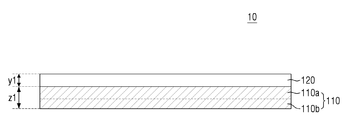
도 1은 본 발명의 일 실시예에 따른 보호 필름을 도시한 단면도이다.
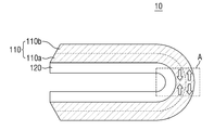
도 2는 도 1의 보호 필름이 접힌 모습을 도시한 단면도이다.
도 3은 도 1의 보호 필름이 유기발광 표시장치에 부착된 모습을 도시한 단면도이다.
도 4는 도 1의 보호 필름이 부착된 표시장치를 접는 모습을 도시한 단면도이다.
도 5는 도 1의 보호 필름이 부착된 표시장치를 펼치는 모습을 도시한 단면도이다.
도 6은 도 4 및 도 5의 과정이 반복되는 경우 A 영역에서 점착층의 변형에 따른 인장력의 양을 나타낸 그래프이다.
도 7은 기재층의 두께별로 점착층의 두께에 따른 점착층의 변형율을 나타낸 그래프이다.
도 8은 비교예로서, 최대 가용 두께를 초과한 점착층이 적용된 보호 필름을 접은 모습을 도시한 단면도이다.
도 9는 본 발명의 다른 실시예에 따른 보호 필름을 도시한 단면도이다.
도 10은 본 발명의 다른 실시예에 따른 보호 필름을 도시한 단면도이다.1 is a cross-sectional view showing a protective film according to an embodiment of the present invention.
2 is a cross-sectional view showing a state in which the protective film of FIG. 1 is folded.
3 is a cross-sectional view illustrating a state in which the protective film of FIG. 1 is attached to an organic light emitting display device.
4 is a cross-sectional view illustrating a state in which the display device to which the protective film of FIG. 1 is attached is folded.
5 is a cross-sectional view illustrating a state in which the display device to which the protective film of FIG. 1 is attached is unfolded.
6 is a graph showing the amount of tensile force according to the deformation of the adhesive layer in region A when the processes of FIGS. 4 and 5 are repeated.
7 is a graph showing the strain of the adhesive layer according to the thickness of the adhesive layer for each thickness of the base layer.
8 is a cross-sectional view showing a folded state of a protective film to which an adhesive layer exceeding a maximum usable thickness is applied as a comparative example.
9 is a cross-sectional view showing a protective film according to another embodiment of the present invention.
10 is a cross-sectional view showing a protective film according to another embodiment of the present invention.
본 발명의 이점 및 특징, 그리고 그것들을 달성하는 방법은 첨부되는 도면과 함께 상세하게 후술되어 있는 실시예들을 참조하면 명확해질 것이다. 그러나 본 발명은 이하에서 개시되는 실시예들에 한정되는 것이 아니라 서로 다른 다양한 형태로 구현될 것이며, 단지 본 실시예들은 본 발명의 개시가 완전하도록 하며, 본 발명이 속하는 기술분야에서 통상의 지식을 가진 자에게 발명의 범주를 완전하게 알려주기 위해 제공되는 것이며, 본 발명은 청구항의 범주에 의해 정의될 뿐이다. Advantages and features of the present invention, and methods for achieving them will be clarified with reference to embodiments described below in detail together with the accompanying drawings. However, the present invention is not limited to the embodiments disclosed below, but will be implemented in various different forms, and only the present embodiments allow the disclosure of the present invention to be complete, and the ordinary knowledge in the technical field to which the present invention pertains. It is provided to fully inform the holder of the scope of the invention, and the invention is only defined by the scope of the claims.
소자(elements) 또는 층이 다른 소자 또는 층의 "위(on)" 또는 "상(on)"으로 지칭되는 것은 다른 소자 또는 층의 바로 위뿐만 아니라 중간에 다른 층 또는 다른 소자를 개재한 경우를 모두 포함한다. 반면, 소자가 "직접 위(directly on)" 또는 "바로 위"로 지칭되는 것은 중간에 다른 소자 또는 층을 개재하지 않은 것을 나타낸다.Elements or layers referred to as "on" or "on" of another device or layer are not only directly above the other device or layer, but also when intervening another layer or other device in the middle. All inclusive. On the other hand, when a device is referred to as “directly on” or “directly above”, it indicates that no other device or layer is interposed therebetween.
전자 기기(electronic device)는 기기 본체만 제공될 수 있지만, 상기 본체의 표면을 적어도 일부분 감싸며 부착되면서 외부 충격으로부터 상기 본체가 손상되는 것을 방지하는 보호 필름을 부착한채로 제공되기도 한다. 상기 전자 기기는 예를 들면, 표시 패널이 포함된 전자 제품으로서 스마트폰, 태블릿 컴퓨터, 이동 전화기, 영상 전화기, 전자책 리더기, 데스크탑 컴퓨터, 랩탑 컴퓨터, 넷북 컴퓨터, 워크스테이션, 서버, PDA(personal digital assistant), PMP(portable multimedia player), MP3 플레이어, 모바일 의료기기, 카메라, 또는 웨어러블 장치(wearable device)중 하나일 수 있고, 또는 가전 제품으로서 텔레비전, DVD 플레이어(Digital Video Disk player), 오디오, 냉장고, 에어컨, 청소기, 오븐, 전자레인지, 세탁기, 공기 청정기, 셋톱 박스(set-top box), 홈 오토매이션 컨트롤 패널(home automation control panel), 보안 컨트롤 패널(security control panel), TV 박스, 게임 콘솔, 전자 사전, 전자 키, 캠코더, 또는 전자 액자중 하나일 수 있고, 의료기기(예: 각종 휴대용 의료측정기기(혈당 측정기, 심박 측정기, 혈압 측정기, 또는 체온 측정기 등), MRA(magnetic resonance angiography), MRI(magnetic resonance imaging), CT(computed tomography), 촬영기, 또는 초음파기 등), 네비게이션(navigation) 장치, 위성 항법 시스템(GNSS(Global Navigation Satellite System)), EDR(event data recorder), FDR(flight data recorder), 자동차 인포테인먼트(infotainment) 장치, 선박용 전자 장비(예: 선박용 항법 장치, 자이로 콤파스 등), 항공 전자기기(avionics), 보안 기기, 차량용 헤드 유닛(head unit), 산업용 또는 가정용 로봇, 금융 기관의 ATM(automatic teller's machine), 상점의 POS(point of sales), 또는 사물 인터넷 장치(internet of things)(예: 전구, 각종 센서, 전기 또는 가스 미터기, 스프링클러 장치, 화재경보기, 온도조절기(thermostat), 가로등, 토스터(toaster), 운동기구, 온수탱크, 히터, 보일러 등)중 하나일 수 있다.An electronic device may be provided with only the device body, but may also be provided with a protective film attached to at least partially cover the surface of the body and prevent the body from being damaged from external impact. The electronic device is, for example, an electronic product including a display panel, a smart phone, a tablet computer, a mobile phone, a video phone, an e-book reader, a desktop computer, a laptop computer, a netbook computer, a workstation, a server, and a personal digital (PDA). assistant), PMP (portable multimedia player), MP3 player, mobile medical device, camera, or wearable device (wearable device), or as a household appliance, television, DVD player (Digital Video Disk player), audio, refrigerator , Air conditioner, cleaner, oven, microwave, washing machine, air purifier, set-top box, home automation control panel, security control panel, TV box, game It can be one of a console, electronic dictionary, electronic key, camcorder, or electronic picture frame, and medical devices (eg, various portable medical measuring devices (blood glucose meter, heart rate meter, blood pressure side) Regular or body temperature meters, etc., magnetic resonance angiography (MRA), magnetic resonance imaging (MRI), computed tomography (CT), imaging, or ultrasound), navigation devices, satellite navigation systems (GNSS (Global Navigation Satellite) System)), EDR (event data recorder), FDR (flight data recorder), automotive infotainment devices, marine electronic equipment (e.g. marine navigation devices, gyro compasses, etc.), avionics, security devices, Head units for vehicles, industrial or household robots, automatic teller's machines (ATMs) in financial institutions, point of sales (POS) in stores, or Internet of things (eg light bulbs, various sensors, electricity) Or it may be one of a gas meter, a sprinkler device, a fire alarm, a thermostat, a street light, a toaster, exercise equipment, a hot water tank, a heater, a boiler, and the like.
다양한 실시 예에서, 전자 기기는 전술한 다양한 기기들 중 하나 또는 그 이상의 조합일 수 있다. 어떤 실시 예에 따른 전자 기기는 플렉서블 전자 기기 이거나 폴더블 전자 기기일 수 있다. In various embodiments, the electronic device may be a combination of one or more of the various devices described above. The electronic device according to an embodiment may be a flexible electronic device or a foldable electronic device.
본 명세서는 설명의 편의를 위해, 전자 기기의 일 예로서 폴더블 유기발광 표시장치(organic light emitting display device)에 대하여 설명한다.For convenience of description, this specification describes a foldable organic light emitting display device as an example of an electronic device.
폴더블 표시장치라 함은 패널의 형상과 관계없이 쉽게 접고 펴는 것이 반복 가능한 표시장치를 의미하거나, 또는 패널 자체가 쉽게 접고 펴는 것이 불가하더라도 두개 이상의 패널을 결합수단에 의해 결합하여 상기 결합 수단을 통해 접고 펴는 것이 가능한 표시장치를 의미할 수 있다.The foldable display device means a display device that can be easily folded and unfolded regardless of the shape of the panel, or even if the panel itself is not easily foldable and unfoldable, two or more panels can be combined by means of combining means through the combining means. It may mean a display device capable of folding and unfolding.
폴더블 표시장치는 상술한 유기발광 표시장치 이외에도 액정 표시장치(liquid crystal display device), 플라즈마 표시장치(plasma display device), 전기영동 표시장치(electrophoretic display device) 및 일렉트로웨팅 표시장치(electrowetting display device)를 포함할 수 있다.The foldable display device includes a liquid crystal display device, a plasma display device, an electrophoretic display device, and an electrowetting display device in addition to the organic light emitting display device described above. It may include.
본 문서의 실시 예에 따른 전자 기기는 유기발광 표시장치 및 전술한 기기들에 한정되지 않으며, 기술 발전에 따른 새로운 전자 기기를 포함할 수도 있다.The electronic device according to the exemplary embodiment of the present document is not limited to the organic light emitting display device and the aforementioned devices, and may include a new electronic device according to technological development.
이하, 첨부한 도면들을 참조하여, 본 발명의 실시예들을 보다 상세하게 설명하고자 한다. 도면상의 동일한 구성 요소에 대해서는 동일하거나 유사한 참조 부호를 사용한다. 도면에서 여러 층 및 영역을 명확하게 표현하기 위하여 두께를 확대하여 나타내었다. 그리고 도면에서, 설명의 편의를 위해, 일부 층 및 영역의 두께를 과장되게 나타내었다.Hereinafter, embodiments of the present invention will be described in detail with reference to the accompanying drawings. The same or similar reference numerals are used for the same elements in the drawings. In the drawings, thicknesses are enlarged to clearly represent various layers and regions. In the drawings, thicknesses of some layers and regions are exaggerated for convenience of description.
도 1은 본 발명의 일 실시예에 따른 보호 필름을 도시한 단면도이고, 도 2는 도 1의 보호 필름이 접힌 모습을 도시한 단면도이고, 도 3은 도 1의 보호 필름이 유기발광 표시장치에 부착된 모습을 도시한 단면도이다.1 is a cross-sectional view showing a protective film according to an embodiment of the present invention, Figure 2 is a cross-sectional view showing a folded state of the protective film of Figure 1, Figure 3 is a protective film of Figure 1 is an organic light emitting display device It is a sectional view showing the attached state.
도 1 내지 도 3을 참조하면, 보호 필름(10)은 유기발광 표시장치(20)의 일 면 상에 부착된다. 도면에 도시되진 않았지만, 보호 필름(10)은 유기발광 표시장치(20)의 일 면뿐만 아니라 상기 일 면의 측면 에지를 포함하여 상기 유기발광 표시장치(20)의 일부를 감싸도록 부착될 수도 있다. 보호 필름(10)은 기재층(120) 및 기재층(120)의 일면 상에 배치되는 점착층(110)을 포함한다.1 to 3, the
기재층(120)은 보호 필름(10)이 유기발광 표시장치(20)에 부착된 경우, 실질적으로 유기발광 표시장치(20)를 보호하는 층일 수 있다. 기재층(120)은 PET(Polyethylene terephthalate), PEN(Polyethylene naphthalate), PC(poly carbonate), PMMA(Polymethylmetacrylate), 폴리스티렌(Polystyrene), 폴리염화비닐(Polyvinylchloride), PES(Polyethersulfone), 폴리 에틸렌, 폴리 프로필렌, TRF 필름 및 이들의 조합으로 이루어진 군에서 선택된 적어도 하나를 포함할 수 있다.The
기재층(120)의 두께는 약 20㎛ 이상일 수 있다. 일 실시예에서, 기재층(120)의 두께는 약 25㎛ 내지 약 75㎛일 수 있으며, 상기 범위 내의 두께를 가짐으로써 보호 필름(10)의 총 두께를 지나치게 증가시키지 않으면서 유기발광 표시장치(20)의 표면을 충분히 보호할 수 있다.The thickness of the
점착층(110)은 및 기재층(120)의 일면 상에 배치된다. 점착층(110)은 일면에 유기발광 표시장치(20)에 부착되도록 하는 접착면을 구비할 수 있다. 점착층(110)의 타면은 기재층(120)의 상기 일면과 접할 수 있다. 보호 필름(10)이 유기발광 표시장치(20)에 부착된 경우, 점착층(110)은 유기발광 표시장치(20)에 직접 접할 수 있다. 점착층(110)은 기재층(120)과 유기발광 표시장치(20) 사이에서 기재층(120)이 유기발광 표시장치(20)에 부착되도록 접착하는 기능을 포함한다. 점착층(110)은 아크릴 계열 접착제, 실리콘 계열 접착제, 우레탄 계열 접착제, 고무 계열 접착제, 비닐 에테르 계열 접착제 등을 포함하는 OCA 접착제, PSA 접착제 등을 사용하여 형성될 수 있다. 점착층(110)은 일 실시예에서 -20°C 이하의 온도에서 10MPa이하의 모듈러스(modulus)를 갖는 PSA 접착제로 구성될 수 있다.The
점착층(110)은 보호 필름(10)을 구부릴 경우, 보호 필름(10) 내부에 압축력이 발생되는 제1 영역(110a)과 인장력이 발생되는 제2 영역(110b)을 포함할 수 있다. 예를 들어 유기발광 표시장치(20)의 발광면의 표면에 보호 필름(10)이 부착되고, 보호 필름(10)이 부착된 유기발광 표시장치(20)를 발광면이 안쪽을 향하도록 구부린 경우, 점착층(110) 내 기재층(120)과 상대적으로 가까운 영역인 제1 영역(110a)에서 압축력이 발생되고 점착층(110) 내 유기발광 표시장치(20)와 상대적으로 가까운 영역인 제2 영역(110b)에서 인장력이 발생될 수 있다.When the
도면에서, 점착층(110) 내 인장력과 압축력이 발생되는 경계가 점착층(110)이 기재층(120)과 접촉하는 표면과 점착층(110)이 유기발광 표시장치(20)와 접촉하는 표면의 중간지점인 것으로 도시되었으나, 이에 한정되는 것은 아니다. 점착층의 재질에 따라 인장력과 압축력이 발생되는 경계가 상대적으로 점착층(110)이 기재층(120)과 접촉하는 표면보다 점착층(110)이 유기발광 표시장치(20)와 접촉하는 표면에 가까운 위치에 형성될 수도 있고, 상대적으로 점착층(110)이 유기발광 표시장치(20)와 접촉하는 표면 보다 점착층(110)이 기재층(120)과 접촉하는 표면에 가까운 위치에 형성될 수도 있다. 즉, 점착층(110) 내 제1 영역(110a)과 제2 영역(110b)의 두께는 같을 수도 있고, 상대적으로 제1 영역(110a)의 두께가 제2 영역(110b)의 두께보다 두꺼울 수 있고, 상대적으로 제2 영역(110b)의 두께가 제1 영역(110a)의 두께보다 두꺼울 수도 있다.In the drawing, the surface where the
제1 영역(110a)에서 압축력의 크기는 위치마다 다를 수 있다. 제1 영역(110a)에서 상대적으로 구부러지는 영역(예를 들면, A영역)에 가까울수록 압축력의 크기는 커질 수 있다. 마찬가지로, 제2 영역(110b)에서 인장력의 크기는 위치마다 다를 수 있다. 제2 영역(110b)에서 상대적으로 구부러지는 영역에 가까울수록 압축력의 크기는 커질 수 있다.The size of the compressive force in the
도 2와 같이 제2 영역(110b)의 곡률 반경이 제1 영역(110a)의 곡률 반경보다 크도록 외력을 가해 보호 필름(10)을 구부린 경우, 제1 영역(110a)은 외부에서 인장력이 작용될 수 있고, 제2 영역(110b)은 외부에서 압축력이 작용될 수 있다. 따라서, 도 2와 같이 보호 필름(10)을 구부린 경우, 점착층(110)의 측면은 경사진 모습일 수 있다. 즉, 도 2와 같이 보호 필름(10)을 구부린 경우, 외력에 의해, 점착층(110)은 제1 영역(110a)에서 제2 영역(110b)으로 갈수록 길이가 줄어들 수 있다. 이 때, 점착층(110)은 복원되려는 힘이 점착층(110) 내부에 발생하게 되므로 외력이 가해지기 전보다 길이가 늘어난 제1 영역(110a)은 내부에 압축력이 발생할 수 있고, 외력이 가해지기 전보다 길이가 짧아진 제2 영역(110b)은 내부에 인장력이 발생할 수 있다.When the
본 실시예에 따른 보호 필름(10)의 점착층(110)은 최대 가용 두께 이하의 두께를 가지고 있으므로, 1000회 이상 보호 필름(10)을 접고 펴는 것을 반복하여도 버클링(buckling)되는 현상이 발생되지 않을 수 있다. 점착층(110)의 최대 가용 두께에 대해서는 상세히 후술된다.Since the
일 구현예에서, 보호 필름(10)은 예를 들어, 광투과율이 약 90% 이상이고, 헤이즈가 약 1% 이하일 수 있고, 구체적으로는 광투과율이 약 91% 내지 약 95%이고, 헤이즈가 약 0.5%이고 약 0.8%일 수 있다. 상기 범위 내의 광투과율 및 헤이즈를 가짐으로써 우수한 광학 물성을 구현할 수 있다. 상기 광투과율은 ISO13468의 조건에 따라 측정하고, 상기 헤이즈는 ISO14782의 조건에 따라 측정한 값을 의미할 수 있다.In one embodiment, the
또한, 보호 필름(10)은 ASTM D638의 조건에 따른 기재층(120)의 모듈러스가 약 2GPa 내지 약 9GPa일 수 있다. 상기 범위 내의 모듈러스를 가짐으로써 충분한 내구성 및 우수한 유연성을 동시에 구현할 수 있다. 기재층(120)은 일 실시예에서 약 -40°C 내지 약 80°C의 온도 조건에서도 약 2GPa 내지 약 9GPa의 모듈러스를 갖을 수 있다.In addition, the
구체적으로 기재층(120)의 모듈러스가 약 2GPa 미만인 경우 필름의 영구 변형이 용이하게 일어날 수 있고, 약 9GPa 초과인 경우 굽힘 등에 따른 필름의 균열 또는 크랙이 용이하게 발생할 수 있는 문제가 있다.Specifically, when the modulus of the
전술한 바와 같이, 보호 필름(10)은 우수한 광학 물성, 충분한 내구성 및 우수한 유연성을 가질 수 있고, 이와 동시에 상기 유기발광 표시장치(20)의 기판(210), 예를 들어 투명 플라스틱 재질의 기판의 표면에 적용되어 사용되는 경우라도 더욱 향상된 유연성에 의해 깨짐 또는 명점 현상이 방지되면서 외부의 자극, 마찰 등에 저항하는 탄성력에 의해 표면에 스크래치 등이 일시적으로 발생하더라도 시간이 지남에 따라 본래의 표면 형상으로 복원될 수 있다.As described above, the
그 결과, 보호 필름(10)은 계속적인 사용에도 불구하고 이의 물성이 쉽게 저하되지 않아, 우수한 광학 물성 및 우수한 내구성을 장기간 구현할 수 있다.As a result, the
유기발광 표시장치(20)에 적용되는 보호 필름(10)에서 기재층(120)이 일 두께(y1)를 가진 경우, 점착층(110)의 최대 가용 두께는 z1일 수 있다. 기재층(120)의 두께와 점착층(110)의 두께에 대한 설명은 기재층(120)의 모듈러스의 관계에 대한 설명과 함께 상세히 후술된다.When the
다음으로 보호 필름(10)이 부착될 수 있는 유기발광 표시장치(20)에 대해 설명한다. Next, the organic light emitting
도 3을 참조하면, 유기발광 표시장치(20)는 기판(210), 기판(210) 상에 배치되는 유기발광소자층(220), 유기발광소자층(220) 상에 배치되는 봉지막(230), 봉지막(230) 상에 배치되는 터치감지층(240) 및 터치감지층(240) 상에 배치되는 커버 윈도우(250)를 포함할 수 있다.Referring to FIG. 3, the organic light emitting
기판(210)은 플랙서블 표시 기판일 수 있다. 상기 플렉서블 표시 기판은 휘거나 접힐 수 있는 유연한 소재로 이루어진 것을 특징으로 한다. 예를 들어, 플렉서블 표시 기판은 폴리이미드 필름과 같은 플라스틱 필름으로 이루어지거나, 박판 유리, 박막의 금속 필름 등으로 이루어질 수 있다. 기판(210)은 이에 제한되지 않고 리지드 표시 기판 또는 플랙서블 표시 기판일 수도 있다.The
유기발광소자층(220)은 기판(210) 상에 배치된다. 도시되진 않았지만, 기판(210)과 유기발광소자층(220) 사이에 기판(210)의 상면을 평활하게 하며 유기발광소자층(220)으로 불순물의 침투를 차단하는 버퍼막(buffer layer)이 배치될 수도 있다.The organic light emitting
유기발광소자층(220)은 복수의 박막 트랜지스터 및 유기발광 다이오드(OLED)를 포함할 수 있다. 상기 유기발광 다이오드는 애노드 전극, 유기 발광층 및 캐소드 전극이 차례로 적층된 구조일 수 있다. 상기 복수의 박막 트랜지스터 중 일부 박막 트랜지스터의 소스/드레인 전극과 상기 유기발광 다이오드의 애노드 전극이 전기적으로 연결될 수 있다.The organic light emitting
봉지막(230)은 유기발광소자층(220)을 덮도록 기판(210)의 전체 면에 걸쳐 형성된다. 봉지막(230)은 외부의 수분이나 산소 등으로부터 유기발광 다이오드를 보호하기 위해 형성된다. 봉지막(230)은 절연성 무기 물질로 이루어진 막이 다층 또는 단층으로 이루어질 수 있다. 예컨대 무기 물질은 금속 산화물 또는 금속 질화물일 수 있으며, 구체적으로 무기 물질은 실리콘산화물(SiO2), 실리콘질화물(SiNx), 실리콘산질화물(SiON), 알루미늄산화물(Al2O3), 티타늄산화물(TiO2), 탄탈산화물(Ta2O5), 하프늄산화물(HfO2), 또는 아연산화물(ZrO2) 등을 포함할 수 있다. 한편, 봉지막(230)은 절연성 무기 물질로 이루어진 막 상에 유기 물질로 이루어진 박막 및 무기 물질로 이루어진 박막이 교대로 더 적층되어 봉지 구조를 이룰 수 있다.The
이와 같이 본 발명의 일 실시예에 의하면, 유연성 있는 플렉서블 표시 기판(210)과 박막으로 형성되어 유연성이 있는 봉지막(230)을 채용함으로써, 표시장치(20)를 구부리거나, 접거나, 펼침이 가능하게 되는 것이다.As described above, according to an embodiment of the present invention, the
봉지막(230) 상에 터치감지층(240)이 배치될 수 있다. 터치감지층(240)은 일 실시예에서 정전 용량 타입(electrostatic capacitive type)의 터치 스크린 패널이 적용될 수 있다. 다만, 이에 제한되는 것은 아니고 터치감지층(240)은 저항막 타입(resistive type)이나, 전자기장 타입(electro-magnetic type)이나, 소오 타입(surface acoustic wave type, saw type)이나, 인프라레드 타입(infrared type)중 선택되는 어느 하나의 터치 스크린 패널이 적용될 수도 있다. 터치감지층(240)은 플렉서블 표시 기판(210)과 마찬가지고 구부리거나 접힐 수 있는 유연한 소재를 사용한다. 다른 실시예에서, 터치감지층(240)은 생략될 수도 있다.The
커버 윈도우(250)는 터치감지층(240) 상에 배치된다. 도시되진 않았지만, 커버 윈도우(250)는 커버 윈도우(250)와 터치감지층(240) 사이에 배치되는 광학적 투명 접착제(Optically Clear Adhesive, OCA) 또는 광학적 투명 수지(Optically Clear Resin, OCR)를 사용하여 터치감지층(240)에 접착될 수 있다.The
커버 윈도우(250)는 높은 모듈러스를 갖는 유리를 포함할 수 있다. 상기 커버 윈도우(250)의 모듈러스는 일 실시예에서 약 50GPa 이상일 수 있다. 높은 모듈러스를 갖는 커버 윈도우(250)는 커버 윈도우(250)에 부착된 보호 필름(10)의 점착층(110)이 두꺼워 지더라도 쉽게 버클링이 발생하지 않도록 도움을 줄 수 있다.The
커버 윈도우(250)는 크랙, 흠과 같은 손상으로부터 보호되기 위하여, 윈도우 필름(251) 및 윈도우 필름(251)의 표면에 형성되어 윈도우 필름(251)의 손상 발생 확률을 낮추기 위한 코팅층(252)을 포함할 수 있다. 윈도우 필름(251)은 투명한 플라스틱 필름으로 이루어질 수 있다. 상기 플라스틱 필름은 예시적으로 폴리에틸렌테레프탈레이트, 폴리메틸메타크릴레이트, 폴리카보네이트 및 폴리이미드 등을 포함할 수 있지만, 상술한 바에 한정되는 것은 아니다.The
다른 실시예에서, 커버 윈도우(250)의 소재는 상기 유리에 제한되지 않고, 다른 실시예에서 유기발광 표시장치(20)의 구부림, 접고 펼침이 가능하도록 유연한 소재를 포함할 수도 있다.In another embodiment, the material of the
유기발광소자층(220)에서 발광되는 빛이 커버 윈도우(250)를 통해 사용자에게 시인될 수 있다. 보호 필름(10)은 발광면인 커버 윈도우(250) 상에 부착될 수 있다.Light emitted from the organic light emitting
상술한 유기발광 표시장치(20)의 커버 윈도우(250)는 코팅층(252)을 포함하더라도 외부 충격에 쉽게 손상을 받을 수 있다. 따라서, 보호 필름(10)을 커버 윈도우(250) 상에 부착하여 유기발광 표시장치(20)를 외부 충격에 의해 쉽게 손상되는 것을 방지할 수 있다.The
다음으로, 기재층(120)과 점착층(110)의 결합관계에 대해 설명한다.Next, the bonding relationship between the
도 4는 도 1의 보호 필름이 부착된 표시장치를 접는 모습을 도시한 단면도이고, 도 5는 도 1의 보호 필름이 부착된 표시장치를 펼치는 모습을 도시한 단면도이고, 도 6은 도 4 및 도 5의 과정이 반복되는 경우 A 영역에서 점착층의 변형에 따른 인장력의 양을 나타낸 그래프이고, 도 7은 기재층의 두께별로 점착층의 두께에 따른 점착층의 변형율을 나타낸 그래프이고, 도 8은 비교예로서, 최대 가용 두께를 초과한 점착층이 적용된 보호 필름을 접은 모습을 도시한 단면도이다.4 is a cross-sectional view showing a state in which the display device with the protective film of FIG. 1 is folded, FIG. 5 is a cross-sectional view showing a state in which the display device with the protective film of FIG. 1 is unfolded, and FIG. When the process of FIG. 5 is repeated, it is a graph showing the amount of tensile force due to the deformation of the adhesive layer in the area A, and FIG. 7 is a graph showing the strain of the adhesive layer according to the thickness of the adhesive layer for each thickness of the base layer, and FIG. 8 As a comparative example, it is a cross-sectional view showing a state in which a protective film to which an adhesive layer exceeding a maximum usable thickness is applied is folded.
도 4 및 도 5를 참조하면, 상술한 것과 같이, 유기발광 표시장치(20)는 폴더블 표시장치(20)이고, 본 발명의 일 실시예에 따른 보호 필름(10)이 상기 폴더블 표시장치(20) 상에 부착될 수 있다. 유기발광 표시장치(20)는 A영역에서 접고 펼침이 가능할 수 있다. 유기발광 표시장치(20)가 A영역에서 접고 펼쳐지는 경우, 유기발광 표시장치(20) 상에 부착된 보호 필름(10)은 유기발광 표시장치(20)와 마찬가지로 A영역에서 접고 펼쳐질 수 있다.4 and 5, as described above, the organic light emitting
유기발광 표시장치(20)가 접히는 방향은 발광면이 안쪽을 향하는 방향일 수 있다. 즉, 유기발광 표시장치(20)의 커버 윈도우(250) 상에 보호 필름(10)이 부착된 경우, 기재층(120), 점착층(110), 커버 윈도우(250), 기판(210)의 순서대로 A영역에서 곡률 반경이 커지도록 접힐 수 있다.The direction in which the organic light emitting
보호 필름(10)이 최대로 접힌 경우, 기재층(120)의 곡률 반경은 약 0.5R 이상일 수 있다. 일 실시예에서, 기재층(120)의 곡률 반경은 약 0.5R 내지 약 1.5R일 수 있다. 여기서, 기재층(120)의 곡률 반경이라 함은 기재층(120)과 점착층(110)이 접착된 접착면의 곡률 반경일 수 있다.When the
보호 필름(10)이 최대로 접힌 경우, 점착층(110) 내부에 존재하는 인장력과 압축력으로 인하여, 점착층(110)의 측면은 경사질 수 있다. 이 경우, 점착층(110)의 곡률 반경이 0.5R 이상인 조건에서 기재층(120)의 일 측면의 접선과 점착층(110)의 경사면이 이루는 각도(θ)는 2° 이상일 수 있다. 일 실시예에서, 상기 각도(θ)는 3° 내지 25°일 수 있다.When the
도 6을 참조하면, 도시된 그래프는 제1 실험예로서, 도 4와 같이 보호 필름(10)이 부착된 표시장치(20)를 접고 펼침을 반복하는 경우, 점착층(110) 내 인장력과 점착층(110)의 인장 변형율을 나타낸 그래프이다. 여기서 인장 변형율은 인장 하중을 가했을 때의 늘어난 길이와 원래의 길이와의 비율을 의미한다.Referring to FIG. 6, the illustrated graph is a first experimental example. When folding and unfolding the
도 6의 실선 그래프(cyclic test)를 참조하면, 보호 필름(10)에 힘이 가해지지 않는 경우(도 3처럼 보호 필름(10)이 평평하게 부착된 경우)는 점착층(110)에 가해지는 인장력은 0MPa에 가까울 수 있다. 보호 필름(10)이 도 4처럼 외력이 가해져 접혀지기 시작하는 경우, 인장 변형율이 증가하고, 점착층(110)의 인장력은 증가할 수 있다. 보호 필름(10)이 도 5처럼 외력이 가해져 펼쳐지기 시작하는 경우, 인장 변형율이 증가하고, 점착층(110)의 인장력은 감소할 수 있다. 도 5의 경우, 인장 변형율이 감소하는 것은 보호 필름(10)이 펼쳐 지면서 원래 형상으로 돌아오게 되고, 그 때 점착층(110)의 형상이 일부 복원되므로 인장력의 감소와 함께 인장 변형율이 일부 감소하게 된다. 다만, 도 5의 경우, 복원 임계점을 넘는 변형이 일어나 점착 층의 인장 변형율이 0%로 복원되지는 않을 수 있다. 도면에 도시되지는 않았지만, 보호 필름(10)의 접고 펼침이 반복되는 경우, 인장 변형율을 최대 인장 변형율에 가까워질 수 있다.Referring to the solid line graph (cyclic test) of FIG. 6, when no force is applied to the protective film 10 (when the
여기서, 보호 필름(10)이 상기 최대 인장 변형율을 넘기게 되면, 점착층(110)은 버클링이 일어나게 될 수 있다. Here, when the
도 6의 점선 그래프(tensile test)를 참조하면, 보호 필름(10)을 한 번 접고 펼치는 과정을 한 사이클이라고 하면, 사이클당 최대 인장력이 존재할 수 있다. 보호 필름(10)은 보호 필름(10)이 최대로 접힌 경우 상기 사이클당 최대 인장력을 포함하게 될 수 있다. 상기 사이클당 최대 인장력은 약 200MPa가 될 때까지 급격히 증가하되, 200MPa 이상부터 서서히 증가하게 될 수 있다. 즉, 사이클당 최대 인장력은 200MPa 전후로 변화율이 감소될 수 있다.Referring to the dotted line graph (tensile test) of FIG. 6, if the process of folding and unfolding the
도 6은 보호 필름(10)이 접고 펼치는 과정이 반복되는 경우, 보호 필름(10)의 인장 변형율 및 보호 필름(10) 내 인장력에 대한 개형을 설명하기 위한 예시적인 그래프이다. 보호 필름(10)의 인장 변형율 및 보호 필름(10) 내 인장력은 모든 실험예에서 본 그래프가 지시하는 값에 제한되는 것은 아니다. 다른 실시예에서, 보호 필름(10) 내 인장력의 인장 변형율이 약 200MPa 값이 아닌 다른 값을 전후로 변화율이 감소될 수도 있고, 보호 필름(10)의 인장 변형율은 도 6과 달리 더 큰 변화율로 증가, 감소하거나 더 작은 변화율로 증가, 감소할 수 있다. 6 is an exemplary graph for explaining the deformation of the tensile strain in the
도 7을 참조하면, 여러 실험을 통해 기재층(120)의 곡률반경이 1.5R인 경우 약 65°C의 고온 조건에서 기재층(120)의 모듈러스 및 두께에 따라 가용될 수 있는 점착층(110)의 두께 및 점착층(110)의 최대 압축 변형을 알아 보았다. 도 7에 따른 실험 결과 그래프는 도 4 및 도 6와 같이 보호 필름(10)이 부착된 표시장치(20)를 접고 펼침을 1000회 이상 반복한 후 점착층(110)의 최대 압축 변형율을 나타내었다. 압축 변형율은 외부의 압축력에 따른 변형율로서, 도 6의 인장 변형율과 반대 부호를 갖을 수 있다. 실험자는 실험을 통해 기재층(120)에 약 25μm, 약 35μm, 약 50μm, 약 75μm, 및 약 100μm의 두께를 가지는 점착층(110)을 부착해 점착층(110)의 최대 압축 변형율 및 점착층(110)의 버클링 여부를 알아보았다. 도 7의 그래프에서 가로축의 값은 점착층(110)의 두께를 나타내고, 세로축은 점착층(110)의 최대 압축 변형율을 나타낸다. 이하, 최대 압축 변형율은 설명의 편의를 위해 절대값을 기준으로 설명한다.Referring to FIG. 7, when the curvature radius of the
제2 실험예에 따른 보호 필름(10_2)은 두께가 약 25μm이고, 모듈러스가 약 4.15GPa인 기재층(120)을 포함한다. 제2 실험예를 참조하면, 점착층(110)의 두께가 증가할수록 점착층(110)의 최대 압축 변형율은 점착층(110)의 두께 25μm에서 약 0.51%부터 증가하는 개형을 나타낸다. 다만, 점착층(110)의 두께가 약 75μm 및 약 100μm인 경우, 점착층(110)은 버클링이 발생하게 되었다.The protective film 10_2 according to the second experimental example includes a
제3 실험예에 따른 보호 필름(10_3)은 두께가 약 35μm이고, 모듈러스가 약 4.15GPa인 기재층(120)을 포함한다. 제3 실험예를 참조하면, 점착층(110)의 두께가 증가할수록 점착층(110)의 최대 압축 변형율은 점착층(110)의 두께 25μm에서 약 0.50%부터 증가하는 개형을 나타낸다. 다만, 제3 실험예는 제2 실험예 대비, 점착층(110)의 최대 압축 변형율이 각 점착층(110)의 두께에서 더 작은 값을 갖는다. 점착층(110)의 두께가 약 75μm 및 약 100μm인 경우, 점착층(110)은 버클링이 발생하게 되었다.The protective film 10_3 according to the third experimental example includes a
제4 실험예에 따른 보호 필름(10_4)은 두께가 약 40μm이고, 모듈러스가 약 4.15GPa인 기재층(120)을 포함한다. 제4 실험예를 참조하면, 점착층(110)의 두께가 증가할수록 점착층(110)의 최대 압축 변형율은 점착층(110)의 두께 25μm에서 약 0.49%부터 증가하는 개형을 나타낸다. 다만, 제4 실험예는 제3 실험예 대비, 점착층(110)의 최대 압축 변형율이 각 점착층(110)의 두께에서 더 작은 값을 갖는다. 점착층(110)의 두께가 약 100 μm인 경우, 점착층(110)은 버클링이 발생하게 되었다.The protective film 10_4 according to the fourth experimental example includes a
제5 실험예에 따른 보호 필름(10_5)은 두께가 약 50μm이고, 모듈러스가 약 4.15GPa인 기재층(120)을 포함한다. 제5 실험예를 참조하면, 점착층(110)의 두께가 증가할수록 점착층(110)의 최대 압축 변형율은 점착층(110)의 두께 25μm에서 약 0.49%부터 감소하다가 다시 증가하는 개형을 나타낸다. 다만, 제5 실험예는 제4 실험예 대비, 점착층(110)의 최대 압축 변형율이 각 점착층(110)의 두께에서 더 작은 값을 갖는다. 점착층(110)의 두께가 약 25μm, 약 35μm, 약 50μm, 약 75μm, 및 약 100μm인 경우 모두 버클링이 발생되지 않았다.The protective film 10_5 according to the fifth experimental example includes a
제6 실험예에 따른 보호 필름(10_6)은 두께가 약 65μm이고, 모듈러스가 약 4.15GPa인 기재층(120)을 포함한다. 제6 실험예를 참조하면, 점착층(110)의 두께가 증가할수록 점착층(110)의 최대 압축 변형율은 점착층(110)의 두께 25μm에서 약 0.50%부터 감소하다가 다시 증가하는 개형을 나타낸다. 다만, 제6 실험예는 제5 실험예 대비, 점착층(110)의 최대 압축 변형율이 각 점착층(110)의 두께에서 항상 작은 값을 갖는 것은 아니고, 일부 낮은 두께의 점착층(110)의 경우 더 높은 최대 압축 변형율을 갖는다. 점착층(110)의 두께가 약 25μm, 약 35μm, 약 50μm, 약 75μm, 및 약 100μm인 경우 모두 버클링이 발생되지 않았다.The protective film 10_6 according to the sixth experimental example includes a
제7 실험예에 따른 보호 필름(10_7)은 두께가 약 75μm이고, 모듈러스가 약 4.15GPa인 기재층(120)을 포함한다. 제7 실험예를 참조하면, 점착층(110)의 두께가 증가할수록 점착층(110)의 최대 압축 변형율은 점착층(110)의 두께 25μm에서 약 0.51%부터 감소하다가 다시 증가하는 개형을 나타낸다. 다만, 제7 실험예는 제6 실험예 대비, 점착층(110)의 최대 압축 변형율이 각 점착층(110)의 두께에서 항상 작은 값을 갖는 것은 아니고, 일부 낮은 두께의 점착층(110)의 경우 더 높은 최대 압축 변형율을 갖는다. 점착층(110)의 두께가 약 25μm, 약 35μm, 약 50μm, 약 75μm, 및 약 100μm인 경우 모두 버클링이 발생되지 않았다.The protective film 10_7 according to the seventh experimental example includes a
제8 실험예에 따른 보호 필름(10_8)은 두께가 약 25μm이고, 모듈러스가 약 6.0GPa인 기재층(120)을 포함한다. 제8 실험예를 참조하면, 점착층(110)의 두께가 증가할수록 점착층(110)의 최대 압축 변형율은 점착층(110)의 두께 25μm에서 약 0.445%부터 증가하는 개형을 나타낸다. 다만, 제8 실험예는 제7 실험예 대비, 점착층(110)의 최대 압축 변형율이 각 점착층(110)의 두께에서 더 작은 값을 갖는다. 다만, 점착층(110)의 두께가 약 75μm 및 약 100μm인 경우, 점착층(110)은 버클링이 발생하게 되었다.The protective film 10_8 according to the eighth experimental example includes a
제9 실험예에 따른 보호 필름(10_9)은 두께가 약 35μm이고, 모듈러스가 약 6.0GPa인 기재층(120)을 포함한다. 제9 실험예를 참조하면, 점착층(110)의 두께가 증가할수록 점착층(110)의 최대 압축 변형율은 점착층(110)의 두께 25μm에서 약 0.44%부터 증가하는 개형을 나타낸다. 다만, 제9 실험예는 제8 실험예 대비, 점착층(110)의 최대 압축 변형율이 각 점착층(110)의 두께에서 더 작은 값을 갖는다. 다만, 점착층(110)의 두께가 약 75μm 및 약 100μm인 경우, 점착층(110)은 버클링이 발생하게 되었다.The protective film 10_9 according to the ninth experimental example includes a
제10 실험예에 따른 보호 필름(10_10)은 두께가 약 40μm이고, 모듈러스가 약 6.0GPa인 기재층(120)을 포함한다. 제10 실험예를 참조하면, 점착층(110)의 두께가 증가할수록 점착층(110)의 최대 압축 변형율은 점착층(110)의 두께 25μm에서 약 0.43%부터 감소하다가 다시 증가하는 개형을 나타낸다. 다만, 제10 실험예는 제9 실험예 대비, 점착층(110)의 최대 압축 변형율이 각 점착층(110)의 두께에서 더 작은 값을 갖는다. 점착층(110)의 두께가 약 25μm, 약 35μm, 약 50μm, 약 75μm, 및 약 100μm인 경우 모두 버클링이 발생되지 않았다.The protective film 10_10 according to the tenth experimental example includes a
제11 실험예에 따른 보호 필름(10_11)은 두께가 약 50μm이고, 모듈러스가 약 6.0GPa인 기재층(120)을 포함한다. 제11 실험예를 참조하면, 점착층(110)의 두께가 증가할수록 점착층(110)의 최대 압축 변형율은 점착층(110)의 두께 25μm에서 약 0.43%부터 감소하다가 다시 증가하는 개형을 나타낸다. 다만, 제11 실험예는 제10 실험예 대비, 점착층(110)의 최대 압축 변형율이 각 점착층(110)의 두께에서 더 작은 값을 갖는다. 점착층(110)의 두께가 약 25μm, 약 35μm, 약 50μm, 약 75μm, 및 약 100μm인 경우 모두 버클링이 발생되지 않았다.The protective film 10_11 according to the eleventh experimental example includes a
제12 실험예에 따른 보호 필름(10_12)은 두께가 약 65μm이고, 모듈러스가 약 6.0GPa인 기재층(120)을 포함한다. 제12 실험예를 참조하면, 점착층(110)의 두께가 증가할수록 점착층(110)의 최대 압축 변형율은 점착층(110)의 두께 25μm에서 약 0.44%부터 감소하다가 다시 증가하는 개형을 나타낸다. 다만, 제12 실험예는 제11 실험예 대비, 점착층(110)의 최대 압축 변형율이 각 점착층(110)의 두께에서 항상 작은 값을 갖는 것은 아니고, 일부 낮은 두께의 점착층(110)의 경우 더 높은 최대 압축 변형율을 갖는다. 점착층(110)의 두께가 약 25μm, 약 35μm, 약 50μm, 약 75μm, 및 약 100μm인 경우 모두 버클링이 발생되지 않았다.The protective film 10_12 according to the twelfth experimental example includes a
제13 실험예에 따른 보호 필름(10_13)은 두께가 약 25μm이고, 모듈러스가 약 9.0GPa인 기재층(120)을 포함한다. 제13 실험예를 참조하면, 점착층(110)의 두께가 증가할수록 점착층(110)의 최대 압축 변형율은 점착층(110)의 두께 25μm에서 약 0.38%부터 증가하는 개형을 나타낸다. 제13 실험예는 제12 실험예 대비, 점착층(110)의 최대 압축 변형율이 각 점착층(110)의 두께에서 더 작은 값을 갖는다. 다만, 점착층(110)의 두께가 약 75μm 및 약 100μm인 경우, 점착층(110)은 버클링이 발생하게 되었다.The protective film 10_13 according to the thirteenth experimental example includes a
제14 실험예에 따른 보호 필름(10_14)은 두께가 약 35μm이고, 모듈러스가 약 9.0GPa인 기재층(120)을 포함한다. 제14 실험예를 참조하면, 점착층(110)의 두께가 증가할수록 점착층(110)의 최대 압축 변형율은 점착층(110)의 두께 25μm에서 약 0.37%부터 증가하는 개형을 나타낸다. 제14 실험예는 제13 실험예 대비, 점착층(110)의 최대 압축 변형율이 각 점착층(110)의 두께에서 더 작은 값을 갖는다. 다만, 점착층(110)의 두께가 약 100μm인 경우, 점착층(110)은 버클링이 발생하게 되었다.The protective film 10_14 according to the 14th experimental example includes a
제15 실험예에 따른 보호 필름(10_15)은 두께가 약 40μm이고, 모듈러스가 약 9.0GPa인 기재층(120)을 포함한다. 제15 실험예를 참조하면, 점착층(110)의 두께가 증가할수록 점착층(110)의 최대 압축 변형율은 점착층(110)의 두께 25μm에서 약 0.36%부터 감소하다가 다시 증가하는 개형을 나타낸다. 제15 실험예는 제14 실험예 대비, 점착층(110)의 최대 압축 변형율이 각 점착층(110)의 두께에서 더 작은 값을 갖는다. 점착층(110)의 두께가 약 25μm, 약 35μm, 약 50μm, 약 75μm, 및 약 100μm인 경우 모두 버클링이 발생되지 않았다.The protective film 10_15 according to the fifteenth experimental example includes a
상기 실험예 이외에도 다른 여러 실험을 통해, 대략적으로 기재층(120)의 모듈러스가 증가할수록 점착층(110)의 최대 압축 변형율은 감소하고, 대략적으로 점착층(110)의 두께가 감소수록 점착층(110)의 최대 압축 변형율은 감소함을 알 수 있다. In addition to the above experimental examples, through various other experiments, the maximum compressive strain of the
기재층(120)의 모듈러스 및 기재층(120)의 두께에 따른 최대 가용할 수 있는 점착층(110)의 두께의 관계를 알아보기 위해 실험을 실시 하였다. 실험은 상술한 실험예와 마찬가지로 기재층(120)의 곡률반경이 1.5R인 경우 약 65°C의 고온 조건에서 측정한 값들이고, 그에 따른 실험 결과는 아래의 표 1과 같다. 표 1의 값은 대략적인 값으로, 일부 미세한 오차가 존재할 수 있다.An experiment was conducted to find out the relationship between the modulus of the
y[μm]Thickness of the base layer,
y [μm]
x[GPa]=4.15인 경우,Modulus of the base layer;
When x [GPa] = 4.15,
기재층(120)의 두께가 약 35μm이고, 모듈러스가 약 4.15GPa인 경우, 점착층(110)의 최대 가용 두께는 약 77μm일 수 있었다. 기재층(120)의 두께가 약 35μm이고, 모듈러스가 약 6.0GPa인 경우, 점착층(110)의 최대 가용 두께는 약 84μm일 수 있었다. 기재층(120)의 두께가 약 35μm이고, 모듈러스가 약 9.0GPa인 경우, 점착층(110)의 최대 가용 두께는 약 94μm일 수 있었다. 기재층(120)의 두께가 약 40μm이고, 모듈러스가 약 4.15GPa인 경우, 점착층(110)의 최대 가용 두께는 약 87μm일 수 있었다. 기재층(120)의 두께가 약 40μm이고, 모듈러스가 약 6.0GPa인 경우, 점착층(110)의 최대 가용 두께는 약 96μm일 수 있었다. 기재층(120)의 두께가 약 40μm이고, 모듈러스가 약 9.0GPa인 경우, 점착층(110)의 최대 가용 두께는 약 108μm일 수 있었다. 기재층(120)의 두께가 약 50μm이고, 모듈러스가 약 4.15GPa인 경우, 점착층(110)의 최대 가용 두께는 약 104μm일 수 있었다. 기재층(120)의 두께가 약 50μm이고, 모듈러스가 약 6.0GPa인 경우, 점착층(110)의 최대 가용 두께는 약 116μm일 수 있었다. 기재층(120)의 두께가 약 50μm이고, 모듈러스가 약 9.0GPa인 경우, 점착층(110)의 최대 가용 두께는 약 131μm일 수 있었다. 기재층(120)의 두께가 약 65μm이고, 모듈러스가 약 4.15GPa인 경우, 점착층(110)의 최대 가용 두께는 약 124μm일 수 있었다. 기재층(120)의 두께가 약 65μm이고, 모듈러스가 약 6.0GPa인 경우, 점착층(110)의 최대 가용 두께는 약 139μm일 수 있었다. 기재층(120)의 두께가 약 65μm이고, 모듈러스가 약 9.0GPa인 경우, 점착층(110)의 최대 가용 두께는 약 158μm일 수 있었다. 기재층(120)의 두께가 약 75μm이고, 모듈러스가 약 4.15GPa인 경우, 점착층(110)의 최대 가용 두께는 약 135μm일 수 있었다. 기재층(120)의 두께가 약 75μm이고, 모듈러스가 약 6.0GPa인 경우, 점착층(110)의 최대 가용 두께는 약 151μm일 수 있었다. 기재층(120)의 두께가 약 75μm이고, 모듈러스가 약 9.0GPa인 경우, 점착층(110)의 최대 가용 두께는 약 173μm일 수 있었다.상기 표 1에 따른 실험예 이외에도 다른 여러 실험을 통해, 기재층(120)의 모듈러스 및 기재층(120)의 두께에 따른 최대 가용할 수 있는 점착층(110)의 두께는 대략적으로 하기 수학식 3을 만족하는 것을 알 수 있었다. 또한, 기재층(120)의 곡률반경이 0.5R이상, 기재층(120)의 두께가 약 25μm 내지 75μm, 기재층(120)의 모듈러스가 약 2GPa 내지 약 9GPa 및 온도가 약 -40°C 내지 65°C 범위에서 기재층(120)과 점착층(110)간 수학식 3을 만족하는 것을 알 수 있었다.When the thickness of the
[수학식 3][Equation 3]

상기 표 1 및 수학식 3에서, x는 기재층(120)의 모듈러스 값이고, 단위는 기가파스칼(GPa)이다. y는 기재층(120)의 두께 값이고, 단위는 미크론(μm)이다. z는 점착층(110)의 최대 가용 두께이고, 단위는 미크론(μm)이다.In Table 1 and Equation 3, x is a modulus value of the
상술한 도 1의 점착층(110)의 최대 가용 두께 z1은 임의의 기재층(120)의 모듈러스 값 x=x1에서 기재층(120)의 두께 y=y1에 대하여 수학식 3을 적용하여 계산된 z=z1값일 수 있다. 즉, z1과 y1의 관계는 하기 수학식 4를 만족할 수 있다.The maximum usable thickness z1 of the
[수학식 4][Equation 4]

도 1의 실시예에 따른 보호 필름(10)의 경우, 수학식 4를 만족하는 z1이 점착층의 최대 가용 두께에 해당된다. 따라서, 보호 필름(10)은 점착층의 두께가 z1 이하의 두께를 갖는 경우, 1000회 이상 접고 펴는 것을 반복 하더라도 버클링이 발생되지 않을 수 있다.In the case of the
다만, 비교예로서 도 8을 참조하면, 보호 필름(10_1)이 수학식 4를 만족하는 z1을 초과하는 두께를 갖는 점착층(110_1)을 포함할 수 있다. 보호 필름(10_1)은 1000회 이상 접고 펴는 것을 반복 하는 경우, 접고 펴는 영역에서 점착층(110_1)의 버클링(buckling)이 발생할 수 있다. 버클링은 주로 굴곡부의 경계 부근에서 발생할 수 있다. 다만, 도면에 도시된 것과 같이, 굴곡부의 일 측 경계에만 버클링이 발생하지 않고, 타 측 경계 부근에도 버클링이 발생할 수도 있다. 다만, 보호 필름(10_1)이 폴더블 표시장치(20)가 아닌 플랙서블 표시장치나 리지드한 표시장치에 사용하는 경우 버클링이 발생하지 않으므로, 외부 충격으로부터 상기 표시장치들의 손상을 방지하는데 도움을 줄 수 있다.However, referring to FIG. 8 as a comparative example, the protective film 10_1 may include an adhesive layer 110_1 having a thickness exceeding z1
다음으로, 기재층(120)의 특성 및 점착층(110)의 두께에 따라 유기발광 표시장치(20)의 내충격 성능에 대해 설명한다.Next, the impact resistance performance of the organic light emitting
제16 실험예 내지 제19 실험예에 따른 보호 필름(10)을 유기발광 표시장치(20)에 부착한 후, 듀폰(dupont) 충격시험 및 펜 드랍(pen drop) 시험을 하였다. 듀폰 충격시험으로 30g의 무게를 지닌 정밀분동을 낙하하여 유기발광 표시장치(20)에 명점이 발생되는 높이를 측정하였고, 펜 드랍 시험은 약 5.8g의 무게를 지닌 주식회사 레이지소사이어티에서 유통하는 BIC볼펜을 가지고 유기발광 표시장치(20)의 커버 윈도우(250)가 깨지는 높이를 측정하였다. 비교예는 보호 필름(10)을 부착하지 않은 유기발광 표시장치(20)에 듀폰 충격시험 및 펜 드랍 시험을 수행한 실험 결과이다. 실험 결과는 아래의 표 2와 같다. 표 2의 값은 대략적인 값으로, 일부 미세한 오차가 존재할 수 있다.After attaching the
상술한 바와 같이, 비교예는 유기발광 표시장치(20)에 보호 필름(10)을 부착하지 않고 실험하였다. 여기서, 제16 실험예는 두께가 약 40μm이고, 모듈러스가 약 4.15GPa인 기재층(120)과 두께가 약 50μm인 점착층(110)을 포함하는 보호 필름(10)을 부착하였다. 제17 실험예는 두께가 약 40μm이고, 모듈러스가 약 4.15GPa인 기재층(120)과 두께가 약 100μm인 점착층(110)을 포함하는 보호 필름(10)을 부착하였다. 제18 실험예는 두께가 약 50μm이고, 모듈러스가 약 4.15GPa인 기재층(120)과 두께가 약 50μm인 점착층(110)을 포함하는 보호 필름(10)을 부착하였다. 제19 실험예는 두께가 약 25μm이고, 모듈러스가 약 1.5GPa인 기재층(120)과 두께가 약 50μm인 점착층(110)을 포함하는 보호 필름(10)을 부착하였다.실험을 통해, 듀폰 충격시험의 경우, 점착층(110)의 두께가 증가할수록 명점이 발생하는 높이가 증가했다. 펜 드랍 시험의 경우, 보호 필름(10)이 부착되지 않은 경우 유기발광 표시장치(20)의 커버 윈도우(250)는 매우 취약하나 기재층(120)의 모듈러스 및 보호 필름(10)의 두께가 증가함에 따라 깨짐 발생 높이가 급격히 증가했다.As described above, the comparative example was tested without attaching the
따라서, 보호 필름(10)은 기재층(120)의 모듈러스 및 두께에 따라 버클링이 발생되지 않도록 하는 최대 두께를 갖는 점착층(110)을 포함하는 것이 외부 충격으로부터 유기발광 표시장치가 손상이 발생하는 것을 줄일 수 있다.Therefore, the
다음으로, 본 발명의 다른 실시예에 따른 보호 필름에 대해 설명하기로 한다. 이하의 실시예에서 도 1 내지 도 8에서 설명한 내용과 중복되는 설명은 생략하기로 한다. 또한, 도 1 내지 도 3에서 설명한 구성과 동일한 구성에 대해서는 동일한 도면 부호를 사용하기로 한다.Next, a protective film according to another embodiment of the present invention will be described. In the following embodiments, descriptions overlapping with those described in FIGS. 1 to 8 will be omitted. In addition, the same reference numerals will be used for the same components as those described in FIGS. 1 to 3.
도 9는 본 발명의 다른 실시예에 따른 보호 필름을 도시한 단면도이다. 9 is a cross-sectional view showing a protective film according to another embodiment of the present invention.
도 9를 참조하면, 보호 필름(11)은 도 1의 보호 필름(10) 대비, 기재층(120) 상부에 기능층(130)이 더 부착된 점에서 차이가 있다.Referring to FIG. 9, the
보호 필름(11)은 점착층(110), 기재층(120) 및 기능층(130)을 포함할 수 있다. 기재층(120)은 점착층(110) 상에 배치될 수 있고, 기능층(130)은 기재층(120) 상에 배치될 수 있다.The
기능층(130)은 지문방지 코팅층(Anti-Finger Coating Layer), 오염방지 코팅층(Anti-Fouling Coating Layer), 반사방지 코팅층(Anti-Reflection Coating Layer), 눈부심 방지 코팅층(Anti-Glare Coating Layer), 하드코팅층(Hard-Coating Layer) 및 자가복원층 중 적어도 어느 하나 이상을 포함할 수 있다. 후술되는 본 실시예는 기능층(130)이 하드코팅층(131), 지문방지 코팅층(132) 및 자가복원층(133)을 포함하는 것을 예시적으로 설명한 것에 불과하고, 상기 구조에 제한되지 않는다.The
하드코팅층(131)은 기재층(120) 상에 배치될 수 있다. 하드코팅층(131)은 기재층(120) 상에 하드코팅층(131)을 배치함으로써, 고온이나 고온고습 등의 가혹 조건에서 보호 필름(11)의 뒤틀림이나 들뜸 현상들을 줄일 수 있어 신뢰성 문제를 개선할 수 있다. The
도시되진 않았지만, 하드코팅층(131)은 유기층과 유무기 복합층을 포함할 수 있다. 여기서 유기층은 아크릴레이트(Acrylate)계 화합물을 포함할 수 있다. 예를 들어, 유기층은 우레탄아크릴레이트(Urethane Acrylate)를 포함하여 형성될 수 있다. 유기층은 기재층(120)과 유무기 복합층 사이에 배치되어 스트레스 버퍼(stress buffer)층의 역할을 할 수 있다. 유기층 약 20μm 이하의 두께를 가질 수 있다.Although not shown, the
유무기 복합층 중 유기물은 아크릴레이트계 화합물, 폴리우레탄계 화합물 또는 에폭시계 화합물 중 적어도 하나 또는 이들의 조합으로부터 형성될 수 있다. 예를 들어 제1 및 제2 유무기 복합층은 우레탄아크릴레이트를 포함할 수 있다. 유무기 복합층 중 무기물은 실리콘 옥사이드(SiO2), 지르코늄 옥사이드(ZrO2), 알루미늄 옥사이드(Al2O3), 탄탈륨 옥사이드(Ta2O5), 나이오븀 옥사이드(Nb2O5, NbO2) 및 글래스비드로 이루어진 군에서 선택되는 적어도 어느 하나일 수 있다. The organic material in the organic-inorganic composite layer may be formed from at least one of an acrylate-based compound, a polyurethane-based compound, or an epoxy-based compound or a combination thereof. For example, the first and second organic-inorganic composite layers may include urethane acrylate. The inorganic material of the organic-inorganic composite layer is at least any one selected from the group consisting of silicon oxide (SiO2), zirconium oxide (ZrO2), aluminum oxide (Al2O3), tantalum oxide (Ta2O5), niobium oxide (Nb2O5, NbO2) and glass beads It can be one.
무기물은 나열된 무기 산화물 단일 종류 또는 이들의 혼합물의 형태로 제공될 수 있다. 또한 무기물은 다양한 형태로 제공되어 유무기 복합층을 형성할 수 있다. 예를 들어, 실리콘 옥사이드는 SiO2 파티클, SiO2 파티클이 콜로이드 상태로 분산된 SiO2 졸(Sol) 또는 중공 형상을 갖는 SiO2 의 형태로 제공될 수 있다. The inorganic material can be provided in the form of a single kind of the inorganic oxides listed or a mixture thereof. In addition, the inorganic material may be provided in various forms to form an organic-inorganic composite layer. For example, silicon oxide may be provided in the form of SiO2 particles, SiO2 sol in which the SiO2 particles are colloidally dispersed, or SiO2 having a hollow shape.
유무기 복합층에서 유기물인 아크릴레이트 화합물과 무기 입자는 5:5 내지 8:2의 중량 비율로 혼합되어 제공될 수 있다. 아크릴레이트 화합물과 무기 입자를 모두 포함함으로써 유무기 복합층은 표면 경도를 개선하면서도 외부 충격에 대한 충격 흡수성을 가져 쉽게 깨어지지 않는 하드코팅층(131)을 형성할 수 있다.In the organic-inorganic composite layer, the acrylate compound as an organic material and the inorganic particles may be provided by mixing in a weight ratio of 5: 5 to 8: 2. By including both the acrylate compound and the inorganic particles, the organic-inorganic composite layer may improve the hardness of the surface while having shock absorption against external impacts, thereby forming the
지문방지 코팅층(132)은 하드 코팅층 상에 배치될 수 있다. 퍼플루오로폴리에테르를 포함하는 코팅 물질을 스프레이 코팅법으로 제공하고 약 60℃에서 약 60분간 열경화하여 지문방지 코팅층(132)을 형성한다. 형성된 지문방지 코팅층(132)은 약 50nm의 두께를 갖을 수 있다. 지문방지 코팅층(132)은 상기 형성 방법에 제한되지 않고, 다양한 형성 방법으로 형성될 수 있다.The
자가복원층(133)은 지문방지 코팅층(132) 상에 배치될 수 있다. 자가복원층(133)은 방향족 우레탄 아크릴레이트계 수지를 포함하는 자가복원성 조성물에 의해 형성됨으로써 상기 자가복원층(133) 내에서 우레탄 아크릴레이트계 수지들이 상기 방향족기, 상기 헤테로방향족기 또는 이들 모두에 의해 서로 지지될 수 있는 사다리 구조 형태로 포함될 수 있다. 상기 방향족 우레탄 아크릴레이트계 수지는 평균 관능기수가 2 내지 5인 우레탄 아크릴레이트계 수지일 수 있고, 히드록시기를 포함하는 아크릴레이트 및 이소시아네이트 화합물을 포함하는 중합성 조성물을 반응시켜 형성할 수 있고, 상기 히드록시기를 포함하는 아크릴레이트 및 이소시아네이트 화합물 중 적어도 하나가 방향족기, 헤테로방향족기 또는 이들 모두를 포함할 수 있다.The self-
자가복원층(133)의 두께는 약 15㎛ 내지 약 40㎛일 수 있다. 상기 범위 내의 두께를 가짐으로써 보호 필름(11)의 총 두께를 지나치게 증가시키지 않으면서 충분한 굽힘성 및 자가복원성을 구현하여 장기간 균일한 성능을 구현할 수 있다.The thickness of the self-
기능층(130)을 포함하는 보호 필름(11)은 도 1의 실시예와 마찬가지로 기재층(120)의 곡률반경이 0.5R이상, 기재층(120)의 두께가 약 25μm 내지 75μm, 기재층(120)의 모듈러스가 약 2GPa 내지 약 9GPa 및 온도가 약 -40°C 내지 65°C 범위에서 기재층(120)과 점착층(110)간 수학식 3에 따라 최대 가용 점착층(110) 두께가 적용될 수 있다. 예를 들면, 본 실시예에 따른 보호 필름(11)의 최대 가용 점착층(110) 두께는 하기의 수학식 5을 만족할 수 있다.The
[수학식 5][Equation 5]

여기서, x2는 기재층(120)의 모듈러스이다. 다만, y2는 기재층(120)의 두께뿐만 아니라 기능층(130)의 두께를 더한 값이다. 즉, y2는 일반적으로 점착층(110) 상에 배치된 모든 적층 구조의 두께일 수 있다. 예를 들면, 도 1에서 y1은 점착층(110) 상에 배치된 모든 적층 구조가 기재층(120)만을 포함하기 때문에, 기재층(120)의 두께가 적용될 수 있었고, 본 실시예의 y2는 점착층(110) 상에 배치된 모든 적층 구조가 기재층(120)과 기능층(130)을 포함하므로 기재층(120)의 두께와 기능층(130)의 두께의 합이 적용될 수 있다.Here, x2 is the modulus of the
점착층(110)의 두께가 z2 이하인 경우, 보호 필름(11)은 버클링이 발생하지 않을 수 있다.When the thickness of the
도 1의 실시예와 마찬가지로, 유기발광 표시장치(20)가 최대 가용 두께의 점착층(110)이 적용된 보호 필름(11)을 부착한 경우, 외부 충격에 의한 유기발광 표시장치(20)의 손상 발생을 줄일 수 있다.As in the embodiment of FIG. 1, when the organic light emitting
도 10은 본 발명의 다른 실시예에 따른 보호 필름을 도시한 단면도이다. 도 10을 참조하면, 본 실시예에 따른 보호 필름(12)은 도 9의 보호 필름(11) 대비, 기재층(120)과 기능층(130) 사이에 배치되는 프라이머층(141)을 더 포함하는 점에서 차이가 있다. 프라이머층(141)은 기재층(120)과 하드코팅층(131) 사이의 결합력을 높여주는 접착 보조층일 수 있다. 10 is a cross-sectional view showing a protective film according to another embodiment of the present invention. Referring to FIG. 10, the protective film 12 according to the present embodiment further includes a
본 실시예의 보호 필름(12)은 기능층(130)과 기재층(120) 사이에 프라이머층(141)을 더 포함할 수 있다. 자세하게 설명하면, 프라이머층(141)은 기재층(120)과 하드코팅층(131) 사이에 배치될 수 있다. 일 실시예에서 프라이머층(141)은 실란계 커플링제(silane coupling agent) 및 이소시아네이트(issocyanate)를 포함할 수 있다. The protective film 12 of the present embodiment may further include a
프라이머층(141)은 10nm 이상 30nm 이하의 두께를 가질 수 있다. 프라이머층(141)이 10 nm 두께 보다 얇게 형성될 경우 접착 보조층으로서의 기능이 저하되어 기능성층과의 결합력을 약화시킬 수 있다. 또한 프라이머층(141)이 30nm 보다 두껍게 형성될 경우 헤이즈 현상이 생겨 광학 특성이 저하될 수 있다.The
프라이머층(141)을 포함하는 보호 필름(12)은 도 1의 실시예와 마찬가지로 기재층(120)의 곡률반경이 0.5R이상, 기재층(120)의 두께가 약 25μm 내지 75μm, 기재층(120)의 모듈러스가 약 2GPa 내지 약 9GPa 및 온도가 약 -40°C 내지 65°C 범위에서 기재층(120)과 점착층(110)간 수학식 3에 따라 최대 가용 점착층(110) 두께가 적용될 수 있다. 예를 들면, 본 실시예에 따른 보호 필름(12)의 최대 가용 점착층(110) 두께는 하기의 수학식 6을 만족할 수 있다.The protective film 12 including the
[수학식 6][Equation 6]

여기서, x3는 기재층(120)의 모듈러스이다. y3는 일반적으로 점착층(110) 상에 배치된 모든 적층 구조의 두께이므로, 예를 들어 y3는 기재층(120)의 두께에 프라이머층(141)의 두께 및 기능층(130)의 두께를 더한 값일 수 있다.Here, x3 is the modulus of the
점착층(110)의 두께가 z3 이하인 경우, 보호 필름(12)은 버클링이 발생하지 않을 수 있다.When the thickness of the
도 1의 실시예와 마찬가지로, 유기발광 표시장치(20)가 최대 가용 두께의 점착층(110)이 적용된 보호 필름(12)을 부착한 경우, 외부 충격에 의한 유기발광 표시장치(20)의 손상 발생을 줄일 수 있다.As in the embodiment of FIG. 1, when the organic light emitting
이상 첨부된 도면을 참조하여 본 발명의 실시예들을 설명하였지만, 본 발명이 속하는 기술분야에서 통상의 지식을 가진 자는 본 발명의 그 기술적 사상이나 필수적인 특징을 변경하지 않고서 다른 구체적인 형태로 실시될 수 있다는 것을 이해할 수 있을 것이다. 그러므로 이상에서 기술한 실시예들은 모든 면에서 예시적인 것이며 한정적이 아닌 것으로 이해해야만 한다.Although the embodiments of the present invention have been described with reference to the accompanying drawings, a person skilled in the art to which the present invention pertains may be implemented in other specific forms without changing the technical spirit or essential features of the present invention. You will understand. Therefore, it should be understood that the embodiments described above are illustrative in all respects and not restrictive.
10: 보호 필름
20: 유기발광 표시장치
110: 점착층
120: 기재층
130: 기능층
141: 프라이머층10: protective film
20: organic light emitting display device
110: adhesive layer
120: base layer
130: functional layer
141: primer layer
Claims (23)
일 면에 전자 기기가 접착되도록 하는 접착면을 구비한 점착층; 및
상기 점착층의 타 면에 접하며, 적어도 하나의 부재를 포함하는 필름층을 포함하되,
상기 점착층의 두께는 하기의 수학식 1을 만족하는 보호 필름.
[수학식 1]:

(여기서, 상기 z는 상기 점착층의 두께(μm)이고, 상기 x는 상기 점착층과 직접 접하는 필름층의 일 부재의 모듈러스(GPa)이고, 상기 y는 상기 필름층의 총 두께(μm)이다.)As a protective film for electronic devices,
An adhesive layer having an adhesive surface to adhere an electronic device to one surface; And
In contact with the other side of the adhesive layer, and includes a film layer comprising at least one member,
The thickness of the adhesive layer is a protective film that satisfies Equation 1 below.
[Equation 1]:
(Wherein, z is the thickness (μm) of the adhesive layer, x is the modulus (GPa) of a member of the film layer directly contacting the adhesive layer, and y is the total thickness of the film layer (μm) .)
상기 필름층은 상기 점착층과 직접 접하는 기재층을 포함하는 보호 필름.According to claim 1,
The film layer is a protective film comprising a base layer in direct contact with the adhesive layer.
상기 기재층의 모듈러스는 2GPa 내지 9GPa인 보호 필름.According to claim 2,
The base layer has a modulus of 2 to 9 GPa protective film.
상기 기재층의 두께는 25μm 내지 75μm인 보호 필름.According to claim 2,
The thickness of the base layer is a protective film of 25μm to 75μm.
상기 보호 필름은 상기 기재층과 상기 점착층의 접촉면의 곡률 반경이 0.5R 이상인 구부러진 영역을 포함하는 보호 필름.According to claim 2,
The protective film is a protective film including a curved region having a radius of curvature of 0.5R or more between the contact surface of the base layer and the adhesive layer.
상기 곡률 반경은 0.8R 내지 1.0R인 보호 필름.The method of claim 5,
The curvature radius is 0.8R to 1.0R protective film.
상기 필름층은 기재층 및 기능층을 포함하되, 상기 기재층은 일 면에서 상기 점착층과 직접 접하는 보호 필름.According to claim 1,
The film layer includes a base layer and a functional layer, wherein the base layer is a protective film in direct contact with the adhesive layer on one side.
상기 필름층은 상기 기재층의 타 면에 직접 접하는 하드코팅층 및 상기 하드코팅층과 직접 접하는 지문방지 코팅층을 포함하는 보호 필름.The method of claim 7,
The film layer is a protective film comprising a hard coating layer directly contacting the other surface of the base layer and an anti-fingerprint coating layer directly contacting the hard coating layer.
상기 필름층은 상기 기재층의 타 면에 직접 접하는 프라이머층 및 상기 프라이머층과 직접 접하는 하드코팅층을 더 포함하는 보호 필름.The method of claim 7,
The film layer further comprises a primer layer directly contacting the other surface of the base layer and a hard coating layer directly contacting the primer layer.
상기 점착층의 두께는 100μm 이상인 보호 필름.According to claim 1,
The thickness of the adhesive layer is a protective film of 100 μm or more.
상기 점착층은 PSA 접착제를 포함하되, 상기 PSA 접착제는 -20°C 이하의 온도에서 10MPa이하의 모듈러스를 갖는 보호 필름.According to claim 1,
The adhesive layer includes a PSA adhesive, wherein the PSA adhesive is a protective film having a modulus of 10 MPa or less at a temperature of -20 ° C or less.
상기 점착층은 내부에 인장력이 작용하는 제1 영역과 내부에 압축력이 작용하는 제2 영역을 포함하는 보호 필름.According to claim 1,
The adhesive layer is a protective film including a first region in which a tensile force acts inside and a second region in which a compressive force acts inside.
상기 제1 영역의 두께와 상기 제2 영역의 두께는 서로 다른 보호 필름.The method of claim 12,
A protective film having a different thickness from the first region and a thickness from the second region.
상기 제2 영역은 상기 필름층과 접하는 보호 필름.The method of claim 12,
The second region is a protective film in contact with the film layer.
상기 보호 필름은 폴딩 영역을 포함하고, 상기 제1 영역의 상기 인장력은 상기 폴딩 영역에 가까울수록 커지고, 상기 제2 영역의 상기 압축력은 상기 폴딩 영역에 가까울수록 커지는 보호 필름.The method of claim 12,
The protective film includes a folding region, and the tensile force of the first region becomes larger as it is closer to the folding region, and the compressive force of the second region is larger as it is closer to the folding region.
상기 본체의 적어도 일부 표면 상에 부착된 보호 필름을 포함하되,
상기 보호 필름은,
상기 본체의 표면과 접착하는 일 면을 포함하는 점착층; 및
상기 점착층의 타 면에 접하며, 적어도 하나의 부재를 포함하는 필름층을 포함하고,
상기 점착층의 두께는 하기의 수학식 2를 만족하는 전자 기기.
[수학식 2]:

(여기서, 상기 z는 상기 점착층의 두께(μm)이고, 상기 x는 상기 점착층과 직접 접하는 필름층의 일 부재의 모듈러스(GPa)이고, 상기 y는 상기 필름층의 총 두께(μm)이다.)A body including at least one member; And
It includes a protective film attached on at least a portion of the surface of the body,
The protective film,
An adhesive layer comprising one surface that adheres to the surface of the body; And
In contact with the other side of the adhesive layer, and includes a film layer comprising at least one member,
The thickness of the adhesive layer is an electronic device that satisfies Equation 2 below.
[Equation 2]:
(Wherein, z is the thickness (μm) of the adhesive layer, x is the modulus (GPa) of a member of the film layer directly contacting the adhesive layer, and y is the total thickness of the film layer (μm) .)
상기 보호 필름이 직접 부착되는 상기 본체의 부재는 50GPa 이상의 모듈러스를 갖는 전자 기기.The method of claim 16,
The member of the main body to which the protective film is directly attached is an electronic device having a modulus of 50 GPa or more.
상기 본체는 폴더블(foldable) 표시장치를 포함하는 전자 기기.The method of claim 16,
The main body is an electronic device including a foldable display device.
상기 폴더블 표시장치는 유기발광 표시패널을 포함하는 전자 기기.The method of claim 18,
The foldable display device is an electronic device including an organic light emitting display panel.
상기 폴더블 표시장치는 적어도 하나의 폴딩 영역을 포함하고, 상기 보호 필름은 상기 폴딩 영역에 중첩하여 배치되는 전자 기기.The method of claim 19,
The foldable display device includes at least one folding area, and the protective film is disposed to overlap the folding area.
상기 유기발광 표시패널은,
기판;
상기 기판 상에 배치되는 유기발광층; 및
상기 유기발광층 상에 배치되는 커버 글래스를 포함하되,
상기 커버 글래스는 상기 점착층과 접하는 전자 기기.The method of claim 19,
The organic light emitting display panel,
Board;
An organic light emitting layer disposed on the substrate; And
It includes a cover glass disposed on the organic light emitting layer,
The cover glass is an electronic device in contact with the adhesive layer.
상기 전자 기기는 폴딩 영역을 포함하고, 상기 점착층은 측면에 경사면을 포함하는 전자 기기.The method of claim 16,
The electronic device includes a folding area, and the adhesive layer includes an inclined surface on a side surface.
상기 필름층의 일 측면의 접선과 상기 경사면이 이루는 각도는 2° 내지 25°인 전자 기기.The method of claim 22,
The angle between the tangent line and the inclined surface of one side of the film layer is 2 ° to 25 °.
Priority Applications (9)
| Application Number | Priority Date | Filing Date | Title |
|---|---|---|---|
| KR1020180112073A KR102465207B1 (en) | 2018-09-19 | 2018-09-19 | Protection film, and electronic device including thereof |
| US16/396,421 US10665816B2 (en) | 2018-09-19 | 2019-04-26 | Protection film and electronic device including the same |
| CN201910801674.4A CN110927834A (en) | 2018-09-19 | 2019-08-28 | Protective film and electronic equipment including protective film |
| EP19195826.3A EP3633004B1 (en) | 2018-09-19 | 2019-09-06 | Protection film and electronic device including the same |
| EP23213968.3A EP4307869A3 (en) | 2018-09-19 | 2019-09-06 | Protection film and electronic device including the same |
| US16/843,458 US11974452B2 (en) | 2018-09-19 | 2020-04-08 | Protection film and electronic device including the same |
| US17/357,990 US11812635B2 (en) | 2018-09-19 | 2021-06-25 | Protection film having base layer over adhesive layer |
| KR1020220145897A KR102610808B1 (en) | 2018-09-19 | 2022-11-04 | Protection film, and electronic device including thereof |
| US18/378,582 US12484420B2 (en) | 2018-09-19 | 2023-10-10 | Protection film including base layer over adhesive layer |
Applications Claiming Priority (1)
| Application Number | Priority Date | Filing Date | Title |
|---|---|---|---|
| KR1020180112073A KR102465207B1 (en) | 2018-09-19 | 2018-09-19 | Protection film, and electronic device including thereof |
Related Child Applications (1)
| Application Number | Title | Priority Date | Filing Date |
|---|---|---|---|
| KR1020220145897A Division KR102610808B1 (en) | 2018-09-19 | 2022-11-04 | Protection film, and electronic device including thereof |
Publications (2)
| Publication Number | Publication Date |
|---|---|
| KR20200033366A true KR20200033366A (en) | 2020-03-30 |
| KR102465207B1 KR102465207B1 (en) | 2022-11-09 |
Family
ID=67875297
Family Applications (2)
| Application Number | Title | Priority Date | Filing Date |
|---|---|---|---|
| KR1020180112073A Active KR102465207B1 (en) | 2018-09-19 | 2018-09-19 | Protection film, and electronic device including thereof |
| KR1020220145897A Active KR102610808B1 (en) | 2018-09-19 | 2022-11-04 | Protection film, and electronic device including thereof |
Family Applications After (1)
| Application Number | Title | Priority Date | Filing Date |
|---|---|---|---|
| KR1020220145897A Active KR102610808B1 (en) | 2018-09-19 | 2022-11-04 | Protection film, and electronic device including thereof |
Country Status (4)
| Country | Link |
|---|---|
| US (4) | US10665816B2 (en) |
| EP (2) | EP4307869A3 (en) |
| KR (2) | KR102465207B1 (en) |
| CN (1) | CN110927834A (en) |
Cited By (6)
| Publication number | Priority date | Publication date | Assignee | Title |
|---|---|---|---|---|
| WO2023059098A1 (en) * | 2021-10-06 | 2023-04-13 | 삼성전자 주식회사 | Electronic apparatus including display protective member |
| WO2023182760A1 (en) * | 2022-03-21 | 2023-09-28 | 삼성전자 주식회사 | Electronic device comprising flexible display |
| US11912887B2 (en) | 2021-01-19 | 2024-02-27 | Samsung Display Co., Ltd. | Anti-fingerprint coating compound, display protective layer including same, and electronic apparatus including display protective layer |
| US12378364B2 (en) | 2020-04-24 | 2025-08-05 | Samyang Corporation | Polysiloxane-polycarbonate copolymer using hydroxy-terminated polysiloxane mixture, and method for producing same |
| US12481088B2 (en) | 2022-09-16 | 2025-11-25 | Samsung Display Co., Ltd. | Protective film module and method for manufacturing display device using the same |
| US12558871B2 (en) | 2022-09-29 | 2026-02-24 | Samsung Display Co., Ltd. | Protective film module and method for manufacturing the same |
Families Citing this family (28)
| Publication number | Priority date | Publication date | Assignee | Title |
|---|---|---|---|---|
| KR102612459B1 (en) | 2017-10-27 | 2023-12-08 | 어플라이드 머티어리얼스, 인코포레이티드 | Flexible cover lens membranes |
| KR20200142594A (en) | 2018-05-10 | 2020-12-22 | 어플라이드 머티어리얼스, 인코포레이티드 | Interchangeable cover lenses for flexible displays |
| WO2020036693A1 (en) | 2018-08-14 | 2020-02-20 | Applied Materials, Inc. | Multi-layer wet-dry hardcoats for flexible cover lens |
| CN118711458A (en) * | 2019-06-26 | 2024-09-27 | 应用材料公司 | Flexible multi-layer cover lens stacks for foldable displays |
| KR102304521B1 (en) * | 2019-09-26 | 2021-09-24 | 리얼룩앤컴퍼니 주식회사 | Ultrasonic fingerprint recognition display protective film |
| CN111524823A (en) * | 2020-04-10 | 2020-08-11 | 上海华虹宏力半导体制造有限公司 | Equipment detection method and test wafer |
| CN113707007A (en) * | 2020-05-21 | 2021-11-26 | 华为技术有限公司 | Display panel and display device |
| KR20210156917A (en) * | 2020-06-18 | 2021-12-28 | 삼성디스플레이 주식회사 | Window member and display device including the same |
| KR102764540B1 (en) * | 2020-07-09 | 2025-02-07 | 삼성디스플레이 주식회사 | Cover window protective film and display device including the same |
| CN111816077B (en) | 2020-07-13 | 2022-04-26 | 武汉华星光电半导体显示技术有限公司 | Foldable display module |
| CN111944439A (en) * | 2020-08-21 | 2020-11-17 | 四川羽玺科技有限公司 | A kind of ultra-smooth protective film and its preparation method and application |
| KR102929664B1 (en) * | 2020-08-24 | 2026-02-24 | 삼성디스플레이 주식회사 | Foldable window and display device comprisiing the foldable window |
| EP4216023B1 (en) * | 2020-11-18 | 2026-04-01 | Samsung Electronics Co., Ltd. | Electronic apparatus comprising flexible display |
| EP4258249A4 (en) * | 2021-01-18 | 2024-06-12 | Huawei Technologies Co., Ltd. | Folding display device and electronic apparatus |
| KR20220106887A (en) * | 2021-01-22 | 2022-08-01 | 삼성디스플레이 주식회사 | Display device |
| CN112908180B (en) * | 2021-02-07 | 2022-09-09 | 武汉华星光电半导体显示技术有限公司 | Flexible Display Module |
| KR102837091B1 (en) * | 2021-03-29 | 2025-07-24 | 삼성디스플레이 주식회사 | Display device |
| KR102723718B1 (en) * | 2021-03-31 | 2024-10-31 | 후지필름 가부시키가이샤 | Protective layer and foldable device |
| CN115440131B (en) * | 2021-06-01 | 2025-04-15 | 群创光电股份有限公司 | Rollable display device |
| KR102954237B1 (en) | 2021-07-29 | 2026-04-20 | 삼성디스플레이 주식회사 | Display device |
| CN113782559B (en) * | 2021-09-14 | 2023-11-07 | 业成科技(成都)有限公司 | Conductive modules and display devices |
| CN116204076A (en) * | 2021-11-30 | 2023-06-02 | 宸鸿科技(厦门)有限公司 | Touch display module |
| TWI886452B (en) * | 2021-12-10 | 2025-06-11 | 大陸商宸鴻科技(廈門)有限公司 | Touch display module |
| TWI796044B (en) * | 2021-12-10 | 2023-03-11 | 大陸商宸鴻科技(廈門)有限公司 | Touch display module |
| KR102902674B1 (en) * | 2021-12-30 | 2025-12-19 | 엘지디스플레이 주식회사 | Display apparatus |
| KR20240057507A (en) * | 2022-10-24 | 2024-05-03 | 삼성디스플레이 주식회사 | Display devices |
| KR20240059697A (en) | 2022-10-25 | 2024-05-08 | 삼성디스플레이 주식회사 | Window and display device including the same |
| WO2025155134A1 (en) * | 2024-01-17 | 2025-07-24 | 삼성전자 주식회사 | Electronic device comprising window assembly and method for manufacturing window assembly |
Citations (9)
| Publication number | Priority date | Publication date | Assignee | Title |
|---|---|---|---|---|
| KR20140015686A (en) * | 2012-07-10 | 2014-02-07 | (주)엘지하우시스 | Surface protecting adhesive film for semiconductor wafer and method manufacturing the same |
| KR20150078001A (en) * | 2013-12-30 | 2015-07-08 | 삼성전자주식회사 | flexible display device, foldable electronic device using the same, and manufacturing method of flexible display device |
| KR20150085352A (en) * | 2014-01-15 | 2015-07-23 | 삼성디스플레이 주식회사 | Lower protect film for display panel and display device comprising the same |
| KR101579710B1 (en) * | 2015-11-12 | 2015-12-22 | 동우 화인켐 주식회사 | Optical laminate and image displaying unit preparing the same |
| JP2016044186A (en) * | 2014-08-19 | 2016-04-04 | リンテック株式会社 | Surface protection film |
| WO2017160680A1 (en) * | 2016-03-17 | 2017-09-21 | Corning Incorporated | Bendable electronic device modules, articles and bonding methods of making the same |
| KR20180034156A (en) * | 2016-09-27 | 2018-04-04 | 삼성에스디아이 주식회사 | Protective film for window film, optical member comprising the same and display apparatus comprising the same |
| KR20180044189A (en) * | 2016-10-21 | 2018-05-02 | 삼성전자주식회사 | Stacked transparent film and window for display device and display device |
| KR20180067648A (en) * | 2015-10-13 | 2018-06-20 | 코닝 인코포레이티드 | Flexible electronic device modules, articles and methods of making same |
Family Cites Families (12)
| Publication number | Priority date | Publication date | Assignee | Title |
|---|---|---|---|---|
| JP5406615B2 (en) | 2009-07-15 | 2014-02-05 | 日東電工株式会社 | Transparent film and surface protective film using the film |
| JP5547132B2 (en) * | 2011-06-24 | 2014-07-09 | 株式会社東芝 | Semiconductor device, manufacturing method thereof and manufacturing apparatus |
| KR102347532B1 (en) | 2014-01-23 | 2022-01-05 | 삼성디스플레이 주식회사 | Flexible display apparatus and method of manufacturing thereof |
| KR101905245B1 (en) | 2015-07-31 | 2018-10-05 | 삼성에스디아이 주식회사 | Window film and flexible display apparatus comprising the same |
| US9960375B2 (en) | 2015-08-31 | 2018-05-01 | Lg Display Co., Ltd. | Organic light-emitting display device |
| KR102494986B1 (en) * | 2016-01-11 | 2023-02-03 | 삼성디스플레이 주식회사 | Foldable display device |
| KR102027570B1 (en) | 2016-02-25 | 2019-10-01 | 삼성에스디아이 주식회사 | Flexible display apparatus |
| KR102038116B1 (en) | 2016-03-21 | 2019-12-02 | 주식회사 엘지화학 | Protection film for flexible display |
| KR102449220B1 (en) | 2016-03-21 | 2022-09-30 | 삼성디스플레이 주식회사 | display device |
| US10133403B2 (en) | 2016-06-29 | 2018-11-20 | Apple Inc. | System and method for variable frame duration control in an electronic display |
| KR102559841B1 (en) | 2016-08-18 | 2023-07-27 | 삼성디스플레이 주식회사 | Flexible display apparatus and manufacturing method thereof |
| US10401663B2 (en) * | 2017-03-31 | 2019-09-03 | Panasonic Liquid Crystal Display Co., Ltd. | Curved liquid crystal display and method of manufacturing the same |
-
2018
- 2018-09-19 KR KR1020180112073A patent/KR102465207B1/en active Active
-
2019
- 2019-04-26 US US16/396,421 patent/US10665816B2/en active Active
- 2019-08-28 CN CN201910801674.4A patent/CN110927834A/en active Pending
- 2019-09-06 EP EP23213968.3A patent/EP4307869A3/en active Pending
- 2019-09-06 EP EP19195826.3A patent/EP3633004B1/en active Active
-
2020
- 2020-04-08 US US16/843,458 patent/US11974452B2/en active Active
-
2021
- 2021-06-25 US US17/357,990 patent/US11812635B2/en active Active
-
2022
- 2022-11-04 KR KR1020220145897A patent/KR102610808B1/en active Active
-
2023
- 2023-10-10 US US18/378,582 patent/US12484420B2/en active Active
Patent Citations (9)
| Publication number | Priority date | Publication date | Assignee | Title |
|---|---|---|---|---|
| KR20140015686A (en) * | 2012-07-10 | 2014-02-07 | (주)엘지하우시스 | Surface protecting adhesive film for semiconductor wafer and method manufacturing the same |
| KR20150078001A (en) * | 2013-12-30 | 2015-07-08 | 삼성전자주식회사 | flexible display device, foldable electronic device using the same, and manufacturing method of flexible display device |
| KR20150085352A (en) * | 2014-01-15 | 2015-07-23 | 삼성디스플레이 주식회사 | Lower protect film for display panel and display device comprising the same |
| JP2016044186A (en) * | 2014-08-19 | 2016-04-04 | リンテック株式会社 | Surface protection film |
| KR20180067648A (en) * | 2015-10-13 | 2018-06-20 | 코닝 인코포레이티드 | Flexible electronic device modules, articles and methods of making same |
| KR101579710B1 (en) * | 2015-11-12 | 2015-12-22 | 동우 화인켐 주식회사 | Optical laminate and image displaying unit preparing the same |
| WO2017160680A1 (en) * | 2016-03-17 | 2017-09-21 | Corning Incorporated | Bendable electronic device modules, articles and bonding methods of making the same |
| KR20180034156A (en) * | 2016-09-27 | 2018-04-04 | 삼성에스디아이 주식회사 | Protective film for window film, optical member comprising the same and display apparatus comprising the same |
| KR20180044189A (en) * | 2016-10-21 | 2018-05-02 | 삼성전자주식회사 | Stacked transparent film and window for display device and display device |
Cited By (6)
| Publication number | Priority date | Publication date | Assignee | Title |
|---|---|---|---|---|
| US12378364B2 (en) | 2020-04-24 | 2025-08-05 | Samyang Corporation | Polysiloxane-polycarbonate copolymer using hydroxy-terminated polysiloxane mixture, and method for producing same |
| US11912887B2 (en) | 2021-01-19 | 2024-02-27 | Samsung Display Co., Ltd. | Anti-fingerprint coating compound, display protective layer including same, and electronic apparatus including display protective layer |
| WO2023059098A1 (en) * | 2021-10-06 | 2023-04-13 | 삼성전자 주식회사 | Electronic apparatus including display protective member |
| WO2023182760A1 (en) * | 2022-03-21 | 2023-09-28 | 삼성전자 주식회사 | Electronic device comprising flexible display |
| US12481088B2 (en) | 2022-09-16 | 2025-11-25 | Samsung Display Co., Ltd. | Protective film module and method for manufacturing display device using the same |
| US12558871B2 (en) | 2022-09-29 | 2026-02-24 | Samsung Display Co., Ltd. | Protective film module and method for manufacturing the same |
Also Published As
| Publication number | Publication date |
|---|---|
| KR102465207B1 (en) | 2022-11-09 |
| US20210320279A1 (en) | 2021-10-14 |
| US11974452B2 (en) | 2024-04-30 |
| US11812635B2 (en) | 2023-11-07 |
| US20200091458A1 (en) | 2020-03-19 |
| KR102610808B1 (en) | 2023-12-06 |
| EP3633004A1 (en) | 2020-04-08 |
| US20240040825A1 (en) | 2024-02-01 |
| US20200235340A1 (en) | 2020-07-23 |
| EP4307869A3 (en) | 2024-05-22 |
| US10665816B2 (en) | 2020-05-26 |
| EP3633004B1 (en) | 2023-12-06 |
| EP4307869A2 (en) | 2024-01-17 |
| CN110927834A (en) | 2020-03-27 |
| US12484420B2 (en) | 2025-11-25 |
| KR20220151593A (en) | 2022-11-15 |
Similar Documents
| Publication | Publication Date | Title |
|---|---|---|
| KR102610808B1 (en) | Protection film, and electronic device including thereof | |
| US11235554B2 (en) | Window member and display device including the same | |
| EP3173856A1 (en) | Cover window, display device including the same, and method of manufacturing the cover window | |
| US12604426B2 (en) | Cover plate and display device | |
| KR20220024880A (en) | Flexible Display Cover Plates, Flexible Display Modules and Flexible Display Devices | |
| KR102632896B1 (en) | Protecting Cover and Protecting Cover Package, and Electronic device including the same | |
| KR102612059B1 (en) | Cover window for display device and display device comprising the same | |
| CN112397667A (en) | Display device | |
| CN111469513A (en) | Protective film for display screen, preparation method of protective film and electronic equipment | |
| US20260043942A1 (en) | Window and electronic device including the same | |
| CN218497717U (en) | Window and electronic device comprising same | |
| US20220389290A1 (en) | Window and display device including the same | |
| KR20230134015A (en) | Display device | |
| CN218497723U (en) | Display device | |
| KR20220106887A (en) | Display device | |
| US20240022657A1 (en) | Window and electronic device including the same | |
| CN119072189A (en) | Cover window and display device including the cover window | |
| KR20210156917A (en) | Window member and display device including the same |
Legal Events
| Date | Code | Title | Description |
|---|---|---|---|
| PA0109 | Patent application |
St.27 status event code: A-0-1-A10-A12-nap-PA0109 |
|
| R18-X000 | Changes to party contact information recorded |
St.27 status event code: A-3-3-R10-R18-oth-X000 |
|
| PG1501 | Laying open of application |
St.27 status event code: A-1-1-Q10-Q12-nap-PG1501 |
|
| A201 | Request for examination | ||
| PA0201 | Request for examination |
St.27 status event code: A-1-2-D10-D11-exm-PA0201 |
|
| E14-X000 | Pre-grant third party observation filed |
St.27 status event code: A-2-3-E10-E14-opp-X000 |
|
| A302 | Request for accelerated examination | ||
| D13-X000 | Search requested |
St.27 status event code: A-1-2-D10-D13-srh-X000 |
|
| PA0302 | Request for accelerated examination |
St.27 status event code: A-1-2-D10-D17-exm-PA0302 St.27 status event code: A-1-2-D10-D16-exm-PA0302 |
|
| D14-X000 | Search report completed |
St.27 status event code: A-1-2-D10-D14-srh-X000 |
|
| E902 | Notification of reason for refusal | ||
| PE0902 | Notice of grounds for rejection |
St.27 status event code: A-1-2-D10-D21-exm-PE0902 |
|
| E13-X000 | Pre-grant limitation requested |
St.27 status event code: A-2-3-E10-E13-lim-X000 |
|
| P11-X000 | Amendment of application requested |
St.27 status event code: A-2-2-P10-P11-nap-X000 |
|
| P13-X000 | Application amended |
St.27 status event code: A-2-2-P10-P13-nap-X000 |
|
| E701 | Decision to grant or registration of patent right | ||
| PE0701 | Decision of registration |
St.27 status event code: A-1-2-D10-D22-exm-PE0701 |
|
| A107 | Divisional application of patent | ||
| GRNT | Written decision to grant | ||
| PA0107 | Divisional application |
St.27 status event code: A-0-1-A10-A18-div-PA0107 St.27 status event code: A-0-1-A10-A16-div-PA0107 |
|
| PR0701 | Registration of establishment |
St.27 status event code: A-2-4-F10-F11-exm-PR0701 |
|
| PR1002 | Payment of registration fee |
St.27 status event code: A-2-2-U10-U11-oth-PR1002 Fee payment year number: 1 |
|
| PG1601 | Publication of registration |
St.27 status event code: A-4-4-Q10-Q13-nap-PG1601 |
|
| PR1001 | Payment of annual fee |
St.27 status event code: A-4-4-U10-U11-oth-PR1001 Fee payment year number: 4 |
|
| U11 | Full renewal or maintenance fee paid |
Free format text: ST27 STATUS EVENT CODE: A-4-4-U10-U11-OTH-PR1001 (AS PROVIDED BY THE NATIONAL OFFICE) Year of fee payment: 4 |