KR20200033882A - Optoelectronic device - Google Patents
Optoelectronic device Download PDFInfo
- Publication number
- KR20200033882A KR20200033882A KR1020207004028A KR20207004028A KR20200033882A KR 20200033882 A KR20200033882 A KR 20200033882A KR 1020207004028 A KR1020207004028 A KR 1020207004028A KR 20207004028 A KR20207004028 A KR 20207004028A KR 20200033882 A KR20200033882 A KR 20200033882A
- Authority
- KR
- South Korea
- Prior art keywords
- display pixel
- circuit
- electrically
- optoelectronic
- pix
- Prior art date
- Legal status (The legal status is an assumption and is not a legal conclusion. Google has not performed a legal analysis and makes no representation as to the accuracy of the status listed.)
- Granted
Links
Images

















Classifications
-
- H01L25/0753—
-
- G—PHYSICS
- G09—EDUCATION; CRYPTOGRAPHY; DISPLAY; ADVERTISING; SEALS
- G09G—ARRANGEMENTS OR CIRCUITS FOR CONTROL OF INDICATING DEVICES USING STATIC MEANS TO PRESENT VARIABLE INFORMATION
- G09G3/00—Control arrangements or circuits, of interest only in connection with visual indicators other than cathode-ray tubes
- G09G3/20—Control arrangements or circuits, of interest only in connection with visual indicators other than cathode-ray tubes for presentation of an assembly of a number of characters, e.g. a page, by composing the assembly by combination of individual elements arranged in a matrix no fixed position being assigned to or needed to be assigned to the individual characters or partial characters
- G09G3/22—Control arrangements or circuits, of interest only in connection with visual indicators other than cathode-ray tubes for presentation of an assembly of a number of characters, e.g. a page, by composing the assembly by combination of individual elements arranged in a matrix no fixed position being assigned to or needed to be assigned to the individual characters or partial characters using controlled light sources
- G09G3/30—Control arrangements or circuits, of interest only in connection with visual indicators other than cathode-ray tubes for presentation of an assembly of a number of characters, e.g. a page, by composing the assembly by combination of individual elements arranged in a matrix no fixed position being assigned to or needed to be assigned to the individual characters or partial characters using controlled light sources using electroluminescent panels
- G09G3/32—Control arrangements or circuits, of interest only in connection with visual indicators other than cathode-ray tubes for presentation of an assembly of a number of characters, e.g. a page, by composing the assembly by combination of individual elements arranged in a matrix no fixed position being assigned to or needed to be assigned to the individual characters or partial characters using controlled light sources using electroluminescent panels semiconductive, e.g. using light-emitting diodes [LED]
-
- H01L23/485—
-
- H01L23/50—
-
- H01L33/62—
-
- H—ELECTRICITY
- H10—SEMICONDUCTOR DEVICES; ELECTRIC SOLID-STATE DEVICES NOT OTHERWISE PROVIDED FOR
- H10H—INORGANIC LIGHT-EMITTING SEMICONDUCTOR DEVICES HAVING POTENTIAL BARRIERS
- H10H20/00—Individual inorganic light-emitting semiconductor devices having potential barriers, e.g. light-emitting diodes [LED]
- H10H20/80—Constructional details
- H10H20/85—Packages
- H10H20/857—Interconnections, e.g. lead-frames, bond wires or solder balls
-
- H—ELECTRICITY
- H10—SEMICONDUCTOR DEVICES; ELECTRIC SOLID-STATE DEVICES NOT OTHERWISE PROVIDED FOR
- H10W—GENERIC PACKAGES, INTERCONNECTIONS, CONNECTORS OR OTHER CONSTRUCTIONAL DETAILS OF DEVICES COVERED BY CLASS H10
- H10W20/00—Interconnections in chips, wafers or substrates
- H10W20/40—Interconnections external to wafers or substrates, e.g. back-end-of-line [BEOL] metallisations or vias connecting to gate electrodes
-
- H—ELECTRICITY
- H10—SEMICONDUCTOR DEVICES; ELECTRIC SOLID-STATE DEVICES NOT OTHERWISE PROVIDED FOR
- H10W—GENERIC PACKAGES, INTERCONNECTIONS, CONNECTORS OR OTHER CONSTRUCTIONAL DETAILS OF DEVICES COVERED BY CLASS H10
- H10W72/00—Interconnections or connectors in packages
-
- H—ELECTRICITY
- H10—SEMICONDUCTOR DEVICES; ELECTRIC SOLID-STATE DEVICES NOT OTHERWISE PROVIDED FOR
- H10W—GENERIC PACKAGES, INTERCONNECTIONS, CONNECTORS OR OTHER CONSTRUCTIONAL DETAILS OF DEVICES COVERED BY CLASS H10
- H10W90/00—Package configurations
-
- H—ELECTRICITY
- H10—SEMICONDUCTOR DEVICES; ELECTRIC SOLID-STATE DEVICES NOT OTHERWISE PROVIDED FOR
- H10H—INORGANIC LIGHT-EMITTING SEMICONDUCTOR DEVICES HAVING POTENTIAL BARRIERS
- H10H20/00—Individual inorganic light-emitting semiconductor devices having potential barriers, e.g. light-emitting diodes [LED]
- H10H20/01—Manufacture or treatment
- H10H20/036—Manufacture or treatment of packages
- H10H20/0364—Manufacture or treatment of packages of interconnections
-
- H—ELECTRICITY
- H10—SEMICONDUCTOR DEVICES; ELECTRIC SOLID-STATE DEVICES NOT OTHERWISE PROVIDED FOR
- H10H—INORGANIC LIGHT-EMITTING SEMICONDUCTOR DEVICES HAVING POTENTIAL BARRIERS
- H10H20/00—Individual inorganic light-emitting semiconductor devices having potential barriers, e.g. light-emitting diodes [LED]
- H10H20/80—Constructional details
- H10H20/83—Electrodes
- H10H20/832—Electrodes characterised by their material
- H10H20/833—Transparent materials
-
- H—ELECTRICITY
- H10—SEMICONDUCTOR DEVICES; ELECTRIC SOLID-STATE DEVICES NOT OTHERWISE PROVIDED FOR
- H10H—INORGANIC LIGHT-EMITTING SEMICONDUCTOR DEVICES HAVING POTENTIAL BARRIERS
- H10H20/00—Individual inorganic light-emitting semiconductor devices having potential barriers, e.g. light-emitting diodes [LED]
- H10H20/80—Constructional details
- H10H20/84—Coatings, e.g. passivation layers or antireflective coatings
Landscapes
- Engineering & Computer Science (AREA)
- Physics & Mathematics (AREA)
- Computer Hardware Design (AREA)
- General Physics & Mathematics (AREA)
- Theoretical Computer Science (AREA)
- Devices For Indicating Variable Information By Combining Individual Elements (AREA)
- Led Device Packages (AREA)
- Led Devices (AREA)
- Control Of Indicators Other Than Cathode Ray Tubes (AREA)
- Control Of El Displays (AREA)
- Control Of Motors That Do Not Use Commutators (AREA)
- Undergarments, Swaddling Clothes, Handkerchiefs Or Underwear Materials (AREA)
- Photo Coupler, Interrupter, Optical-To-Optical Conversion Devices (AREA)
Abstract
본 발명은 광전자 장치(10)에 관한 것으로,
지지대(12)와,
지지대를 덮고 있는 하나 이상의 제1 전기적-도전층(18)과,
제1 전기적-도전층에 접착되어 있는, 제1 및 제2 대향 표면(22, 23)을 갖는 표시 픽셀 회로(Pix)로서, 각 표시 픽셀 회로는, 제1 표면과 제1 표면에 대향하는 제3 표면(24)을 가지며, 제1 표면이 제1 전기적-도전층에 접착되어 있는 전자 회로(20)와, 제3 표면에 접착되어 있으며, 하나 이상의 발광 다이오드(LED)를 갖는 하나 이상의 광전자 회로(26)를 포함하며, 발광 다이오드의 전극들 중 하나 이상이 제3 표면에 의해서 전자 회로에 접속되어 있는 표시 픽셀 회로와,
상기 표시 픽셀 회로를 덮고 있고 제2 표면측에서 표시 픽셀 회로의 전자 회로에 전기적으로 연결되어 있는 하나 이상의 제2 전기적-도전층(34)
을 포함한다.The present invention relates to an optoelectronic device (10),
Support (12),
At least one first electro-conductive layer 18 covering the support,
A display pixel circuit (Pix) having first and second opposing surfaces (22, 23), which is adhered to a first electrically-conductive layer, each display pixel circuit comprising: a first surface and a first surface opposite the first surface One or more optoelectronic circuits having three surfaces 24, the first surface of which is bonded to the first electrically-conductive layer, and the third surface, which is bonded to the third surface and has one or more light emitting diodes (LEDs) A display pixel circuit comprising (26), wherein at least one of the electrodes of the light emitting diode is connected to the electronic circuit by a third surface,
At least one second electrically-conductive layer 34 covering the display pixel circuit and electrically connected to an electronic circuit of the display pixel circuit at a second surface side
It includes.
Description
본 특허 출원은 본원에 참조로 포함된 프랑스 특허 출원 제FR17/56984호를 우선권으로 주장한다. This patent application claims priority to French patent application FR17 / 56984, incorporated herein by reference.
본 명세서는, 반도체 재료에 기초하는, 이후 LED라고 불리는 발광 다이오드를 구비하는 광전자 장치, 특히 표시 화면 또는 화상 투사 장치, 및 그의 제조 방법에 관한 것이다.The present specification relates to an optoelectronic device having a light emitting diode, hereinafter referred to as LED, based on a semiconductor material, in particular a display screen or image projection device, and a method for manufacturing the same.
화상의 픽셀(pixel)은 광전자 장치에 의하여 표시된 화상의 단위 요소에 대응한다. 광전자 장치가 컬러 화상 표시 화면인 경우, 이것은, 일반적으로, 화상의 각 픽셀의 표시에 대하여, 실질적으로 단색(예를 들어, 적색, 녹색 및 청색)의 광 방사선을 각각 방출하는, 표시 서브-픽셀이라고도 불리는, 적어도 3개의 구성요소를 구비한다. 3개의 표시 서브-픽셀에 의하여 방출되는 방사선의 중첩은 표시된 화상의 픽셀에 대응하는 색감을 관찰자에게 제공한다. 이 경우, 화상의 픽셀을 표시하기 위하여 사용된 3개의 표시 서브-픽셀로 형성된 조립체를 광전자 장치의 표시 픽셀이라고 한다.The pixels of the image correspond to the unit elements of the image displayed by the optoelectronic device. When the optoelectronic device is a color image display screen, it is generally a display sub-pixel that emits substantially monochromatic (eg, red, green and blue) light radiation, respectively, for the display of each pixel of the image. It has at least three components, also called. The superimposition of the radiation emitted by the three display sub-pixels gives the viewer a sense of color corresponding to the pixels of the displayed image. In this case, an assembly formed of three display sub-pixels used to display pixels of an image is referred to as display pixels of the optoelectronic device.
각 표시 서브-픽셀은, 광 소스, 특히, 예를 들어 반도체 재료로 구성된 발광 다이오드를 구비할 수 있다. 발광 다이오드를 구비하는 광전자 장치, 특히 표시 화면 또는 화상 투사 장치를 제조하는 공지된 방법은, "픽 앤 플레이스(pick and place)" 방법이라고도 불리는 방법으로, 분리된 구성품의 형태로 발광 다이오드를 제조하고, 발광 다이오드들의 전기 접속용 도전 트랙을 구비할 수도 있는 지지대 상의 소정 위치에 각 발광 다이오드를 배치하는 것을 구비한다.Each display sub-pixel can have a light source, in particular a light-emitting diode made of, for example, a semiconductor material. A known method of manufacturing an optoelectronic device having a light emitting diode, in particular a display screen or an image projection device, is also called a “pick and place” method, in which a light emitting diode is produced in the form of separate components and , Disposing each light emitting diode at a predetermined position on a support that may have a conductive track for electrical connection of the light emitting diodes.
그런 방법의 단점은 지지대 상에 발광 다이오드를 정확하게 배치하는 것을 일반적으로 요구한다는 것이다. 이것은 발광 다이오드의 크기가 감소할수록 더욱더 복잡한 정렬 방법의 실행을 요구한다.The disadvantage of such a method is that it is generally required to accurately place the light emitting diode on the support. This requires implementing more and more complex alignment methods as the size of the light emitting diode decreases.
그런 방법의 또다른 단점은, 광전자 장치의 해상도의 증가는, 발광 다이오드를 지지대로 이송하는 수의 증가를 초래하고, 따라서 광전자 장치의 제조 시간의 증가를 초래하여, 산업 규모에서의 제조와 양립하지 못할 수 있다는 점이다.Another disadvantage of such a method is that an increase in the resolution of the optoelectronic device results in an increase in the number of light emitting diodes being transported to the support, and thus an increase in the manufacturing time of the optoelectronic device, which is not compatible with manufacturing on an industrial scale. It may not be possible.
조립된 단위 LED 구성품으로 만들어진 LED 표시를 크게 형성하기 위하여, 그 LED는, 많은 수의 LED를 제어하는 제어 회로와 조립되어야 한다. 다른 유닛들이 와이어에 의하여 함께 연결된다. 그런 조립체는 전송될 수 있는 데이터의 양을 감소시키고 이것은 영상 스트림의 표시를 어렵게 한다.To largely form an LED display made of assembled unit LED components, the LED must be assembled with a control circuit that controls a large number of LEDs. The other units are connected together by wires. Such an assembly reduces the amount of data that can be transmitted, which makes display of the video stream difficult.
여러 제작자에 의하여 개발되고 있는 TV, 태블릿, 스마트폰 형태의 포맷을 위한, 마이크로미터-대역 LED 표시, 이후 μLED 라고 불리는 표시에 대하여, 높은 해상도로 영상 스트림을 표시하기 위하여는 활성 어레이(active array)가 필요하다. 현재, 표시를 위한 활성 어레이는 박막 트랜지스터, 또는 TFT 내에 형성된다. TFT는 넓은 유리 표면 영역에 비정질 실리콘 또는 폴리실리콘의 증착을 사용하며, 넓은 표면 영역 상에서 복잡한 마이크로일렉트로닉스 방법의 사용을 요구한다.Micrometer-band LED display for formats in TV, tablet, and smartphone formats developed by various manufacturers, and an active array to display a video stream with high resolution for a display called µLED hereinafter. Is necessary. Currently, an active array for display is formed in a thin film transistor, or TFT. TFT uses deposition of amorphous silicon or polysilicon over a large glass surface area, and requires the use of a complex microelectronics method over a large surface area.
LED 또는 μLED를 제어 전자 장치와 통합하고 있는 소위 스마트 픽셀의 사용은 무-TFT(TFT-free) 활성 어레이를 형성할 수 있게 한다. 그런 활성 어레이는 픽셀 하에 놓인 전자 장치를 기반으로 하기 때문에 매우 넓은 표면 영역에 형성될 수 있다. 다른 한편으로는, 그런 전자 장치는 실리콘-기반 기술의 성능으로부터 이익을 얻을 수 있다. 이 기술을 지니고 있는 넓은 실외 또는 실내 화면은 활성 매트릭스에 의하여 제어될 수 있으며, 따라서 그들의 밝기를 증가시키고 또한 더 큰 데이터 스트림을 표시할 수 있다.The use of so-called smart pixels integrating LEDs or μLEDs with control electronics allows the formation of TFT-free active arrays. Since such an active array is based on an electronic device placed under a pixel, it can be formed over a very large surface area. On the other hand, such electronic devices can benefit from the performance of silicon-based technology. Wide outdoor or indoor screens with this technology can be controlled by the active matrix, thus increasing their brightness and also displaying larger data streams.
이 방법의 또다른 장점은 매우 많은 수의 픽셀로 넓은 화면을 형성하는 것이다. 미리 정해진 TFT 활성 매트릭스에 의해 또는 조립될 전자 장치에 의해 제약이 가해지지 않는다.Another advantage of this method is that it forms a wide screen with a very large number of pixels. No constraint is imposed by the predetermined TFT active matrix or by the electronic device to be assembled.
따라서, 일 실시형태의 목적은 발광 다이오드를 구비하는 전술된 광전자 장치의 단점을 적어도 부분적으로 극복하는 것이다.Accordingly, the purpose of one embodiment is to at least partially overcome the disadvantages of the optoelectronic devices described above with light emitting diodes.
일 실시형태의 다른 목적은 광전자 장치의 제조 중에 광전자 장치의 지지대 상으로 구성품을 이송하는 수를 감소시키는 것이다.Another object of one embodiment is to reduce the number of components transferred onto the support of the optoelectronic device during manufacture of the optoelectronic device.
일 실시형태의 또 다른 목적은 광전자 장치의 지지대 상에의 구성품 배치에 대한 정확도 제약을 감소시키는 것이다.Another object of one embodiment is to reduce the accuracy constraints on component placement on the support of the optoelectronic device.
일 실시형태의 또 다른 목적은 광전자 장치가 산업 규모로 저가로 제조될 수 있게 하는 것이다.Another object of one embodiment is to enable optoelectronic devices to be manufactured at low cost on an industrial scale.
또 다른 목적은 광전자 장치가 활성 어레이를 구비하는 것이다.Another object is that the optoelectronic device has an active array.
또 다른 목적은 광전자 장치가 영상 스트림을 표시할 수 있게 하는 것이다.Another object is to enable the optoelectronic device to display an image stream.
따라서, 일 실시형태는 Thus, one embodiment
지지대와,With support,
지지대를 덮고 있는 하나 이상의 제1 전기적-도전층과,At least one first electrically-conductive layer covering the support,
제1 전기적-도전층에 접착되어 있는, 제1 및 제2 대향 표면을 구비하는 표시 픽셀 회로로서, 각 표시 픽셀 회로는, 제1 표면과 제1 표면에 대향하는 제3 표면을 구비하며, 제1 표면이 제1 전기적-도전층에 접착되어 있는 전자 회로와, 제3 표면에 접착되어 있으며, 하나 이상의 발광 다이오드를 구비하는 하나 이상의 광전자 회로를 구비하며, 발광 다이오드의 전극 중 하나 이상이 제3 표면에 의해서 전자 회로에 접속되어 있는 표시 픽셀 회로와,A display pixel circuit having first and second opposing surfaces attached to a first electrically-conductive layer, each display pixel circuit having a first surface and a third surface opposite the first surface, An electronic circuit having one surface adhered to the first electrically-conductive layer, one or more optoelectronic circuits attached to the third surface, and having one or more light-emitting diodes, one or more of the electrodes of the light-emitting diode being a third A display pixel circuit connected to the electronic circuit by a surface,
표시 픽셀 회로를 덮고 있고 제2 표면측에서 표시 픽셀 회로의 전자 회로에 전기적으로 연결되어 있는 하나 이상의 제2 전기적-도전층At least one second electrically-conductive layer covering the display pixel circuit and electrically connected to the electronic circuit of the display pixel circuit at the second surface side
을 구비하는 광전자 장치를 제공한다.It provides an optoelectronic device having a.
일 실시형태에 따르며, 장치는 표시 픽셀 회로 사이에서 제1 전기적-도전층을 덮고 있는 전기적-절연층을 더 구비한다.According to one embodiment, the device further comprises an electrically-insulating layer covering the first electrically-conductive layer between the display pixel circuits.
일 실시형태에 따르면, 전기적-절연층은 표시 픽셀 회로의 측면을 덮고 있다.According to one embodiment, the electrically-insulating layer covers the side surface of the display pixel circuit.
일 실시형태에 따르면, 각 표시 픽셀 회로는 전자 회로와 광전자 회로를 덮고 있는 전기적-절연부를 더 구비하며, 하나 이상의 전기적-도전성 소자는 전기적-절연부를 가로질러 제2 전기적 도전층 및 광전자 회로 또는 전자 회로에 전기적으로 연결되어 있다.According to one embodiment, each display pixel circuit further includes an electrical-insulating portion covering the electronic circuit and the optoelectronic circuit, and the one or more electrically-conductive elements cross the electrical-insulating portion with the second electrically conductive layer and the optoelectronic circuit or electrons. It is electrically connected to the circuit.
일 실시형태에 따르면, 각 표시 픽셀 회로에 대하여, 광전자 회로는 광전자 회로의 나머지로부터 전기적으로 절연되어 있고 전자 회로와 도전성 소자에 전기적으로 연결되어 있는 관통 접속을 구비하고 있다.According to one embodiment, for each display pixel circuit, the optoelectronic circuit has a through connection electrically isolated from the rest of the optoelectronic circuit and electrically connected to the electronic circuit and the conductive element.
일 실시형태에 따르면, 장치는, 지지대를 덮고 있으며 각각에 상기 표시 픽셀 회로의 조립체가 접착되어 있는 2 이상의 제1 분리된 전기적-도전층과, 상기 표시 픽셀 회로의 조립체들 중 하나를 각각이 덮고 있으며 상기 표시 픽셀 회로의 조립체 중 하나의 전자 회로에 각각이 전기적으로 연결되어 있는 2 이상의 제2 전기적-도전층을 구비한다. According to one embodiment, the device covers two or more first separate electrically-conductive layers covering the support and the assembly of the display pixel circuits being adhered to each, and each one of the assembly of the display pixel circuits And two or more second electrically-conductive layers each electrically connected to one of the assembly of the display pixel circuit.
일 실시형태에 따르면, 장치는, 제1 전기적-도전층과 제2 전기적-도전층 사이에 제어 신호에 의하여 변조된 전압을 제공하는 유닛(unit)을 구비하고, 각 표시 픽셀 회로의 전자 회로는 제어 신호를 추출하기 위하여 상기 전압을 복조할 수 있다.According to one embodiment, the apparatus includes a unit that provides a voltage modulated by a control signal between the first electrically-conductive layer and the second electrically-conductive layer, and the electronic circuit of each display pixel circuit is The voltage can be demodulated to extract the control signal.
일 실시형태에 따르면, 각 전자 회로는 그 안에 저장된 식별자를 갖는 메모리를 구비하며, 전자 회로에 저장된 식별자들은 상이하며, 각 전자 회로는 변조된 전압으로부터 식별자 중 하나를 대표하는 정보를 추출할 수 있는 회로를 구비한다.According to one embodiment, each electronic circuit has a memory having an identifier stored therein, and the identifiers stored in the electronic circuits are different, and each electronic circuit can extract information representing one of the identifiers from the modulated voltage. Circuit is provided.
일 실시형태에 따르면, 장치는 제2 전기적-도전층에 가능한한 통합되며, 표시 픽셀 회로의 광전자 회로에 연결되어 있고 전자기 방사선을 안내할 수 있는 하나 이상의 도파관을 구비한다.According to one embodiment, the device is integrated as much as possible in the second electrically-conductive layer, and has at least one waveguide which is connected to the optoelectronic circuit of the display pixel circuit and is capable of guiding electromagnetic radiation.
일 실시형태에 따르면, 장치는, 도파관과 연결된 상기 전자기 방사선의 소스를 더 구비하며, 각 표시 픽셀 회로에 대하여, 광전자 회로는, 측정 신호를 전자 회로로 공급할 수 있는 상기 전자기 방사선의 센서를 구비한다.According to one embodiment, the device further comprises a source of the electromagnetic radiation connected to the waveguide, and for each display pixel circuit, the optoelectronic circuit includes a sensor of the electromagnetic radiation capable of supplying a measurement signal to the electronic circuit. .
일 실시형태에 따르면, 소스는, 전자기 방사선을 제어 신호로 변조할 수 있으며, 각 표시 픽셀 회로에 대하여, 전자 회로는, 제어 신호를 추출하기 위하여 측정 신호를 복조할 수 있다.According to one embodiment, the source can modulate electromagnetic radiation into a control signal, and for each display pixel circuit, the electronic circuit can demodulate the measurement signal to extract the control signal.
일 실시형태에 따르면, 장치는, 상기 표시 픽셀 회로의 다른 조합체들의 광전자 회로에 연결된 제2 전기적-도전층에 가능한한 통합되어 있는 2 이상의 도파관을 구비한다.According to one embodiment, the device has two or more waveguides integrated as far as possible in a second electrically-conductive layer connected to optoelectronic circuits of different combinations of said display pixel circuit.
일 실시형태에 따르면, 장치는 도파관과 표시 픽셀 회로의 적어도 일부 사이에 광학적 결합 수단을 더 구비한다.According to one embodiment, the device further comprises an optical coupling means between the waveguide and at least a portion of the display pixel circuit.
일 실시형태는, 광전자 장치를 제조하는 방법을 제공하며, 그 방법은,One embodiment provides a method of manufacturing an optoelectronic device, the method comprising:
a) 제1 및 제2 대향 표면을 구비하는 표시 픽셀 회로를 제조하는 스텝으로서, 각각은, 제1 표면과 제1 표면에 대향하는 제3 표면을 구비하는 전자 회로와, 제3 표면에 접착되어 있으며 하나 이상의 발광 다이오드를 구비하는 하나 이상의 광전자 회로를 구비하며, 발광 다이오드의 전극들 중 하나 이상이 제3 표면에 의하여 전자 회로에 접속되어 있는 표시 픽셀 회로를 제조하는 스텝과,a) a step of manufacturing a display pixel circuit having first and second opposing surfaces, each of which is adhered to the third surface and an electronic circuit having a first surface and a third surface opposite to the first surface A display pixel circuit having at least one optoelectronic circuit having at least one light emitting diode, wherein at least one of the electrodes of the light emitting diode is connected to the electronic circuit by a third surface;
b) 하나 이상의 제1 전기적-도전층으로 덮여 있는 지지대를 제조하는 스텝과,b) manufacturing a support covered with at least one first electrically-conductive layer,
c) 제1 전기적-도전층에 각 표시 픽셀 회로의 전자 회로의 제1 표면을 접착하는 스텝과,c) bonding the first surface of the electronic circuit of each display pixel circuit to the first electrically-conductive layer;
d) 표시 픽셀 회로를 덮고 있으며, 제2 표면측에서 표시 픽셀 회로의 광전자 회로에 전기적으로 연결되어 있는 하나 이상의 제2 전기적-도전층을 형성하는 스텝을 구비한다.d) a step of forming at least one second electro-conductive layer covering the display pixel circuit and electrically connected to the optoelectronic circuit of the display pixel circuit on the second surface side.
일 실시형태에 따르면, 그 방법은, 스텝 c)와 d) 사이에, 표시 픽셀 회로 사이에서 제1 전기적-도전층을 덮는 전기적절연층을 형성하는 스텝을 구비한다.According to one embodiment, the method comprises a step of forming an electrically insulating layer covering the first electrically-conductive layer between the display pixel circuits, between steps c) and d).
일 실시형태에 따르면, 스텝 a)는, 각 표시 픽셀 회로에 대하여, 전자 회로와 광전자 회로를 덮는 전기적-절연부와, 전기적-절연부를 가로지르고 있으며 제2 전기적-도전층에 그리고 광전자 회로 또는 전자 회로에 전기적으로 연결되어 있는 하나 이상의 전기적-도전성 소자를 형성하는 것을 구비한다.According to one embodiment, step a), for each display pixel circuit, traverses the electrical-insulating section, the electrical-insulating section covering the electronic circuit and the optoelectronic circuit, and in the second electrical-conducting layer and in the optoelectronic circuit or electron And forming one or more electrically-conductive elements that are electrically connected to the circuit.
전술된 특징 및 다른 특징 그리고 장점은 첨부된 도면과 관련하여 그것으로 제한되지 않는 이하의 특정 실시형태의 기재에서 상세하게 설명될 것이다.
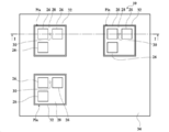
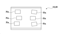
도 1 및 도 2는 각각 광전자 장치의 일 실시형태의, 부분적으로 간략화된 측단면도 및 상면도이다.
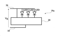
도 3은 도 1 및 도 2에 도시된 광전자 장치의 표시 픽셀의 등가 전기 다이어그램이다.
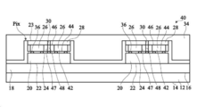
도 4a 및 도 4b는 광전자 장치의 다른 실시형태의 부분 개략 측면도이다.
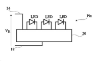
도 5는 도 4b에 도시된 광전자 장치의 표시 픽셀의 등가 전기 다이어그램이다.
도 6은 광전자 장치 제조 방법의 장점을 나타내는 도 1 및 도 2에 도시된 광전자 장치의 부분 개략 상면도이다.
도 7은 도 1 또는 도 4에 도시된 광전자 장치의 제어를 나타내는 다이어그램이다.
도 8a 및 도 8b는 광전자 장치의 다른 실시형태의 부분 개략 상면도이다.
도 9는 광전자 장치의 다른 실시형태의 부분 개략 측단면도이다.
도 10 내지 도 12는 광전자 장치의 다른 실시형태의 부분 개략 상면도이다.
도 13 및 도 14는 각각 제어될 표시 픽셀에 연결된 도전성 스트립(strip)에 인가되는 전위와 제어될 표시 픽셀의 전원 공급 단자들 사이에서 보여지는 전압의 타이밍 다이어그램이다.
도 15는 표시 픽셀의 일 실시형태의 등가 전기 다이어그램을 보여준다.
도 16은 도 15의 표시 픽셀의 일부분의 등가 전기 다이어그램을 보여준다.
도 17은 도 15의 표시 픽셀의 동작 중의 신호의 타이밍 다이어그램을 보여준다.
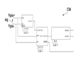
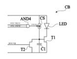
도 18 내지 도 21은 도 15의 표시 픽셀의 부분의 등가 전기 다이어그램을 보여준다.
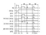
도 22는 도 18에 도시된 실시형태와 관련된 제어 유닛을 갖는 표시 픽셀의 동작 중의 신호의 타이밍 다이어그램을 보여준다.
도 23은 표시 픽셀의 다른 실시형태의 등가 전기 다이어그램을 보여준다.
도 24 및 도 25는 도 23의 표시 픽셀의 부분의 등가 전기 다이어그램을 보여준다.
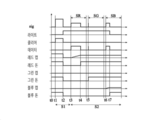
도 26은 도 23의 표시 픽셀의 동작 중의 신호의 타이밍 다이어그램을 보여준다.
도 27a 내지 도 27i는 도 1 및 도 2에 도시된 광전자 장치를 제조하는 방법의 또 다른 실시형태의 연속적인 스텝으로 얻은 구조의 부분 개략 측단면도이다.
도 28a 내지 도 28d는 도 4b에 도시된 광전자 장치를 제조하는 방법의 또 다른 실시 형태의 연속적인 스텝으로 얻은 구조의 부분 개략 측단면도이다.The above-described features and other features and advantages will be described in detail in the description of the specific embodiments below, which are not limited thereto in connection with the accompanying drawings.
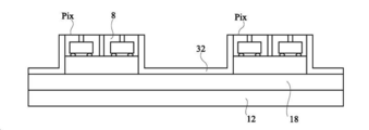
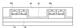
1 and 2 are partially simplified side and top views, respectively, of an embodiment of an optoelectronic device.
3 is an equivalent electrical diagram of display pixels of the optoelectronic device shown in FIGS. 1 and 2.
4A and 4B are partial schematic side views of another embodiment of an optoelectronic device.
5 is an equivalent electrical diagram of display pixels of the optoelectronic device shown in FIG. 4B.
6 is a partial schematic top view of the optoelectronic device shown in FIGS. 1 and 2 showing the advantages of the method of manufacturing the optoelectronic device.
FIG. 7 is a diagram showing control of the optoelectronic device shown in FIG. 1 or FIG. 4.
8A and 8B are partial schematic top views of another embodiment of an optoelectronic device.
9 is a partially schematic side cross-sectional view of another embodiment of an optoelectronic device.
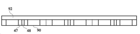
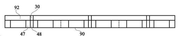
10 to 12 are partial schematic top views of another embodiment of an optoelectronic device.
13 and 14 are timing diagrams of voltages shown between a potential applied to a conductive strip connected to a display pixel to be controlled and power supply terminals of the display pixel to be controlled, respectively.
15 shows an equivalent electrical diagram of one embodiment of a display pixel.
FIG. 16 shows an equivalent electrical diagram of a portion of the display pixel of FIG. 15.
17 shows a timing diagram of a signal during operation of the display pixel of FIG. 15.
18 to 21 show equivalent electrical diagrams of portions of the display pixels of FIG. 15.
22 shows a timing diagram of a signal during operation of a display pixel having a control unit related to the embodiment shown in FIG. 18.
23 shows an equivalent electrical diagram of another embodiment of a display pixel.
24 and 25 show equivalent electrical diagrams of portions of the display pixels of FIG. 23.
FIG. 26 shows a timing diagram of a signal during operation of the display pixel of FIG. 23.
27A-27I are partial schematic side cross-sectional views of structures obtained in successive steps of another embodiment of the method of manufacturing the optoelectronic devices shown in FIGS. 1 and 2.
28A to 28D are partial schematic side cross-sectional views of structures obtained in successive steps of another embodiment of a method of manufacturing the optoelectronic device shown in FIG. 4B.
명확성을 위하여, 동일한 구성요소는 각각의 도면에서 동일한 참조번호로 지정되며, 또한 일반적으로, 전자 회로의 표시에 있어서, 각 도면은 일정한 비율로 되어 있지 않다. 또한, 본 명세서의 이해에 유용한 소자들만을 도시하고 설명할 것이다. 특히, 발광 다이오드의 구조는 당업자에게 잘 공지되어 있으므로 상세하게 설명하지 않는다.For the sake of clarity, the same components are designated by the same reference numerals in the respective drawings, and in general, in the display of the electronic circuit, each drawing is not in a constant ratio. In addition, only elements useful for understanding the present specification will be shown and described. In particular, the structure of the light emitting diode is well known to those skilled in the art and will not be described in detail.
이하의 설명에 있어서, 용어 "상부", "하부", "높은", "낮은" 등과 같은 상대적 위치를 한정하는 용어가 언급될 때에는, 도면의 방향이 언급되거나 또는 사용의 일반적인 위치에서의 광전자 장치가 언급된다. 별도의 설명이 없다면, 용어 "거의", "약" 및 "의 정도"의 표현은, 10% 내, 바람직하게는 5% 내를 의미한다. 또한, 발광 다이오드의 "활성 영역"은 발광 다이오드에 의하여 공급되는 전자기 방사선의 대부분이 방출되는 발광 다이오드의 영역을 나타낸다. 또한, 제1 상수 상태, 예를 들어, "0"이라고 된 낮은 상태와 제2 상수 상태, 예를 들어 "1"이라고 된 높은 상태 사이에서 교차하는 신호를 "이진수 신호" 라고 한다. 동일한 전자 회로의 상이한 이진수 신호의 높고 낮은 상태는 상이할 수 있다. 특히 이진수 신호는, 높은 또는 낮은 상태에서 완전하게 일정하지 않을 수 있는 전압이나 또는 전류에 대응한다.In the following description, when reference is made to terms that define relative positions, such as the terms "top", "bottom", "high", "low", etc., the orientation of the drawings is referred to, or the optoelectronic device at the general location of use Is mentioned. Unless otherwise specified, expressions of the terms "almost", "about" and "degree" mean within 10%, preferably within 5%. Further, the "active region" of the light emitting diode indicates the region of the light emitting diode in which most of the electromagnetic radiation supplied by the light emitting diode is emitted. In addition, a signal intersecting between a first constant state, for example, a low state called "0" and a second constant state, for example a high state called "1", is called a "binary signal". The high and low states of different binary signals of the same electronic circuit can be different. In particular, binary signals correspond to voltages or currents that may not be completely constant in high or low states.
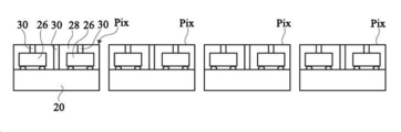
도 1 및 도 2는, 예를 들어 표시 화면 또는 화상 투사 장치에 대응하며, 표시 픽셀을 구비하는 광전자 장치(10)의 일 실시형태를 보여주며, 도 1에서는 2개의 표시 픽셀이 도시되어 있고, 도 2에서는 3개의 표시 픽셀이 도시되어 있다. 도 1은 II-II 선을 따르는 도 2의 단면도이며 도 2는 I-I 선을 따르는 도 1의 단면도이다.1 and 2, for example, correspond to a display screen or an image projection device, and show an embodiment of an
장치(10)는, 도 1의 하부에서 상부로,
바람직하게는 평행한, 대향하는 상부 표면 및 하부 표면(14, 16)을 구비하는 지지대(12)와,A
상부 표면(16)을 덮고 있는 전기적 도전층(18)을 구비하는 제1 전극층(18)과,A
전극층(18)에 놓여 전극층(18)과 접촉하고 있으며, 하부 표면(22)과 하부 표면에 대향하는 상부 표면(23)을 구비하는, 이후 표시 픽셀 회로라고도 불리는, 표시 픽셀(Pix)A display pixel (Pix), hereinafter also referred to as a display pixel circuit, which is placed on the
을 구비하며, 각 표시 픽셀(Pix)은And each display pixel Pix
전자 회로(20)로서, 이후 제어 회로라고 불리며, 하부 표면(22)과 하부 표면에 대향하는 상부 표면(24)을 구비하며, 그 표면들(22, 24)은 바람직하게는 평행하며, 하부 표면(22)은 전극층(18)에, 예를 들어 접착 재료를 통하여 접착되어 있는 전자회로(20)와,As the
전자 회로(20)의 상부 표면(24)에 접착된 광전자 회로(26)로서, 도 2에서는 표시 픽셀(Pix)당 3개의 광전자 회로(26)가 도시되어 있으며, 각 광전자 회로(26)는 하나 이상의 발광 다이오드(도시되지 않음)를 구비하고 있는 광전자 회로(26)와,As an
광전자 회로(26)를 덮고 있으며, 광전자 회로(26) 사이의 제어 회로(20)의 상부 표면(24)을 덮고 있는 전기적-절연부(28)와,An electrical-insulating
절연부(28)를 가로지르고 있으며, 광전자 회로(26) 및 제어 회로(20)의 상부 표면(24)과 접촉하고 있는 전기적-도전성 소자(30)와, An electro-
표시 픽셀(Pix) 사이의 전극층(18)을 덮고 있으며, 전자 회로(20)의 측면 및 가능한 한 절연부(28)의 측면을 커버하는 전기적-절연층(32)과,An electrical-insulating
발광 다이오드에 의하여 방출된 방사선을 적어도 부분적으로 투과시키는 전기적 도전층을 구비하는 제2 전극층(34)으로서, 도전층(34)은 절연층(32)과 절연부(28)을 덮고 있으며 각 표시 픽셀(Pix)의 도전성 소자(30)와 접촉하고 있는 제2 전극층(34)을 구비하고 있다.As a
도시되지 않은, 캡슐화층이 도전층(34)을 덮을 수 있다.An encapsulation layer, not shown, may cover the
전자 회로(20)의 하부 표면(22)이 접착 재료에 의하여 전극층(18)에 접착될 때, 접착 재료는 바람직하게는 전기적 도전성이다. 변형으로서, 예를 들어, 전자 회로(20)의 하부 표면(22)의 주변에 배열된, 전기적 도전성이 아닌 접착 재료가 사용될 수 있다.When the
일 실시형태에 따르면, 각 광전자 회로(26)는 하나 이상의 발광 다이오드를 구비한다. 광전자 회로(26)가 2 이상의 발광 다이오드를 구비하는 경우에는, 광전자 회로(26)의 모든 발광 다이오드는 바람직하게는 실질적으로 동일한 파장의 광 방사선을 방출한다.According to one embodiment, each
각 발광 다이오드는 활성 영역을 포함하는 실질적으로 평면인 반도체층의 적층을 구비하는 소위 2차원 발광 다이오드에 대응할 수 있다. 각 발광 다이오드는, 3차원 반도체 소자, 특히 마이크로와이어, 나노와이어, 원뿔, 절두체, 각뿔, 또는 각뿔대를 덮고 있는 반도체 쉘을 구비하는 방사 구조를 갖는 하나 이상의 3차원 발광 다이오드를 구비할 수 있으며, 그 쉘은 활성 영역을 포함하는 비-평면 반도체층의 적층으로 형성된다. 그런 발광 다이오드의 예는 특허 출원 US2014/0077151호 및 US2016/0218240호에 개시되어 있다. 각 발광 다이오드는, 쉘이 반도체 소자의 축 방향 연장으로 배치된 축방향 구조를 갖는 하나 이상의 3차원 발광 다이오드를 구비할 수 있다.Each light emitting diode can correspond to a so-called two-dimensional light emitting diode having a stack of substantially planar semiconductor layers comprising an active region. Each light emitting diode may include one or more three dimensional light emitting diodes having a radiating structure having a semiconductor shell covering a three dimensional semiconductor device, particularly a microwire, nanowire, cone, frustum, pyramid, or pyramid, the The shell is formed of a stack of non-planar semiconductor layers comprising active regions. Examples of such light emitting diodes are disclosed in patent applications US2014 / 0077151 and US2016 / 0218240. Each light emitting diode may include one or more three-dimensional light emitting diodes having an axial structure in which the shell is disposed in an axial extension of the semiconductor element.
각 표시 픽셀(Pix)에 대하여, 광전자 회로(26)는 "플립-칩"형 접속에 의하여 제어 회로(20)에 접착될 수 있다. 광전자 회로(26)를 제어 회로(20)에 결합시키는 가용성의 도전성 소자(36), 예를 들어, 솔더볼 또는 인듐볼은 광전자 회로(26)와 제어 회로(20) 사이의 기계적 결합을 강화하고, 또한, 발광 다이오드 또는 광전자 회로(26)의 발광 다이오드를 전자 회로(20)에 전기 접속하는 것을 강화한다. 또 다른 실시형태에 따르면, 각 광전자 회로(26)는 직접 접착에 의하여 제어 회로(20)에 접착될 수 있다.For each display pixel Pix, the
일 실시형태에 따르면, 각 표시 픽셀(Pix)은 적어도 2 형태의 광전자 회로(26)를 구비한다. 제1 형태의 광전자 회로(26)는 제1 파장의 제1 방사선을 방출할 수 있으며, 제2 형태의 광전자 회로(26)는 제2 파장의 제2 방사선을 방출할 수 있다. 일 실시형태에 따르면, 각 표시 픽셀(Pix)은 적어도 3 형태의 광전자 회로(26)를 구비하며, 제3 형태의 광전자 회로는 제3 파장의 제3 방사선을 방출할 수 있다. 제1, 제2 및 제3 파장은 상이할 수 있다.According to one embodiment, each display pixel Pix has at least two types of
일 실시형태에 따르면, 제1 파장은 청색광에 대응하며 430nm 내지 490nm 의 범위 내에 있다. 일 실시형태에 따르면, 제2 파장은 녹색광에 대응하며 510nm 내지 570nm의 범위 내에 있다. 일 실시형태에 따르면, 제3 파장은 적색광에 대응하며 600nm 내지 720nm의 범위 내에 있다.According to one embodiment, the first wavelength corresponds to blue light and is in the range of 430 nm to 490 nm. According to one embodiment, the second wavelength corresponds to green light and is in the range of 510 nm to 570 nm. According to one embodiment, the third wavelength corresponds to red light and is in the range of 600 nm to 720 nm.
일 실시형태에 따르면, 각 표시 픽셀(Pix)은 제4 형태의 광전자 회로(26)를 구비하며, 제4 형태의 광전자 회로(26)는 제4 파장의 제4 방사선을 방출할 수 있다. 제1, 제2, 제3 및 제4 파장은 상이할 수 있다. 일 실시형태에 따르면, 제4 파장은 노랑색광에 대응하며 570nm 내지 600nm의 범위에 있다. 또 다른 실시형태에 따르면, 제4 방사선은 적외선에 근접한 방사선, 특히 700nm와 980nm 사이의 방사선, 자외선 방사선, 또는 백색광에 대응한다.According to one embodiment, each display pixel Pix has a fourth type of
각 광전자 회로(26)는 그 위에 놓여 있는 발광 다이오드 또는 발광 다이오드를 갖는 반도체 기판을 구비할 수 있다. 예를 들어, 반도체 기판은 실리콘, 게르마늄, 실리콘 카바이드, GaN 또는 GaAs 등의 III-V 화합물 등으로 이루어진 기판, ZnO 기판, 또는 사파이어 기판이다. 또 다른 실시형태에 따르면, 각 광전자 회로(26)는 기판을 구비하지 않는 것도 가능하다. 이때 발광 다이오드 또는 발광 다이오드들과 접촉하고 있는 광전자 회로(26)의 하부 표면에 미러(mirror)층이 배치될 수 있다. 일 실시형태에 따르면, 미러층은 발광 다이오드에 의하여 방출된 방사선을 적어도 부분적으로 반사할 수 있다.Each
각 제어 회로(20)는 발광 다이오드를 제어하기 위하여 사용되는, 도시되지 않은 전자 구성요소, 특히 트랜지스터를 구비할 수 있다. 각 제어 회로(26)는 그의 내부 및/또는 상부에 형성된 전자 구성품을 갖는 반도체 기판을 구비할 수 있다. 이 때, 제어 회로(20)의 하부 표면(22)은 전자 구성품이 형성된 측인 기판의 앞 표면에 대향하는 기판의 뒷 표면에 대응할 수 있다. 반도체 기판은, 예를 들어, 실리콘, 특히 단결정 실리콘으로 만들어진 기판이다.Each
바람직하게는 광전자 회로(26)는 발광 다이오드와 발광 다이오드의 접속 소자만을 구비하며, 제어 회로(20)는 광전자 회로(26)의 발광 다이오드를 제어하기에 필요한 모든 전자 구성품을 구비한다. 변형으로서, 광전자 회로(26)는 발광 다이오드에 부과하여 다른 전자 구성품도 구비할 수 있다.Preferably, the
광전자 장치(10)는 10 내지 109 개의 표시 픽셀(Pix)을 구비할 수 있다. 각 표시 픽셀(Pix)은 상면도에서 1㎛2 내지 100㎜2 범위의 표면 영역을 차지할 수 있다. 각 표시 픽셀(Pix)의 두께는 100㎛ 내지 10㎜ 범위에 있을 수 있다. 각 전자 회로(20)의 두께는 1㎛ 내지 2,000㎛ 범위에 있을 수 있다. 각 광전자 회로(26)의 두께는 0.2㎛ 내지 1,000㎛ 범위에 있을 수 있다.The
지지대(12)는, 예를 들어, 폴리머, 특히 에폭시 수지, 특히 인쇄 회로 제조를 위해 사용되는 FR4 재료와, 또는, 금속 재료, 예를 들어 알루미늄을 구비하는 전기적-절연 재료로 이루어진다. 지지대(12)의 두께는 100㎛ 내지 10㎜ 범위에 있다.The
도전층(18)은 바람직하게는 금속층, 예를 들어, 알루미늄, 은, 구리 또는 아연에 대응한다. 도전층(18)의 두께는 0.5㎛ 내지 1,000㎛ 범위에 있을 수 있다.The
각 절연부(28)는 유전체 재료, 예를 들어, 실리콘산화물(SiO2), 실리콘질화물(SixNy, 여기서 x는 약 3과 같으며 y는 약 4와 같고, 예를 들면, Si3N4), 실리콘산질화물(SiOxNv, 여기서 x는 약 1/2과 같고, y는 약 1과 같으며, 예를 들면 Si2ON2), 알루미늄산화물(Al2O3) 또는 하프늄산화물(HfO2)로 이루어질 수 있다. 각 절연부(28)의 최대 두께는 0.5㎛ 내지 1,000㎛ 범위에 있을 수 있다.Each insulating
각 도전성 소자(30)는 구리, 티타늄, 니켈, 금, 주석, 알루미늄 및 2 이상의 이들 화합물의 합금을 구비하는 그룹으로부터 선택된 재료로 만들어질 수 있다.Each
절연층(32)은, 유전체 재료, 예를 들어, 실리콘산화물(SiO2), 실리콘질화물(SixNy, 여기서 x는 약 3과 같으며 y는 약 4와 같고, 예를 들면, Si3N4), 실리콘산질화물(SiOxNv, 여기서 x는 약 1/2과 같고, y는 약 1과 같으며, 예를 들면 Si2ON2), 알루미늄산화물(Al2O3) 또는 하프늄산화물(HfO2)로 이루어질 수 있다. 절연층(32)의 두께는 0.02㎛ 내지 1,000㎛ 범위에 있을 수 있다. 바람직하게는, 절연층(32)은 불투명하다. 절연층(32)은 백색 수지, 흑색 수지, 또는, 특히 티타늄산화물 입자로 채워진 투명 수지에 대응할 수 있다.The insulating
도전층(34)은 발광 다이오드에 의하여 방출된 전자기 방사선을 통과시킬 수 있다. 도전층(34)을 형성하는 재료는, 인듐주석산화물(ITO), 알루미늄 또는 갈륨 아연 산화물, 또는 그래핀 등의 투명 도전성 재료일 수 있다. 표시 픽셀(Pix) 상의 전기적-도전층(34)의 최소 두께는 0.1㎛ 내지 1,000㎛ 범위에 있을 수 있다.The
캡슐화층은 적어도 부분적으로 투명 절연 재료로 만들어질 수 있다. 캡슐화층은 적어도 부분적으로 투명 무기 재료로 만들어질 수 있다. 예로서, 무기 재료는, SiOx 형태(여기서 x는 1 및 2 사이의 실수), 또는 SiOyNz 형태(여기서 y 및 z는 0과 1 사이의 실수)의 실리콘 산화물, 알루미늄 산화물, 예를 들어 Al2O3를 구비하는 그룹으로부터 선택된다. 캡슐화층은 적어도 부분적으로 투명 유기 재료로 이루어진다. 예로서, 캡슐화층은 실리콘폴리머, 에폭시폴리머 및 아크릴릭폴리머 또는 폴리카보네이트이다.The encapsulation layer can be at least partially made of a transparent insulating material. The encapsulation layer can be at least partially made of a transparent inorganic material. By way of example, the inorganic material is a silicon oxide, aluminum oxide, for example in the form of SiOx (where x is a real number between 1 and 2), or SiO y N z form (where y and z are real numbers between 0 and 1), for example Al 2 O 3 is selected from the group. The encapsulation layer is at least partially made of a transparent organic material. As an example, the encapsulation layer is a silicone polymer, an epoxy polymer and an acrylic polymer or polycarbonate.
일 실시형태에 따르면, 작동에 있어서, 전압(VE)이 표시 픽셀(Pix)의 공급을 위하여, 특히 표시 픽셀(Pix)의 광전자 회로(26)의 발광 다이오드의 공급을 위하여전극층(34 및 18) 사이에 인가된다.According to one embodiment, in operation, the voltage V E is applied to the electrode layers 34 and 18 for the supply of the display pixel Pix, especially for the supply of the light emitting diodes of the
도 3은 도 1 및 도 2에 도시된 표시 픽셀(Pix)의 등가 전기 다이어그램을 보여준다. 각 발광 다이오드(LED)의 제1 전극, 예를 들어 캐소드가 표시 픽셀(Pix)의 제어 회로(20)에 접속되어 있고, 동시에, 각 발광 다이오드(LED)의 제2 전극, 예를 들어 애노드가 전극층(34)에 접속되어 있다. 제어 회로(20)는 전극층(18 및 34) 사이에 접속되어 있으며, 전압(VE)을 수신한다. 회로(20)는 광전자 회로(26)의 발광 다이오드를 제어한다.3 shows an equivalent electrical diagram of the display pixel Pix illustrated in FIGS. 1 and 2. The first electrode of each light emitting diode (LED), for example the cathode, is connected to the
도 4a 는, 광전자 장치(10)의 모든 소자를 구비하는, 도 1과 유사한 다른 실시형태의 광전자 장치(37)의 도면으로서, 절연층(32)이 존재하지 않고 전극층(34)이 기판(38)에 놓여 있다는 차이점을 갖는다. 광전자 장치(37)를 제조하는 방법은, 지지대(12)에 전극층(18)을 형성하고, 전극층(18)에 표시 픽셀(Pix)를 조립하고, 기판(38)에 전극층(34)을 형성하고, 전극층(34)에 표시 픽셀(Pix)을 붙인다. 지지대(12)와 기판(38)은 플렉시블하며, 이것은 플렉시블한 광전자 장치(37)를 제조할 수 있게 한다.FIG. 4A is a view of an
도 4b는, 광전자 장치(10)의 모든 소자를 구비하는, 도 1과 유사한 다른 실시형태의 광전자 장치(40)의 도면으로서, 각 표시 픽셀(Pix)에 대하여, 광전자 회로들(26)은 표시 픽셀(Pix)의 제어 회로(20)의 상부 표면(24)을 커버하는 단일 광전자 회로(42)에 통합되어 있으며 제어 회로(20)의 상부 표면(24)에, 예를 들어 가용성 도전성 소자(36)에 의하여 접착된다. 각 광전자 회로(42)는 바람직하게는 평행한, 대향하는 하부 표면 및 상부 표면(44, 46)을 구비하며, 광전자 회로(42)의 하부 표면(44)은 제어 회로(20)의 상부 표면(24)에 접착된다. 광전자 회로(42)는, 예를 들어, 광전자 회로(42)의 부분(47) 내에 형성된 하나 이상의 관통 수직 접속(48) 또는 TSV(관통 실리콘 비아)를 구비하며, 이것은 상부 표면(46)과 하부 표면(44)을 연결하며 광전자 회로(42)의 나머지와는 전기적으로 절연되어 있다. 부분(47)은 전기적-절연 재료 또는 반도체 재료로 만들어질 수 있다. 후자의 경우에, TSV(48)는 전기적-절연층으로 둘러싸여진다. 각 광전자 회로(42)의 상부 표면(46)은 절연부(28)로 덮여 있다. 절연부(28)는 TSV(48)와 접촉하는 전기적-도전 소재(30)에 의하여 가로질러져 있다. 또 다른 실시형태에 따르면, 제어 회로(20)의 전원 공급은 TSV(48) 이외의 다른 수단으로 얻어진다.FIG. 4B is a view of an
일 실시형태에 따르면, 각 TSV(48)는 전기적-절연층으로 둘러싸인, 전기적-도전 재료, 예를 들어, 폴리실리콘, 텅스텐, 구리, 알루미늄 또는 내화 금속 재료로 이루어진 코어를 구비할 수 있다.According to one embodiment, each
각 광전자 회로(42)는 제1 파장의 제1 방사선을 방출할 수 있는 하나 이상의 제1 발광 다이오드와 제2 파장의 제2 방사선을 방출할 수 있는 제2 발광 다이오드를 구비한다. 각 광전자 회로(42)는 제3 파장의 제3 방사선을 방출할 수 있는 하나 이상의 제3 발광 다이오드를 더 구비할 수 있다.Each
도 5는, 각 광전자 회로(42)가 3개의 발광 다이오드를 구비하는 경우에 도 3에 도시된 표시 픽셀(Pix)의 등가 전기 다이어그램을 보여준다. 이 실시형태에 있어서, 광전자 회로(42)의 각 발광 다이오드의 두 전극은 표시 픽셀(Pix)의 제어 회로(20)에 접속되어 있다. 제어 회로(20)는 전극층(18 및 34) 사이에 접속되어 있으며 전압(VE)을 수신한다. 회로(20)는 광전자 회로(26)의 발광 다이오드(LED)를 제어한다.FIG. 5 shows an equivalent electrical diagram of the display pixel Pix shown in FIG. 3 when each
본 실시형태에 있어서, 도전층(18)은 광전자 회로(10,40)의 모든 표시 픽셀(Pix)과 접촉하고 있으며 도전층(34)은 광전자 장치(10, 40)의 모든 표시 픽셀(Pix)과 접촉하고 있다.In this embodiment, the
광전자 장치(10 또는 40)를 제조하는 방법의 일 실시형태는 표시 픽셀(Pix)을 제조하고 전극층(18)에 각 표시 픽셀(Pix)를 분리되게 설치하는 것을 구비한다. 일 실시형태에 따르면, 전극층(18 및 34)은 모든 표시 픽셀(Pix)에 공통이며, 표시 픽셀(Pix)의 접속은 간단하게 되어 있고, 전극층(18) 상에 각 표시 픽셀(Pix)의 배치가 높은 정확도를 가지고 실행될 필요가 없다. 이것은 전극층(18) 상에 표시 픽셀(Pix)을 배열하기 위한 비용을 감소시키면서 더 빠른 기술을 실행할 수 있게 한다. 또한, 발광 다이오드는 표시 픽셀(Pix)의 전자 회로(20) 상에 이미 조립되어 있기 때문에, 광전자 장치(10 또는 40)의 조립 중에 실행될 이송의 수를 감소시킨다. 본 실시형태에 있어서, 각 표시 픽셀(Pix)은 거기에 저장된 픽셀의 식별자를 갖는 메모리를 구비할 수 있다. 제조 방법은, 그 식별자에 따라서 각 표시 픽셀(Pix)의 위치를 되찾는 보정 단계를 구비할 수 있다. 그리고, 동작에 있어서는, 데이터가 그들 식별자에 따라서 픽셀로 전송될 수 있다.One embodiment of a method for manufacturing the
도 6은, 표시 픽셀(Pix)이 아주 정확하게 배열되지 않을 수 있고, 예를 들어, 열(row)과 행(column)에서 완벽하게 정렬되어 있을 수 있고 어떤 표시 픽셀(Pix)은 열 및 행의 방향에 대하여 경사질 수 있는 사실을 나타내는 광전자 장치(10 또는 40)의 개략 상면도를 보여준다.6, the display pixels Pix may not be arranged very accurately, for example, may be perfectly aligned in rows and columns, and some display pixels Pix may be arranged in columns and rows. It shows a schematic top view of an
전술된 실시형태에 있어서, 전극층(18)은 모든 표시 픽셀(Pix)에 접속되어 있으며 지지대(12)의 대부분 또는 심지어 전체 상에서 연장하는 연속된 층의 형태로 나타나 있다. In the above-described embodiment, the
각 표시 픽셀(Pix)에 대하여, 제어 회로(20)는 제어 신호를 수신할 수 있으며, 수신된 제어 신호로부터 표시 픽셀의 발광 다이오드를 제어할 수 있으며, 특히 표시 픽셀에 의하여 방출된 광의 음영, 채도 및 밝기를 제어할 수 있다.For each display pixel Pix, the
일 실시형태에 따르며, 제어 신호는 전압(VE)의 변조에 의하여 표시 픽셀(Pix)의 제어 회로(20)로 전송된다.According to one embodiment, the control signal is transmitted to the
도 7은 제어 신호(COM)를 수신하고, 제어 신호(COM)로 변조되어 있는, 표시 픽셀(Pix)로의 전원공급을 위한 전압(VE)을 광전자 장치(10 및 40)로 공급할 수 있는 처리 유닛(49)을 매우 개략적으로 보여준다. 처리 유닛(49)은 전용 회로에 대응될 수 있거나, 또는 메모리 내에 기억된 컴퓨터 프로그램의 지시를 실행할 수 있는 프로세서, 예를 들어, 마이크로프로세서 또는 마이크로제어기를 구비할 수 있다.7 is a process for receiving the control signal COM and supplying the voltage V E for supplying power to the display pixel Pix modulated by the control signal COM to the
각 표시 픽셀(Pix)의 제어 회로(20)는 전압(VE)의 복조에 의하여 제어 신호(COM)를 추출할 수 있다. 이때, 제어 회로(20)는, 제어 신호(COM)가 거기로 어드레스 되었는지 여부를 판단할 수 있다. 예로서, 식별자가 각 표시 픽셀(Pix)과 관련될 수 있고, 전압(VE)의 복조에 의하여 얻어진 제어 회로(COM)는, 제어 신호가 의도하는 표시 픽셀의 식별자를 구비할 수 있다.The
유익하게는, 표시 픽셀(Pix)의 활성 어드레싱이 실행될 수 있다. 사실, 각 제어 회로(20)는, 새로운 제어 신호를 수신할 때까지, 표시 픽셀의 표시 특성, 특히 음영, 채도 및 밝기의 유지를 제어할 수 있다.Advantageously, active addressing of the display pixel Pix can be performed. In fact, each
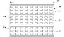
도 8a는 광전자 장치(10 또는 40)의 모든 소자를 구비하고 있는 다른 실시형태의 광전자 장치(50)의 개략 상면도로서, 전극층(18)이 지지대(12) 상에서 연장하는, 평행한 전기적-도전성 스트립(52)으로 분리되어 있으며, 도 8에는 3개의 스트립(52)이 예로서 도시되어 있다. 표시 픽셀(Pix)의 하나 이상의 열이 각 도전성 스트립에 분포되어 있다. 바람직하게는, 표시 픽셀(Pix)의 복수의 열이 각 도전성 스트립(52)에 분포되어 있는데, 예로서, 도 8에는, 도전성 스트립(52) 당 3개의 열의 표시 픽셀(Pix)이 도시되어 있다.FIG. 8A is a schematic top view of an
또 다른 실시형태에 따르면, 전극층(18) 및/또는 전극층(34)은 분리된 전극부로 나누어질 수 있다. 또 다른 실시형태에 따르면, 전극층(34)은 또한 평행한 전기적-도전성 스트립으로 나누어질 수 있다. 전극층(18 및 34)이 각각 스트립으로 나누어질 때, 전극층(18)의 스트립들은 바람직하게는 전극층(34)의 스트립과 실질적으로 동일한 크기를 가지며, 전극층(34)의 각 스트립은 바람직하게는 전극층(18)의 스트립 중 하나를 실질적으로 덮는다. 또 다른 실시형태에 따르면, 전극(18 또는 34) 중 하나는 표시 픽셀(Pix)에 공통일 수 있으며 동시에 다른 전극(18 또는 34)은 평행한 전기적-도전성 스트립으로 분리된다. 전극층(18, 34)이 표시 픽셀의 조립체를 사이에 끼우는 적층된 스트립으로 분리되는 이 실시형태에 있어서, 상이한 제어 신호가 각 표시 픽셀 조립체에 대하여 상이하게 전압(VE)을 변조함으로써 병렬로 전송된다. 이것은 각 표시 픽셀의 조립체에 대하여 제어 신호를 병렬로 전송할 수 있게 한다. 이것은 전자기 방사선의 변조 주파수를 감소시키거나 및/또는 전송되는 데이터의 속도를 증가시킬 수 있게 한다.According to another embodiment, the
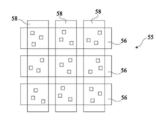
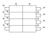
도 8b는 광전자 장치(55)의 다른 실시형태의 부분 개략 상면도로서, 여기서 전극층(18)은 열 방향을 따라서 연장하는 도전성 스트립(56)으로 분리되어 있으며 전극층(34)은 행 방향을 따라서 연장하고 있으며, 행 전극으로 불리는 도전성 스트립(58)으로 분리되어 있다. 하나 이상의 표시 픽셀(Pix)이 각 열 전극(56)과 각 행 전극(58) 사이의, 상면도에서의 교차지점에 배열되어 있으며, 열 전극(56)과 행 전극(58)에 접속되어 있다. 예로서, 도 8b에서는, 3개의 표시 픽셀(Pix)이, 각 열 전극(56)과 각 행 전극(58)의, 상면도에서의 교차지점에 제공되어 있으며 표시될 화상의 한 픽셀을 형성한다. 복수의 표시 픽셀(Pix)이 표시될 화상의 각각의 픽셀에 대하여 제공되는 경우, 이것은 표시 픽셀(Pix) 중 하나가 결함이 있는 경우에 리던던시(redundancy)를 가질 수 있게 한다.8B is a partial schematic top view of another embodiment of the
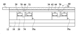
도 9는 광전자 장치(10)의 모든 소자를 구비하고 있는, 도 1과 유사한 또 다른 실시형태의 광전자 장치(60)의 도면이며, 전극층(34)을 덮고 있는 제1층(62)과 제2층(64)의 적층을 더 구비하고 있다. 층(62)은 층(64)을 형성하는 재료의 굴절율보다 큰 굴절율을 갖는 재료로 만들어진다. 층(62 및 64)은 표시 픽셀(Pix)에 의하여 방출된 방사선을 적어도 부분적으로 투과시킨다. 층(64)은, 예를 들어 유리, SiO2, Al2O3, HfO2, 유기 재료, 예를 들어, 폴리머, 특히 폴리(메틸 메타크릴레이트)(PMMA)로 이루어진다. 예를 들어, 층(62)은 공기막에 대응한다. 층(64)은, 예를 들어, 가시광 영역 내 또는 가시광 영역 밖, 특히 적외선과 자외선 영역 사이의 파장 영역의 전자기 방사선(66)의 도파관을 형성한다. 광전자 장치(60)는 층(64) 내에 그런 방사선(66)을 방출할 수 있는 광전자 회로(68)를 구비한다. 광전자 회로(68)는 층(64) 주변에 배치될 수 있으며, 그 측면 끝으로부터 층(64) 내에 방사선(66)을 방출할 수 있다. 적외 방사선은 전술된 제어 신호를 전송하기 위하여 변조된다. 일 실시형태에 따르면, 광학적 결합 수단(70)은 각 표시 픽셀(Pix)과 도파관(64) 사이에 제공되어서 도파관(64)에서 안내된 방사선(66)의 부분(72)이, 결합 수단(70)을 경유하여 각 표시 픽셀(Pix)의 레벨에서 빠져나온다. 예로서, 결합 수단(70)은, 각 표시 픽셀(Pix)과 층(64) 사이의 광학적 결합을 강화하기 위하여 각 표시 픽셀(Pix)의 반대측의 층(62) 및/또는 층(64) 상에 제공된 텍스처링(trxturing)에 대응한다. 예를 들어 결합 수단(70)은, 도파관(64)에서 전파하는 전자기 방사선의 부분을 관련 표시 픽셀(Pix)을 향하여 반사하게 할 수 있는 회절 격자에 대응한다.FIG. 9 is a view of an
각 표시 픽셀(Pix)은, 예를 들어 포토다이오드 또는 포토레지스터의 광전자 회로(68)에 의하여 방출되는 방사선을 검출할 수 있는 하나 이상의 센서(74)를 구비하며, 그 센서는, 예를 들어 표시 픽셀(Pix)에 의하여 수신된 방사선(72)의 강도를 나타내는 전기 신호를 제어 회로(20)에 제공한다. 제어 회로(20)는 센서에 접속되어 있으며, 센서에 의하여 공급된 측정 신호에 기초하여 제어 신호를 추출할 수 있다.Each display pixel Pix includes, for example, one or
일 실시형태에 따르면, 제어 신호를 이송하는 동일한 전자기 방사선이 모든 표시 픽셀로 전송된다. 또 다른 실시형태에 따르면, 복수의 도파관이 제공될 수 있으며, 각 도파관은 표시 픽셀의 조립체와 연관되어 있다. 또 다른 실시형태에 따르면, 광학적 연속성 중단 영역을 도파관 내에 형성할 수 있어서, 다른 그룹의 픽셀을 어드레스 할 수 있도록 한다.According to one embodiment, the same electromagnetic radiation carrying a control signal is transmitted to all display pixels. According to another embodiment, a plurality of waveguides may be provided, each waveguide being associated with an assembly of display pixels. According to another embodiment, an optical continuity interruption region can be formed in the waveguide, allowing different groups of pixels to be addressed.
도 10은 분리된 도파관(82) 또는 광학적 불연속성을 갖는 단일 도파관을 구비하는 다른 실시형태의 광전자 장치(80)의 부분 개략 상면도로서, 각각은 도시하지 않은 표시 픽셀의 조합체를 덮고 있다. 광전자 장치(80)는, 각각이 비가시광 영역의 전자기 방사선을 연관된 도파관(82)에서 방출할 수 있는 광전자 회로(84)를 더 구비하고 있다. 이것은 표시 픽셀(Pix)의 각 조합체에 대하여 제어 신호를 병렬로 전송할 수 있게 한다. 이것은 전자기 방사선의 변조 주파수를 감소 및/또는 전송된 데이터의 속도를 증가하게 할 수 있다.10 is a partial schematic top view of an optoelectronic device 80 of another embodiment having a
도 11은 광전자 장치(80)의 모든 소자를 구비하는 또 다른 실시형태의 광전자 장치(90)의 부분 개략 상면도로서, 각 분리된 도파관(82)은 하나 이상의 표시 픽셀 열을 덮고 있다.11 is a partial schematic top view of an
본 실시형태에 있어서, 전극층(34) 또는 전극층(18)은 행 방향을 따라서 연장하는 도전성 스트립(92)으로 분리된다. 각 도전성 스트립(92)은 하나 이상의 픽셀 행의 표시 픽셀에 연결되어 있다.In the present embodiment, the
표시 픽셀 제어 방법의 실시형태는, 전극(18, 92)을 경유하여 표시 픽셀 또는 표시 픽셀 그룹의 선택 단계와, 그런 후 도파관(82) 중 하나에 의하여, 선택된 표시 픽셀의 일부로의 데이터 전송 단계를 구비한다. 그 선택 단계는 선택된 표시 픽셀에 연결된 도전성 스트립(92)을 제1 전위로 취하고 동시에 다른 도전성 스트립(92)은 제1 전위와는 상이한 제2 전위로 유지함으로써 실행될 수 있다. 선택된 표시 픽셀만이 활성화되며 전자기 방사선에 의하여 전송된 데이터를 처리할 수 있다. 다른 표시 픽셀은 비활성화되며 방사선에 의하여 전송된 데이터는 무시된다. 이때, 데이터를 이송하는 방사선은 관심 있는 픽셀을 커버하는 도파관(82)으로 방출된다. 선택되어 있고 도파관(82)으로 덮여있는 표시 픽셀만이, 도파관(82)에 의하여 전송된 방사선의 검출에 의하여 얻어진 데이터를 처리할 것이다.Embodiments of the display pixel control method include selecting a display pixel or a group of display pixels via
일 실시형태에 따르면, 각 도전성 스트립(92)은 표시 픽셀의 단일 행의 표시 픽셀에 연결되고 각 도파관(82)은 한 열의 표시 픽셀만을 덮는다. 이때 전술된 제어 방법은 단일 표시 픽셀만을 선택하고 데이터를 전송할 수 있게 한다.According to one embodiment, each
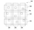
도 12는, 전극층(18)이 열 방향을 따라서 연장하는 도전성 스트립(102)으로 분리되어 열 전극이라고 불리는, 다른 실시형태의 광전자 장치(100)의 부분 개략 상면도로서, 각 도전성 스트립(102)은 한 픽셀 열의 표시 픽셀(Pix)에 연결되어 있으며, 전극층(34)는 행 방향을 따라서 연장하는 도전성 스트립(104)으로 분리되어 행 전극이라 불리며, 각 도전성 스트립(104)은 한 픽셀 행의 표시 픽셀(Pix)에 연결되어 있다.12 is a partially schematic top view of an
도 12에 도시된 바와 같이, 각 도전성 스트립(102)의 폭은 행 방향을 따라서 측정된 표시 픽셀(Pix)의 크기보다 크며 각 도전성 스트립(104)의 폭은 열 방향을 따라서 측정된 표시 픽셀(Pix)의 크기보다 크다. 따라서, 각 열에 대하여, 열에 속하는 표시 픽셀(Pix)은 완벽하게 정렬되지 않을 수 있다. 유사하게, 각 행에 대하여, 행에 속하는 표시 픽셀(Pix)은 완전하게 정렬되지 않을 수 있다.12, the width of each
표시 픽셀(Pix)을 제어하는 방법의 일 실시형태는 표시 픽셀의 선택 단계와 이어서 그 표시 픽셀(Pix)로의 데이터 전송 단계를 구비한다.One embodiment of a method for controlling a display pixel Pix comprises a step of selecting a display pixel followed by a step of transferring data to the display pixel Pix.
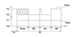
도 13은 제어될 표시 픽셀에 연결된 행 및 열 전극에 각각 인가된 전위 Vpix+ 및 Vpix- 각각의 타이밍 다이어그램이며 도 14는 제어될 표시 픽셀의 전원 공급 단자 사이에서 보여진 전압 sig의 타이밍 다이어그램이다.13 is a timing diagram of each of the potentials Vpix + and Vpix- respectively applied to the row and column electrodes connected to the display pixels to be controlled, and FIG. 14 is a timing diagram of the voltage sig shown between the power supply terminals of the display pixels to be controlled.
일 실시형태에 따르면, 광전자 회로(100)는 두 값 V0 및 V1(V1은 V0보다 큼) 사이에서 각 열 전극의 전위를 변화할 수 있고, 두 값 V2 및 V3(V3는 V2보다 크며 V2는 V1보다 큼) 사이에서 각 행 전극의 전위를 변화할 수 있다. V3 및 V2 사이의 차는 V1 및 V0 사이의 차와 같을 수 있다.According to one embodiment, the
일 실시형태에 따르면, 제어 방법은 제어될 표시 픽셀의 선택 단계 (S1)와, 이어서, 선택된 표시 픽셀로의 데이터 전송 단계(S2)를 구비한다.According to one embodiment, the control method includes a selection step (S1) of display pixels to be controlled, and then a data transmission step (S2) to the selected display pixels.
단계 S1은 제어될 표시 픽셀에 연결된 열 전극을 V0로 취하고, 다른 열 전극들은 V1으로 그대로 두며, 제어될 표시 픽셀에 연결된 행 전극을 V3로 취하고 다른 열 전극은 V2로 그대로 두는 것을 구비한다. 제어될 표시 픽셀은 V3-V0와 같은 전압을 보여주며, 동시에 동일한 열의 다른 표시 픽셀은 V2-V0와 같은 전압을 보여주며, 동일한 행의 다른 표시 픽셀은 V3-V1과 같은 전압을 보여주며 다른 열 및 행의 다른 표시 픽셀은 V2-V1과 같은 전압을 보여준다. 제어될 표시 픽셀 이외의 모든 다른 표시 픽셀은 V3-V0보다 작은 전압을 보여준다.Step S1 includes taking the column electrode connected to the display pixel to be controlled as V0, leaving the other column electrodes as V1, taking the row electrode connected to the display pixel to be controlled as V3, and leaving the other column electrode as V2. The display pixel to be controlled shows the same voltage as V3-V0, at the same time the other display pixels in the same column show the same voltage as V2-V0, and the other display pixels in the same row show the same voltage as V3-V1 and different columns And other display pixels in the row show the same voltage as V2-V1. All display pixels other than the display pixel to be controlled show a voltage less than V3-V0.
단계 S2는 V2와 V3 사이에서 제어될 표시 픽셀의 행 전극의 전위를 변화하면서 제어될 표시 픽셀의 열 전극을 V1으로 그대로 둔다. 그것에 의하여, 제어될 표시 픽셀에 의하여 보여진 전압은 행 전극의 전위처럼 변화한다.Step S2 leaves the column electrode of the display pixel to be controlled as V1 while changing the potential of the row electrode of the display pixel to be controlled between V2 and V3. Thereby, the voltage seen by the display pixel to be controlled changes like the potential of the row electrode.
각 표시 픽셀은, 단계 S1에서, 인가되는 전원 공급 전압이 임계값보다 큰지 아닌지의 여부를 검출할 수 있다. 표시 픽셀은, 단계 S1에서, 인가되는 전원 공급 전압이 임계값보다 크다고 검출하는 경우, 데이터를 처리할 수 있고, 이것은 이후 단계 S2 중에 전송된다. 표시 픽셀이, 단계 S1에서, 인가되는 전원 공급 전압이 임계값보다 작다고 검출하는 경우, 데이터를 처리하지 않고, 이것은 단계 S2 중에 전송된다.In step S1, each display pixel can detect whether or not the applied power supply voltage is greater than or equal to a threshold. The display pixel can process the data when it is detected in step S1 that the applied power supply voltage is greater than the threshold, which is then transmitted during step S2. If the display pixel detects in step S1 that the applied power supply voltage is less than the threshold, it does not process the data, and it is transmitted during step S2.
본 실시형태는 다른 표시 픽셀의 전원 공급을 유지하면서 표시 픽셀을 선택하게 할 수 있다. 본 실시형태는 또한 표시 픽셀 어레이의 단일 표시 픽셀로 데이터를 전송하게 할 수 있다. 유용하게는, 그 어레이의 모든 표시 픽셀은 동일한 광전자 장치에 대응할 수 있다. 이것은 표시 픽셀의 설계와 표시 픽셀의 조립체를 단순화하게 할 수 있다. 본 실시형태는 또한 복수의 표시 픽셀로 데이터를 동시에 전송할 수 있게 하거나 또는 모든 표시 픽셀로 데이터를 동시에 전송하게 할 수 있다. 또한, 전극 중 하나의 전위를, 단계 S2 중에 일정하게 유지한다는 사실은, 유용하게는 단계 S2 중에 표시 픽셀이 일정한 전위 기준을 가질 수 있게 하며, 이것은 표시 픽셀에 의한 신호의 처리를 단순화한다.This embodiment allows the display pixels to be selected while maintaining the power supply of other display pixels. This embodiment can also allow data to be transferred to a single display pixel in the display pixel array. Usefully, all display pixels in the array can correspond to the same optoelectronic device. This can simplify the design of the display pixel and the assembly of the display pixel. The present embodiment can also allow data to be simultaneously transmitted to a plurality of display pixels, or data can be simultaneously transmitted to all display pixels. In addition, the fact that the potential of one of the electrodes remains constant during step S2 advantageously enables the display pixel to have a constant potential reference during step S2, which simplifies the processing of the signal by the display pixel.
단계 S2 중에 전송된 데이터는 이진수 데이터 및/또는 아날로그 데이터일 수 있다. 전송된 데이터는 변조될 수 있다. 이것은 주파수, 진폭, 위상 변조 또는 펄스폭 변조일 수 있다.The data transmitted during step S2 may be binary data and / or analog data. The transmitted data can be modulated. This can be frequency, amplitude, phase modulation or pulse width modulation.
예로서, 도 13 및 도 14에 있어서, 단계 S2는 이진수 데이터의 전송에 대응하는 서브-단계 Scom과, 제1 서브-픽셀, 예를 들어 적색 표시 서브-픽셀에 대한 제어 신호의 전송에 대응하는 단계 SR과, 제2 표시 서브-픽셀, 예를 들어 녹색 표시 서브-픽셀을 위한 제어 신호의 전송에 대응하는 단계 SG와, 제3 표시 서브-픽셀, 예를 들어 청색 표시 서브-픽셀에 대한 제어 신호의 전송에 대응하는 단계 SB를 연속적으로 구비한다. 변형으로서, 서브-단계 Scom은 생략될 수도 있다.As an example, in FIGS. 13 and 14, step S2 corresponds to the transmission of control signals for the sub-step Scom corresponding to the transmission of binary data and the first sub-pixel, for example the red display sub-pixel. Step SR and step SG corresponding to the transmission of the control signal for the second display sub-pixel, eg green display sub-pixel, and control for the third display sub-pixel, eg blue display sub-pixel Step SB corresponding to the transmission of the signal is continuously provided. As a variant, the sub-step Scom may be omitted.
일 실시형태에 따르면, 각 서브-단계 SR, SG 및 SB는, 고려되는 표시 서브-픽셀의 활성화의 소정 지속시간을 나타내는 지속시간을 갖는 전압 펄스를 전송하는 것을 구비한다.According to one embodiment, each sub-step SR, SG and SB comprises transmitting a voltage pulse having a duration indicating a predetermined duration of activation of the considered display sub-pixel.
도 15는 표시 픽셀(Pix)의 일 실시형태의 등가 전기 다이어그램을 보여준다.15 shows an equivalent electrical diagram of one embodiment of a display pixel Pix.
표시 픽셀(Pix)은 전위 Vpix+에 있는, 행 전극(104) 중 하나에 연결되고 전위 Vpix-에 있는, 열 전극(102) 중 하나에 연결된다.The display pixel Pix is connected to one of the
표시 픽셀(Pix)은, 처리 유닛 CM(신호 처리기)과, 제1 표시 서브-픽셀(적색 픽셀), 예를 들어 적색 표시 서브-픽셀을 제어하는 유닛 CR과, 제2 표시 서브-픽셀(녹색 픽셀), 예를 들어 녹색 표시 서브-픽셀을 제어하는 유닛 CG와, 제3 표시 서브-픽셀(청색 픽셀), 예를 들어 청색 표시 서브-픽셀을 제어하는 유닛 CB를 구비한다. 처리 유닛 CM의 전자 구성품은 제어 회로(20)의 레벨에 배치된다. 유닛 CR, CG, CB의 전자 주성품은 제어 회로(20)의 레벨 및/또는 광전자 회로(26)의 레벨에 배치될 수 있다.The display pixel Pix includes a processing unit CM (signal processor), a unit CR controlling a first display sub-pixel (red pixel), for example, a red display sub-pixel, and a second display sub-pixel (green) Pixel), for example, a unit CG for controlling a green display sub-pixel, and a unit CB for controlling a third display sub-pixel (blue pixel), for example a blue display sub-pixel. The electronic components of the processing unit CM are arranged at the level of the
각 유닛 CM, CR, CG 및 CB는 전기 전력 공급을 위하여 전위 Vpix+ 및 Vpix-와 관련된 행 및 열 전극(102, 104)에 연결된다. 제어 회로 CM은, 입력 신호로서 전위 값 Vpix+ 및 Vpix- 및 신호 엔드(end)를 수신하고 3개의 이진 신호, 데이터(data), 라이트(write) 및 클리어(clear)를 출력한다. 일 실시형태에 따르면, 유닛 CR, CG 및 CB는 동일하며 각 유닛 CR, CG 및 CB는 3개의 입력, 라이트 커패시터(write capacitor), 라이트 인에이블(write enable) 및 클리어 픽셀(clear pixel)과 출력 라이트 돈(write done)을 구비한다. 변형으로서, 유닛 CB는 유닛 CR 및 CG와 상이할 수 있으며, 출력 라이트 돈을 구비하지 않을 수 있다. 각 유닛 CR, CG 및 CB의 입력 라이트 커패시터 각각은 신호 데이터를 수신한다. 각 유닛 CR, CG 및 CB의 입력 클리어 픽셀 각각은 신호 클리어를 수신한다. 유닛 CR의 입력 라이트 인에이블은 신호 라이트를 수신한다. 유닛 CG의 입력 라이트 인에이블은 유닛 CR의 출력 라이트 돈에 연결되며 유닛 CB의 입력 라이트 인에이블은 유닛 CG의 출력 라이트 돈에 연결된다. 도 15에 도시된 실시형태에 있어서, 유닛 CB의 출력 라이트돈은 유닛 CM에 의하여 수신된 신호 엔드를 공급한다.Each unit CM, CR, CG and CB is connected to the row and
도 16은 유닛 CR의 일 실시형태의 등가 전기 다이어그램을 보여주며, 유닛 CG와 CB는 동일할 수 있다.16 shows an equivalent electrical diagram of one embodiment of unit CR, units CG and CB may be the same.
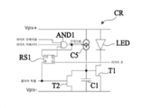
일 실시형태에 따르면, 유닛 CR은, 전위 Vpix+의 전극에 연결된 애노드와 MOS 트랜지스터(T1)의 드래인 또는 소스 중 한 제어 단자에 연결된 캐소드를 가지며 전위 Vpix-의 전극에 연결된 다른 제어 단자를 갖는 발광 다이오드(LED)를 구비한다. 유닛 CR은 트랜지스터(T1)의 게이트에 연결된 전극을 가지며 전위 Vpix-의 전극에 연결된 다른 전극을 갖는 커패시터(C1)을 더 구비한다. 유닛 CR은 트랜지스터(T1)의 게이트에 연결된 드래인 또는 소스 중 한 제어 단자를 가지며 전위 Vpix-의 전극에 연결된 다른 제어 단자를 갖는 MOS 트랜지스터(T2)를 더 구비한다. 트랜지스터(T2)의 게이트는 입력 클리어 픽셀에 연결된다. 유닛 CR은 유닛 CR의 입력 라이트 인에이블 및 라이트 커패시터에 대응하는 2개의 입력을 갖는 3-입력 AND 논리 게이트 AND1를 더 구비한다. 논리 게이트 AND1은, 전위 Vpix+의 전극에 연결된 단자와 트랜지스터(T1)의 게이트에 연결된 다른 단자를 갖는 전류 소스(CS)로 제어 신호 인에이블을 공급한다. 유닛 CR은 폴링 에지(falling edge)에 민감하며, 신호 인에이블을 수신하는 S 입력과, 유닛 CR의 입력 클리어 픽셀에 연결된 R 입력과, 논리 게이트 AND1의 제3 입력에 연결된 Q 출력을 갖는 RS 플립-플롭 RS1을 더 구비한다. 플립-플롭 RS1의 Q 출력은 유닛 CR의 출력 라이트돈에 연결된다.According to one embodiment, the unit CR has an anode connected to the electrode of the potential Vpix + and a cathode connected to one of the drain or source of the MOS transistor T1 and the other control terminal connected to the electrode of the potential Vpix-. A diode (LED) is provided. The unit CR further includes a capacitor C1 having an electrode connected to the gate of the transistor T1 and another electrode connected to the electrode of the potential Vpix-. The unit CR further includes a MOS transistor T2 having one control terminal of the drain or source connected to the gate of the transistor T1 and another control terminal connected to the electrode of the potential Vpix-. The gate of transistor T2 is connected to the input clear pixel. The unit CR further includes a 3-input AND logic gate AND1 having two inputs corresponding to the input light enable and write capacitor of the unit CR. The logic gate AND1 supplies control signal enable to a current source CS having a terminal connected to the electrode of the potential Vpix + and another terminal connected to the gate of the transistor T1. The unit CR is sensitive to a falling edge, an RS flip having an S input receiving signal enable, an R input connected to the input clear pixel of the unit CR, and a Q output connected to the third input of the logic gate AND1 -Flop RS1 is further provided. The Q output of the flip-flop RS1 is connected to the output lightdon of the unit CR.
도 17은 도 15의 표시 픽셀의 제어의 사이클 중 신호의 타이밍 다이어그램을 보여준다. 연속적인 시간을 to, t1, t2, t3, t4, t5, t6 및 t7이라 한다. 유닛 CR의 출력 라이트 인에이블은 신호 레드 돈(Red Done)을 공급한다. 유닛 CG의 출력 라이트 인에이블은 신호 그린 돈(Green Done)을 공급한다. 유닛 CB의 출력 라이트 인에이블은 신호 블루 돈(Blue Done)을 공급한다.FIG. 17 shows a timing diagram of the signal during the cycle of control of the display pixel of FIG. 15. The continuous time is called to, t1, t2, t3, t4, t5, t6 and t7. The output light enable of the unit CR supplies the signal Red Done. The unit CG's output light enable provides the signal Green Done. The output light enable of the unit CB supplies the signal Blue Done.
신호 레드 캡(Red Cap), 그린 캡(Green Cap), 및 블루 캡(Blue Cap) 각각은, 유닛 CR, CG 및 CB의 각각의 커패시터(C1)을 지나는 전압에 대응한다. 신호 sig는 전위 Vpix+와 Vpix- 사이의 차에 대응한다. 신호 sig는 3개의 이산값(discrete value) "0", "1" 및 "2"를 취할 수 있다.Each of the signal red cap, green cap, and blue cap corresponds to a voltage across each capacitor C1 of units CR, CG and CB. The signal sig corresponds to the difference between the potentials Vpix + and Vpix-. The signal sig can take three discrete values "0", "1" and "2".
본 실시형태에 있어서, 신호 데이터는 선택 단계 이외에는 신호 sig와 같고 신호 라이트는 표시 서브-픽셀의 제어 단계 중에는 "1"로 설정된다.In this embodiment, the signal data is the same as the signal sig except for the selection step, and the signal light is set to "1" during the control step of the display sub-pixel.
시간 t0에서, 신호 레드 돈, 그린 돈, 및 블루 돈은 "1"에 있고, 신호 sig는 "0"에 있으며, 신호 클리어는 "0"에 있다. 시간 t1에서는, 신호 sig가 "0"에서 "2"로 변환한다. 유닛 CM은 표시 픽셀이 선택되었는지를 검출하고 신호 클리어를 "1"로 설정한다. 시간 t2에서는, 신호 sig가 "0"으로 변환한다. 그러면, 유닛 CM은 신호 라이트를 "1"로 설정하고 신호 클리어를 "0"으로 설정한다. 이것은 유닛 CR, CG 및 CB의 플립-플롭 RS1을 초기화하고, 신호 레드 돈, 그린 돈, 및 블로 돈을 "0"으로 설정하고 유닛 CR, CG 및 CB의 커패시터 C1을 비워서, 전압 레드 캡, 그린 캡 및 블루 캡을 0으로 설정한다. 시간 t3에서, 적색 표시 서브-픽셀의 제어 단계를 시작한다. 본 실시형태에 있어서, 적색 표시 서브-픽셀이 활성화되고, 신호 sig는 "1"로 변환한다. 신호 데이터는 신호 sig와 같아서 유닛 CR의 커패시터 C1은, 신호 sig와 데이터가 "0"으로 변환되는 시간 t4까지 전류 소스 CS에 의하여 충전된다. 그러면 신호 레드 돈이 "1"로 변환된다. 시간 t5에서, 녹색 표시 서브-픽셀의 제어 단계가 시작된다. 본 실시형태에 있어서, 녹색 표시 서브-픽셀은 활성화되지 않고 매우 짧은 시간 동안 신호 sig가 "1"로 변환된다. 유닛 CG의 커패시터 C1은 실질적으로 충전되지 않으며 이때 신호 그린 돈이 "1"로 변환된다. 시간 t6에서는, 청색 표시 서브-픽셀의 제어 단계가 시작된다. 본 실시형태에 있어서, 청색 표시 서브-픽셀이 활성화되며 신호 sig "1"로 변환된다. 신호 데이트는 신호 sig와 같아서 유닛 CR의 커패시터 C1은 신호 sig와 데이터가 "0"으로 변환되는 시간 t7까지 전류 소스 CS에 의해 충전된다. 그런 후 신호 블루돈이 "1"로 변환된다.At time t0, the signal red money, green money, and blue money are at "1", the signal sig is at "0", and the signal clear is at "0". At time t1, the signal sig is converted from "0" to "2". The unit CM detects whether the display pixel is selected and sets the signal clear to "1". At time t2, the signal sig is converted to "0". Then, the unit CM sets the signal write to "1" and the signal clear to "0". This initializes the flip-flop RS1 of units CR, CG and CB, sets the signal red money, green money, and blow money to "0" and emptys capacitor C1 of units CR, CG and CB, voltage red cap, green Set the cap and blue cap to 0. At time t3, the control phase of the red display sub-pixel is started. In this embodiment, the red display sub-pixel is activated, and the signal sig converts to "1". The signal data is the same as the signal sig, so that the capacitor C1 of the unit CR is charged by the current source CS until time t4 when the signal sig and the data are converted to "0". The signal red money is then converted to "1". At time t5, the control phase of the green display sub-pixel is started. In this embodiment, the green indication sub-pixel is not activated and the signal sig is converted to "1" for a very short time. The capacitor C1 of the unit CG is not substantially charged, at which point the signal green money is converted to "1". At time t6, the control phase of the blue display sub-pixel is started. In this embodiment, the blue display sub-pixel is activated and converted to the signal sig "1". The signal date is equal to the signal sig so that the capacitor C1 of the unit CR is charged by the current source CS until time t7 when the signal sig and data are converted to "0". Then the signal bluedon is converted to "1".
도 18은, 예를 들어 이후에 설명되는 도 20에 도시된 전기 다이어그램에 대응하는 유닛 CG, 유닛 CR, CG의 출력 라이트와 예를 들어 이후에 설명되는 도 21에 도시된 전기 다이어그램에 대응하는 유닛 CB의 출력 라이트에 의하여 신호 엔드가 공급되는 경우에 적용된 유닛 CM의 다른 실시형태의 등가 전기 다이어그램을 보여준다. 본 실시형태에 있어서, 전송 단계 S2 중에, 신호 데이터는 임의의 지속시간 △T만큼 지연된 신호 sig와 동일하며 신호 라이트는 신호 sig와 동일하다.FIG. 18 shows, for example, output lights of units CG, unit CR, and CG corresponding to the electrical diagram shown in FIG. 20 described later, and units corresponding to the electrical diagram shown in FIG. 21 described later, for example. Shows an equivalent electrical diagram of another embodiment of the unit CM applied when the signal end is supplied by the output light of the CB. In the present embodiment, during the transmission step S2, the signal data is the same as the signal sig delayed by an arbitrary duration ΔT, and the signal write is the same as the signal sig.
유닛 CM은 전위 Vpix+의 전극에 연결된 입력 s+와 전위 Vpix-의 전극에 연결된 입력 s-를 구비하고 이진신호 스타트(start)를 제공하는 블록 스타트 검출기(block start detector)를 구비한다. 블록 스타트 검출기는 입력 s+ 및 s- 사이의 전압에 대응하는, 신호 sig가 "2"로 변환되는 것을 검출할 수 있고, 신호 sig가 "0"으로 다시 변환될 때 "1"로 신호 스타트를 설정할 수 있다.The unit CM has a block start detector having an input s + connected to the electrode of the potential Vpix + and an input s- connected to the electrode of the potential Vpix + and providing a binary signal start. The block start detector can detect that the signal sig is converted to "2", corresponding to the voltage between the inputs s + and s-, and sets the signal start to "1" when the signal sig is converted back to "0". You can.
유닛 CM은, 전위 Vpix+의 전극에 연결된 입력 s+와, 전위 Vpix-의 전극에 연결된 입력 s-와, 신호 스타트(start)를 수신하는 입력 인에이블(enable)을 구비하는 블록 데이터 추출기(block data extrator)를 구비한다. 이 블록은 신호 클리어와, 신호 sig로부터 추출되고, 예를 들어, 선택 단계 이외에서는 신호 sig의 이진수 버전에 대응하는 신호 로우_데이터(raw_data)를 제공한다.The unit CM is a block data extrator having an input s + connected to the electrode of the potential Vpix +, an input s- connected to the electrode of the potential Vpix +, and an input enable receiving a signal start. ). This block provides the signal raw and signal raw_data, which is extracted from the signal sig and corresponds to the binary version of the signal sig, for example, outside the selection phase.
유닛 CM은, 신호 로우-데이터를 수신하고 신호 로우_데이터와 동일한 신호 라이트(write)를 공급하며, 신호 데이터(data)를 공급하는 블록 제로 검출기(block zero detector)를 구비하며, 이 신호 데이터는, "1"에서의 각 펄스의 지속시간이 지속시간 △T만큼 감소되어 있는 신호 로우_데이터와 동일한 것으로, 각 펄스의 시작은 지속시간 △T만큼 지연되어 있고 각 펄스의 끝은 변경되지 않아서, 만일 신호 로우_데이터의 펄스가 지속시간 △T보다 짧으면, 신호 데이터는 대응하는 펄스를 구비하지 않는다.The unit CM is provided with a block zero detector that receives signal low-data, supplies the same signal write as signal low_data, and supplies signal data. , The duration of each pulse at "1" is the same as the signal row_data whose duration is reduced by the duration ΔT, and the start of each pulse is delayed by the duration △ T and the end of each pulse is not changed. If the pulse of the signal row_data is shorter than the duration ΔT, the signal data does not have a corresponding pulse.
도 19는 도 18에 도시된 유닛 CM의 일 실시형태의 좀 더 상세한 전기 다이어그램을 보여준다.FIG. 19 shows a more detailed electrical diagram of one embodiment of the unit CM shown in FIG. 18.
유닛 CM은, 전위 Vpix+의 전극과 전위 Vpix-의 전극 사이에 직렬-조립된 2개의 레지스터 R1 및 R2를 구비하는 제1 전압 분리 브리지를 구비한다. 제1 분리 브릿지의 중간 지점에는 2개의 인버터 INV1 및 INV2가 직렬로 연속하여 제공되며, 제2 인버터 INV2는 신호 스타트를 제공하고 있다. 유닛 CM은, 신호 스타트를 수신하는 S 입력과, 폴링 에지에 민감하며, 신호 엔드를 수신하는 입력 R을 갖는 RS 플립-플롭 RS2를 구비한다. 신호 엔드는, 도 20에서 설명되는 바와 같이, 유닛 CG의 출력 라이트 돈에 의하여 공급된다. 유닛 CM은, 신호 스타트를 수신하는 제1 입력과, 플립-플롭 RS2의 Q 출력에 연결된 제2 입력을 가지며 신호 인에이블을 제공하는 NOR 논리 게이트 NOR1을 구비한다.The unit CM has a first voltage separation bridge having two resistors R1 and R2 in series-assembled between the electrode of the potential Vpix + and the electrode of the potential Vpix-. At the intermediate point of the first separation bridge, two inverters INV1 and INV2 are provided in series, and the second inverter INV2 provides a signal start. The unit CM has an RS flip-flop RS2 having an S input for receiving a signal start and an input R sensitive for a falling edge and receiving a signal end. The signal end is supplied by the output light money of the unit CG, as described in FIG. 20. The unit CM has a first input for receiving a signal start, and a second input connected to the Q output of the flip-flop RS2 and a NOR logic gate NOR1 for providing signal enable.
유닛 CM은 전위 Vpix+의 전극과 전위 Vpix-의 전극 사이에 직렬-조립된 2개의 레지스터 R3 및 R4를 구비하는 제2 전압 분리 브리지를 구비한다. 유닛 CM은 전위 Vpix+의 전극과 전위 Vpix-의 전극 사이에 직렬 조립된 3개의 MOS 트랜지스터 T3, T4 및 T5를 구비한다. 트랜지스터 T3은 P채널을 가지며 트랜지스터 T4 및 T5는 N 채널을 갖는다. 트랜지스터 T3 및 T4의 게이트는 신호 인에이블을 수신한다. 제2 분리 브리지의 중간지점은 트랜지스터 T5의 게이트에 전력을 공급한다. The unit CM has a second voltage separation bridge having two resistors R3 and R4 in series-assembled between the electrode of the potential Vpix + and the electrode of the potential Vpix-. Unit CM has three MOS transistors T3, T4 and T5 assembled in series between the electrode of potential Vpix + and the electrode of potential Vpix-. Transistors T3 have P channels and transistors T4 and T5 have N channels. The gates of transistors T3 and T4 receive signal enable. The intermediate point of the second isolation bridge supplies power to the gate of transistor T5.
트랜지스터 T3의 소스는, 신호 라이트를 제공하는 인버터 INV3에 전력을 공급한다. 유닛 CM은, 신호 라이트를 수신하는 제1 입력을 갖는 2-입력 AND 논리 게이트 AND2를 구비한다. 유닛 CM은 인버터 INV3의 출력과 게이트 AND2의 제2 입력 사이에 조립된 레지스터 R5를 구비한다. 유닛 CM은 게이트 AND2의 제2 입력에 연결된 한 전극을 갖고, 전위 Vpix-의 전극에 연결된 다른 전극을 갖는 커패시터 C2를 구비한다. 게이트 AND2의 출력은 신호 데이터를 제공한다.The source of the transistor T3 supplies power to the inverter INV3, which provides signal light. The unit CM has a 2-input AND logic gate AND2 having a first input for receiving a signal write. Unit CM has a resistor R5 assembled between the output of inverter INV3 and the second input of gate AND2. Unit CM has a capacitor C2 having one electrode connected to the second input of gate AND2 and the other electrode connected to the electrode of potential Vpix-. The output of gate AND2 provides signal data.
도 20은 유닛 CR의 또 다른 실시형태의 등가 전기 다이어그램을 보여주며, 유닛 CG는 동일할 수 있다. 유닛 CR은 도 16에 도시된 유닛의 모든 소자를 구비하고 있으며, 플립-플롭 RS1의 S 입력이 유닛 CR의 입력 라이트 인에이블에 연결되어 있고, Q 신호를 수신하는 제1 입력을 갖고 입력 라이트 인에이블에 연결되어 있는 제2 입력을 가지며 출력 라이트 돈에 연결된 출력을 갖는 2-입력 AND 논리 게이트 AND3를 구비한다는 점에서 차이점을 갖는다. 20 shows an equivalent electrical diagram of another embodiment of the unit CR, and the unit CG may be the same. The unit CR is equipped with all the elements of the unit shown in FIG. 16, the S input of flip-flop RS1 is connected to the input light enable of the unit CR, and the input light in has a first input for receiving a Q signal. The difference is that it has a 2-input AND logic gate AND3 with a second input connected to the Able and an output connected to the output write money.
도 21은 유닛 CB의 다른 실시형태의 등가 전기 다이어그램을 보여준다. 유닛 CB는 도 16에 도시된 유닛의 모든 소자를 구비하고 있으나, 플립-플롭 RS1이 존재하지 않으며 3-입력 논리 게이트 AND1이, 유닛 CB의 입력 라이트 커패시터에 연결된 제1 입력을 가지며 유닛 CB의 입력 라이트 인에이블에 연결된 제2 입력을 갖고 신호 인에이블을 제공하는 2-입력 논리 게이트 AND4로 대체되어 있는 차이점을 갖는다. 21 shows an equivalent electrical diagram of another embodiment of the unit CB. Unit CB has all the elements of the unit shown in FIG. 16, but flip-flop RS1 is not present, and the 3-input logic gate AND1 has a first input connected to the input light capacitor of unit CB and has an input of unit CB. The difference is that it is replaced by a 2-input logic gate AND4, which has a second input connected to the light enable and provides signal enable.
도 22는 도 18의 표시 픽셀의 제어 사이클 동안의 신호의 타이밍 다이어그램을 보여준다. 연속적인 시간을 t'0. t'1. t'2, t'3, t'4, t'5, t'6, t'7, t'8 및 t'9라고 부른다. 신호 레드 라이트 인에이블(red write enable), 그린 라이트 인에이블(green write enable) 및 블루 라이트 인에이블(blue write enable)은 유닛 CR, CG, 및 CB이 입력 라이트 인에이블에 의하여 각각 수신된 신호에 대응한다.22 shows a timing diagram of a signal during a control cycle of the display pixel of FIG. 18. Continuous time t'0. t'1. It is called t'2, t'3, t'4, t'5, t'6, t'7, t'8 and t'9. Signals Red write enable, green write enable and blue write enable enable units CR, CG, and CB to respectively receive signals received by the input write enable. To respond.
신호는, t0, t1, 및 t2의 신호에 대하여 이미 설명했던 것과 동일한 방법으로 시간 t'0, t'1, t'2에서 변화한다. 시간 t'3에서, 적색 표시 서브-픽셀 제어 단계가 시작한다. 본 실시형태에 있어서, 적색 표시 서브-픽셀이 활성화되고 신호 sig는 "1"로 변환한다. 신호 데이터는 지속시간 △T만큼 지연된 신호 sig와 동일하며 따라서 유닛 CR의 커패시터 C1은 시간 t'4에서, 신호 sig, 데이터 및 레드 라이트 인에이블이 "0"으로 변환하는 시간 t'5까지 전류 소스 CS 에 의하여 충전된다. 이때 유닛 CR의 신호 라이트 돈은 신호 레드 라이트 인에이블과 동일하게 된다. 시간 t'6에서, 녹색 표시 서브-픽셀 제어 단계가 시작한다. 본 실시형태에서, 녹색 표시 서브-픽셀은 활성화되지 않으며 신호 sig는 △T보다 짧은 지속시간 동안 "1"로 변환한다. 신호 라이트 및 그린 라이트 인에이블도 또한 이 매우 짧은 지속시간 동안 "1"로 변환한다. 그러나, 신호 데이터는 "0"에서 유지되어서 유닛 CG의 커패시터 C는 충전되지 않는다. 그런 후 유닛 CR의 신호 라이트 돈이 신호 그린 라이트 인에이블과 동일하게 된다. 시간 t'7에서, 청색 표시 서브-픽셀 제어 단계가 시작한다. 본 실시형태에 있어서, 청색 표시 서브-픽셀이 활성화되며 신호 sig는 "1"로 변환한다. 신호 데이터는 지속시간 △T만큼 지연된 신호 sig와 동일하며 따라서 유닛 CB의 커패시터 C는 t'8에서 신호 sig, 데이터, 레드 라이트 인에이블, 그린 라이트 인에이블 및 블루 라이트 인에이블이 "0"으로 변환하는 시간 t'9까지 전류 소스 SC에 의하여 충전된다.The signals change at time t'0, t'1, t'2 in the same way as already described for the signals t0, t1, and t2. At time t'3, the red display sub-pixel control step begins. In this embodiment, the red display sub-pixel is activated and the signal sig converts to "1". The signal data is the same as the signal sig delayed by the duration ΔT, so the capacitor C1 of the unit CR is the current source from time t'4 to time t'5 where the signal sig, data and red light enable converts to "0" It is charged by CS. At this time, the signal light money of the unit CR is the same as the signal red light enable. At time t'6, the green display sub-pixel control step begins. In this embodiment, the green indication sub-pixel is not activated and the signal sig converts to "1" for a duration shorter than [Delta] T. Signal light and green light enable also convert to "1" for this very short duration. However, the signal data is maintained at "0" so that the capacitor C of the unit CG is not charged. The signal light money of the unit CR is then equal to the signal green light enable. At time t'7, the blue display sub-pixel control step begins. In this embodiment, the blue display sub-pixel is activated and the signal sig converts to "1". The signal data is the same as the signal sig delayed by the duration △ T, so the capacitor C in unit CB converts the signal sig, data, red light enable, green light enable and blue light enable to "0" at t'8. It is charged by the current source SC until time t'9.
일 실시형태에 따르면, 표시 픽셀은 150개의 MOS 트랜지스터, 5개의 레지스터 및 4개 커패시터보다 적게 형성될 수 있다. 따라서, 이것은 작은 표면 영역을 점유할 수 있다.According to one embodiment, the display pixel may be formed with less than 150 MOS transistors, 5 resistors, and 4 capacitors. Therefore, it can occupy a small surface area.
도 23은 표시 픽셀(Pix)의 또 다른 실시형태의 전기 다이어그램을 보여준다.23 shows an electrical diagram of another embodiment of a display pixel Pix.
표시 픽셀(Pix)은 전위 Vpix+에 있는 행 전극(102) 중 하나와 전위 Vpix-에 있는 열 전극(104) 중 하나에 연결되어 있다.The display pixel Pix is connected to one of the
표시 픽셀(Pix)은 레벨 검출 유닛 M1과 라이징 에지 검출기 M2 및 카운터 M3(링 카운터(Ring Counter)), 그리고 표시 서브-픽셀 제어 유닛 CR, CG, 및 CB를 구비한다. 유닛 M1, M2 및 M3의 전자 구성품은 제어 회로(20)의 레벨에 배치되어 있다. 유닛 CR, CG, CB의 전자 구성품은 제어 회로(20) 레벨 및/또는 광전자 회로(26) 레벨에 배치될 수 있다.The display pixel Pix has a level detection unit M1, a rising edge detector M2 and a counter M3 (Ring Counter), and a display sub-pixel control unit CR, CG, and CB. The electronic components of the units M1, M2 and M3 are arranged at the level of the
각 유닛 M1, M2, M3, CR, CG, 및 CB는, 그들 전기 전력 공급을 위한 전위 Vpix+ 및 Vpix-와 연결된 행 및 열 전극(102, 104)에 연결되어 있다. Each unit M1, M2, M3, CR, CG, and CB is connected to the row and
유닛 M1은 입력 V+ 및 V-에서 각각 입력 신호로서 전위값 Vpix+ 및 Vpix-와 이진 신호 리셋(Reset)을 수신하고 이진 신호 디텍트 인에이블(Detect Enable) 및 이진 신호 클리어를 제공한다. 유닛 M2는 입력 V+ 및 V-에서 각각 입력 신호로서 전위값 Vpix+ 및 Vpix- 및 입력 인에이블에서 이진 신호 디텍트 인에이블을 수신하고 이진 신호 클록을 제공한다. 유닛 M3은 이진 신호 클럭을 수신하고 3개의 이진 신호 b0, b1 및 b2를 제공한다. b2의 폴링 에지는 유닛 M1을 리셋한다.Unit M1 receives potential values Vpix + and Vpix- and binary signal reset as input signals at inputs V + and V-, respectively, and provides binary signal detect enable and binary signal clear. Unit M2 receives the binary signal detect enable at the potential values Vpix + and Vpix- and the input enable as input signals at inputs V + and V-, respectively, and provides a binary signal clock. Unit M3 receives the binary signal clock and provides three binary signals b0, b1 and b2. The falling edge of b2 resets unit M1.
각 유닛 CR, CG, 및 CB는 입력 캡 리셋(Cap Reset)과 입력 Prog를 구비한다. 각 유닛 CR, CG, 및 CB의 입력 캡 리셋은 신호 디텍트 인에이블을 수신한다. 유닛 CR의 입력 Prog는 신호 b0을 수신하고, 유닛 CG의 입력 Prog는 신호 b1을 수신하고, 유닛 CB의 입력 Prog는 신호 b2를 수신한다.Each unit CR, CG, and CB has an input cap reset and an input prog. The input cap reset of each unit CR, CG, and CB receives a signal detect enable. The input Prog of the unit CR receives the signal b0, the input Prog of the unit CG receives the signal b1, and the input Prog of the unit CB receives the signal b2.
본 실시형태에 있어서, 유닛 M1은, 표시 픽셀이 신호 sig의 증가에 의하여 선택되었는지를 검출할 수 있다. 선택이 검출되는 경우, 유닛 M2는 신호 sig의 라이징 에지를 검출한다. 유닛 CR, CG, 및 CB의 커패시터는 연속적으로 충전되며, 하나의 유닛에서 다른 유닛으로의 전환은 신호 sig의 폴링 에지에 의하여 트리거된다. 각 시퀀스의 초기에, 유닛 CR, CG, 및 CB의 커패시터가 방전된다.In this embodiment, the unit M1 can detect whether the display pixel has been selected by increasing the signal sig. If a selection is detected, unit M2 detects the rising edge of signal sig. The capacitors of units CR, CG, and CB are continuously charged, and the transition from one unit to another is triggered by the falling edge of signal sig. At the beginning of each sequence, the capacitors of units CR, CG, and CB are discharged.
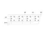
도 24는 유닛 M3의 실시형태를 보여준다. 유닛 M3은 비동기 /S 및 /R 입력을 갖는 일련의 4개의 D-형 플립-플롭 D1, D2, D3 및 D4를 구비한다. 각 플립-플롭 D1, D2 및 D3의 ck 입력은 신호 클럭을 수신한다. 플립-플롭 D1의 Q 출력은 플립-플롭 D2의 D 입력에 연결되고, 플립-플롭 D2의 Q 출력은 플립-플롭 D3의 D 입력에 연결되고, 플립-플롭 D3의 Q 출력은 플립-플롭 D4의 D 입력에 연결된다. 플립-플롭 D1의 출력은 카운터의 설정에서 "1"에 있으며, 동시에 다른 플립-플롭의 출력은 논리 상태 "0"에 있다. 비트 b0는 플립-플롭 D2의 Q 출력에 의하여 제공된 신호에 대응하며, 비트 b1은 플립-플롭 D3의 Q 출력에 의하여 제공된 신호에 대응하며, 비트 b2는 플립-플롭 D4의 Q 출력에 의하여 제공된 신호에 대응한다. 유닛 M1으로부터 발생된 신호 클리어는 인버터 INV9에 제공되며 플립-플롭 D1의 /S 입력뿐만 아니라 플립-플롭 D2, D3, 및 D4의 /R 입력에 전력을 공급한다.24 shows an embodiment of unit M3. Unit M3 has a series of four D-type flip-flops D1, D2, D3 and D4 with asynchronous / S and / R inputs. The ck input of each flip-flop D1, D2 and D3 receives the signal clock. The Q output of flip-flop D1 is connected to the D input of flip-flop D2, the Q output of flip-flop D2 is connected to the D input of flip-flop D3, and the Q output of flip-flop D3 is flip-flop D4 Is connected to the D input. The output of the flip-flop D1 is at "1" in the setting of the counter, while the output of the other flip-flop is at the logic state "0". Bit b0 corresponds to a signal provided by the Q output of flip-flop D2, bit b1 corresponds to a signal provided by Q output of flip-flop D3, and bit b2 is a signal provided by Q output of flip-flop D4 Corresponds to The signal clear generated from the unit M1 is provided to the inverter INV9 and supplies power to the / S input of flip-flop D1 as well as the / R input of flip-flop D2, D3, and D4.
도 25는 유닛 CR의 실시형태를 보여준다. 유닛 CG 및 CB는 동일한 구조를 가질 수 있다. 유닛 CR은 도 16에 도시된 유닛 CR과 동일한 구조를 가지며, 논리 게이트 AND1 및 플립-플롭 RS1이 존재하지 않고, 전류 소스 CS가 유닛 CR의 입력 Prog에 수신된 신호에 의하여 제어되고 트랜지스터 T2의 게이트가 유닛 CR의 입력 Cap_reset에서 수신된 신호에 의하여 제어된다는 차이점이 있다.25 shows an embodiment of the unit CR. Units CG and CB may have the same structure. The unit CR has the same structure as the unit CR shown in FIG. 16, there is no logic gate AND1 and flip-flop RS1, the current source CS is controlled by the signal received at the input Prog of the unit CR, and the gate of the transistor T2 The difference is that is controlled by the signal received at the input Cap_reset of the unit CR.
도 26은 도 23의 표시 픽셀의 제어 사이클 동안의 신호의 타이밍 다이어그램을 보여준다. 연속적인 시간을, t"0, t"1, t"2, t"3, t"4, t"5, t"6, t"7, t"8, t"9, t"10, t"11 및 t"12라 한다.FIG. 26 shows a timing diagram of the signal during the control cycle of the display pixel of FIG. 23. Continuous time, t "0, t" 1, t "2, t" 3, t "4, t" 5, t "6, t" 7, t "8, t" 9, t "10, t Referred to as "11 and t" 12.
시간 t"0에서, 신호 sig, 캡_리셋(Cap_reset), 디텍트 인에이블, 업(up), b0, b1, 및 b2는 "0"에 있다. 시간 t"1에서, 신호 sig는 "0"에서 "2"로 변환한다. 유닛 M1은 표시 픽셀이 선택되었는지를 검출하고 신호 클리어와 신호 디텍트 인에이블을 "1"로 설정한다. 시간 t"2에서, 신호 sig는 "1"로 변환하고 유닛 M1은 신호 클리어를 "0"으로 변환한다. 시간 t"3에서, 적색 표시 서브-픽셀 제어 단계 SR이 시작한다. 본 실시형태에 있어서, 적색 표시 서브-픽셀이 활성화되고 신호 sig가 "2"로 변환한다. 신호 클럭이 시간 t"3에서 시간 t"4까지 "1"로 설정된다. 신호 b0는 시간 t"3에서 "1"로 설정된다. 시간 t"5에서, 신호 sig는 "1"로 변환한다. 시간 t"6에서, 신호 sig는 "2"로 변환하고, 녹색 표시 서브-픽셀의 제어 단계 SG가 시작하면서 적색 서브-픽셀 제어 단계는 종료된다. 본 실시형태에서, 녹색 표시 서브-픽셀이 활성화된다. 신호 클럭이 시간 t"6에서 t"7까지 "1"로 설정된다. 신호 b1은 시간 t"6에서 "1"로 설정된다. 신호 b0는 시간 t"6에서 "0"으로 설정된다. 시간 t"8에서, 신호 sig는 "2"로 변환하고, 표시 서브-픽셀의 제어 단계 SB가 시작한다. 본 실시형태에 있어서, 청색 표시 서브-픽셀이 활성화된다. 신호 클럭이 시간 t"8에서 시간 t"9까지 "1"로 설정된다. 신호 b2는 시간 t"8에서 "1"로 설정된다. 신호 b1은 시간 t"8에서 "0"으로 설정된다. 시간 t"10에서, 신호 sig는 "1"로 변환한다. 시간 t"11에서, 신호 sig는 "2"로 설정된다. 이 처리의 종료가 통지된다. 시간 t"11에서, 신호 클럭은 "1"로 설정되며 신호 b2는 "0"으로 설정되고, 청색 서브-픽셀의 제어 단계 SB가 종료한다. 시간 t"12에서, 신호 sig는 "1"로 변환한 후 "0"으로 변환한다.At time t "0, the signal sig, Cap_reset, detect enable, up, b0, b1, and b2 are at" 0 ". At time t" 1, the signal sig is "0 Convert from "to" 2 ". Unit M1 detects whether the display pixel is selected and sets signal clear and signal detect enable to "1". At time t "2, the signal sig converts to" 1 "and the unit M1 converts signal clear to" 0 ". At time t" 3, the red indicator sub-pixel control step SR begins. In this embodiment, the red display sub-pixel is activated and the signal sig converts to "2". The signal clock is set to "1" from time t "3 to time t" 4. The signal b0 is set at time t "3 to" 1. "At time t" 5, the signal sig is converted to "1". At time t " 6, the signal sig is converted to " 2 ", and the red sub-pixel control step ends as the control step SG of the green display sub-pixel begins. The signal clock is set to "1" from time t "6 to t" 7. The signal b1 is set to time "1" at time t "6. The signal b0 is set to "0" at time t "6. At time t" 8, the signal sig is converted to "2", and the control step SB of the display sub-pixel starts. In this embodiment, the blue display sub-pixel is activated. The signal clock is set to "1" from time t "8 to time t" 9. Signal b2 is set to "1" at time t "8. Signal b1 is set to" 0 "at time t" 8. At time t "10, the signal sig is converted to" 1. "At time t" 11, the signal sig is set to "2". The end of this process is notified. At time t "11, the signal clock is set to" 1 "and the signal b2 is set to" 0 ", and the control step SB of the blue sub-pixel ends. At time t" 12, the signal sig is set to "1". After conversion, it is converted to "0".
일 실시형태에 따르면, 표시 픽셀은 150개의 MOS 트랜지스터, 3개의 레지스터, 및 4개의 커패시터보다 적게 하여 형성될 수 있다. 따라서, 적은 표면 영역을 차지할 수 있다.According to one embodiment, the display pixel may be formed with fewer than 150 MOS transistors, 3 resistors, and 4 capacitors. Therefore, it can occupy a small surface area.
데이터 이송 조건을 최적화하기 위하여, 모든 실시형태는 소통의 지속시간 동안 어드레스된 열 또는 행에서의 픽셀을 턴오프하는 기능을 탑재할 수 있으며, 이것은 데이터 전송 동안 구동되는 부하를 제한할 수 있다. 그런 기능성의 부가는 전위 차(Vpix+ - Vpix-)를 감소시킴으로써 실행할 수 있다.To optimize data transfer conditions, all embodiments can be equipped with the ability to turn off pixels in an addressed column or row for the duration of the communication, which can limit the load driven during data transfer. The addition of such functionality can be done by reducing the potential difference (Vpix +-Vpix-).
도 27a 내지 도 27h는, 도 1 및 도 2에 도시된 광전자 장치(10)를 제조하는 방법의 다른 실시형태의 연속적인 스텝으로 얻은 구조의 부분 개략 단면도이다.27A to 27H are partial schematic cross-sectional views of structures obtained by successive steps of another embodiment of the method of manufacturing the
도 27a는 복수의 소정의 제어 회로(20)를 구비하는 전자 회로(110)의 제조 후에 얻어진 구조를 보여주며, 도 27a에서는 예로서 4개의 제어 회로(20)가 도시되어 있다. 전자 회로(110)를 제조하는 방법은 집적 회로 제조 방법의 종래의 스텝을 구비할 수 있다.27A shows the structure obtained after manufacture of the
도 27b는 광전자 회로(26)를 전자 회로(110) 상에 부착한 후 얻어진 구조를 보여준다. 광전자 회로(26)를 전자 회로(110)에 조립하는 방법은 솔더링 작업을 구비할 수도 있다.27B shows the structure obtained after attaching the
도 27c는, 광전자 회로(26)와 광전자 회로(26) 사이에 있는 전자 회로(110)를 덮고 있는 전기적-절연층(112)을 증착한 후에 얻어진 구조를 보여준다. 절연층(112)은 이전에 설명된 절연부(28)와 동일한 재료로 이루어진다. 절연층(112)은, 화학기상증착(CVD), 플라즈마-강화 화학기상증착(PECV), 원자층 증착(ALD), 또는 캐소드 스퍼터링에 의하여 증착된 SiO2, SiN, Al2O3, ZrO2, HfO2, 또는 임의의 다른 유전 재료로 이루어질 수 있다.27C shows the structure obtained after depositing the electrically-insulating
도 27d는 절연층(112)에 도전성 소자(30)를 형성한 후 얻은 구조를 보여준다. 도전성 소자(30)는 절연층(112) 내의, 광전자 회로(26) 및/또는 제어 회로(20) 상에서 멈추는 개구를 에칭하고, 얻어진 구조물 전체 상에 도전층을 증착하고, 개구 외부의 도전층 부분을 제거함으로써 형성할 수 있다.27D shows the structure obtained after forming the
도 27e는, 표시 픽셀(Pix)을 획정하기 위하여 전기 회로(110)와 절연층(112)을 자른 후에 얻어진 구조를 보여준다. 27E shows the structure obtained after cutting the
도 27f는 지지대(12) 상에 이미 증착되어 있는 전극층(18)에 표시 픽셀(Pix)을 부착한 후에 얻은 구조를 보여준다. 예로서, 각 표시 픽셀(Pix)은, 분자 접착 또는 접착 재료, 특히 전기적-도전성 에폭시 글루를 통하여 전극층(18)에 부착할 수 있다.27F shows the structure obtained after attaching the display pixel Pix to the
도 27g는 표시 픽셀(Pix) 상에 그리고 표시 픽셀(Pix) 사이의 전극층(18) 상에 절연층(32)을 형성한 후에 얻은 구조를 보여준다. 절연층(32)은 SiO2, SiN, Al2O3, ZrO2, HfO2 또는 다른 유전체 재료일 수도 있다.27G shows the structure obtained after forming the insulating
도 27h는 각 표시 픽셀(Pix)의 상부로부터 절연층(32)을 제거한 후에 얻은 구조를 보여준다. 일 실시형태에 따르면, 그 제거는, 절연부(28) 상에서 정지하는 화학적-기계적 연마(CMP)에 의하여 수행될 수 있다. 또 다른 실시형태에 따르면, 이것은 절연층(32)의 화학적 에칭에 의하여 얻어질 수도 있다. 또 다른 실시형태에 따르면, 그 제거는, 절연층(32)의 증착 전에 각 표시 픽셀(Pix)의 상부에 희생층을 증착하고, 절연층(32)을 증착한 후에, 희생층과 희생층을 덮고 있는 절연층(32) 부분을 제거하는 것을 구비하는 소위 리프트-오프(lift-off) 방법에 의하여 수행될 수 있다.27H shows the structure obtained after removing the insulating
도 27i는 전극층(34)을 형성한 후 얻어진 구조를 보여준다. 전극층(34)은 CVD, PECVD, ALD, 캐소드 스퍼터링 또는 증기화에 의하여 증착된 TCO(투명 도전성 산화물)로 이루어질 수 있다.27I shows the structure obtained after forming the
도 28a 내지 도 28d는, 도 4b에 도시된 광전자 장치를 제조하는 방법의 또 다른 실시형태의 연속적인 스텝으로 얻어진 구조의 부분 개략 단면도이다.28A to 28D are partial schematic cross-sectional views of a structure obtained by successive steps of another embodiment of a method of manufacturing the optoelectronic device shown in FIG. 4B.
도 28a는, 복수의 광전자 회로(42)를 구비하는 광전자 회로(90)를 형성한 후에 얻은 구조를 보여주며, 도 27a에서는, 예로서, 3개의 광전자 회로(42)가 도시되어 있다. 예로서, 도 28a에서는, 각 광전자 회로(42)는 부분(47)에 의하여 분리된 2개의 광전자 회로(26)를 구비하는 것으로서 보여주고 있다.28A shows the structure obtained after forming the
도 28b는 광전자 회로(64)를 가로지르는 TSV(48)의 형성 후에 얻은 구조를 보여준다. 각 TSV(48)는 광전자 회로(90)를 가로지르는 개구를 에칭함으로써 형성될 수 있다. 이 개구는 원형 또는 사각형 단면적을 가질 수 있다. 에칭은 심도 반응성 이온 에칭(DRIE)일 수 있다. 그런 후 절연층이 개구의 벽에 증착된다. 절연층은, 예를 들어 PECVD에 의한 등각 증착 또는 절연성 폴리머의 등각 증착에 의하여 형성된다. 절연층은 10nm 내지 5,000nm의 범위, 예를 들어, 약 3㎛의 두께를 갖는다. 그런 후, TSV의 충전은 전해 구리 증착에 의하여 수행될 수 있다.28B shows the structure obtained after formation of
도 28c는 광전자 회로(90) 상에 절연층(92)의 증착 후에 얻은 구조를 보여준다. 절연층(92)은 이미 설명된 절연부(28)와 동일한 재료로 만들어진다. 절연층(92)은, CVD, PECVD, ALD, 또는 캐소드 스퍼터링에 의하여 증착될 수 있다.28C shows the structure obtained after deposition of the insulating
도 28d는, 절연층(92)에 도전성 소자(30)의 형성 후에 얻은 구조를 보여준다.28D shows the structure obtained after formation of the
이 방법의 이어지는 스텝은 도 27e 내지 도 27i와 관련하여 이미 설명된 것과 동일할 수 있다.Subsequent steps of this method may be the same as those already described with respect to FIGS. 27E-27I.
이상에서, 상이한 변형들을 갖는 다양한 실시형태를 기술하였다. 당업자들은 이들 다양한 실시형태의 다양한 소자와 임의의 발명 스텝에서 보여주지 않은 변형들을 결합할 수 있다. 예를 들어, 도 3에 도시된 전기 다이어그램은 도 4b에 도시된 장치(40)의 구조로 실행될 수 있으며 도 5에 도시된 전기 다이어그램은 도 1 및 도 2에 도시된 장치(10)의 구조로 실행될 수도 있다.In the above, various embodiments with different modifications have been described. Those skilled in the art can combine various elements of these various embodiments with variations not shown in any inventive step. For example, the electrical diagram shown in FIG. 3 can be implemented with the structure of the
Claims (16)
지지대(12)와,
상기 지지대를 덮고 있는 하나 이상의 제1 전기적-도전층(18)과,
상기 제1 전기적-도전층에 접착되어 있는 제1 및 제2 대향 표면(22, 23)을 구비하는 표시 픽셀 회로(Pix)로서, 각 표시 픽셀 회로는, 상기 제1 표면과 상기 제1 표면에 대향하는 제3 표면(24)을 구비하며 상기 제1 표면이 상기 제1 전기적-도전층에 접착되어 있는 전자 회로(20)와, 상기 제3 표면에 접착되어 있으며 하나 이상의 발광 다이오드(LED)를 구비하는 하나 이상의 광전자 회로(26; 42)를 구비하며, 상기 발광 다이오드의 전극들 중 하나 이상이 상기 제3 표면에 의해서 상기 전자 회로에 접속되어 있는, 표시 픽셀 회로(Pix)와,
상기 하나 이상의 표시 픽셀 회로를 덮고 있고 상기 제2 표면측에서 상기 하나 이상의 표시 픽셀 회로의 전자 회로에 전기적으로 연결되어 있는 하나 이상의 제2 전기적-도전층(34)
을 구비하는 광전자 장치.An optoelectronic device (10; 40; 50; 60; 70),
Support (12),
At least one first electrically-conductive layer 18 covering the support,
A display pixel circuit (Pix) having first and second opposing surfaces (22, 23) bonded to the first electrically-conductive layer, each display pixel circuit comprising: the first surface and the first surface An electronic circuit 20 having an opposing third surface 24 and having the first surface attached to the first electrically-conductive layer, and one or more light emitting diodes (LEDs) attached to the third surface. A display pixel circuit (Pix) having one or more optoelectronic circuits (26; 42), wherein at least one of the electrodes of the light emitting diode is connected to the electronic circuit by the third surface,
At least one second electro-conductive layer 34 covering the at least one display pixel circuit and electrically connected to the electronic circuit of the at least one display pixel circuit at the second surface side
Optoelectronic device having a.
상기 표시 픽셀 회로(Pix) 사이에서 상기 제1 전기적-도전층(18)을 덮고 있는 전기적-절연층(32)을 더 구비하는 광전자 장치.According to claim 1,
An optoelectronic device further comprising an electrically-insulating layer (32) covering the first electrically-conductive layer (18) between the display pixel circuits (Pix).
상기 전기적-절연층(32)은 상기 표시 픽셀 회로(Pix)의 측면을 덮고 있는 광전자 장치.According to claim 2,
The electrically-insulating layer 32 covers the side surface of the display pixel circuit Pix.
상기 하나 이상의 표시 픽셀 회로(Pix)는 전자 회로(20)와 광전자 회로(26;42)를 덮고 있는 전기적-절연부(28)를 더 구비하며, 하나 이상의 전기적-도전성 소자(30)가 상기 전기적-절연부를 가로질러 상기 제2 전기적 도전층(34) 및 상기 광전자 회로(26; 42) 또는 상기 전자 회로(20)에 연결되어 있는 광전자 장치.The method according to any one of claims 1 to 3,
The one or more display pixel circuits Pix further includes an electrical-insulating portion 28 covering the electronic circuit 20 and the optoelectronic circuits 26; 42, and the one or more electrical-conductive elements 30 are the electrical -Optoelectronic device connected to the second electrically conductive layer (34) and the optoelectronic circuit (26; 42) or the electronic circuit (20) across an insulating portion.
상기 하나 이상의 표시 픽셀 회로(Pix)에 대하여, 상기 광전자 회로(42)는 상기 광전자 회로의 나머지로부터 전기적으로 절연되어 있고 상기 전자 회로(20)와 상기 도전성 소자(30)에 전기적으로 연결되어 있는 관통 접속(48)을 구비하는 광전자 장치.According to claim 4,
For the one or more display pixel circuits Pix, the optoelectronic circuit 42 is electrically insulated from the rest of the optoelectronic circuit and is electrically connected to the electronic circuit 20 and the conductive element 30. Optoelectronic device having a connection (48).
상기 지지대(12)를 덮고 있는 2 이상의 분리된 제1 전기적-도전층(52)으로서, 상기 표시 픽셀 회로 중 제1 표시 픽셀 회로(Pix)가 각 제1 전기적-도전층에 부착되어 있는, 2 이상의 분리된 제1 전기적-도전층(52)과, 각각이, 상기 표시 픽셀 회로 중 제2 표시 픽셀 회로를 덮고 있으며 상기 제2 표시 픽셀 회로의 전자 회로(20)에 전기적으로 연결되어 있는 2 이상의 제2 전기적-도전층(34)을 구비하는 광전자 장치.The method according to any one of claims 1 to 5,
Two or more separate first electrically-conductive layers 52 covering the support 12, wherein a first display pixel circuit (Pix) of the display pixel circuits is attached to each first electrically-conductive layer, 2 Two or more separated first electrical-conductive layers 52, each covering the second display pixel circuit among the display pixel circuits and being electrically connected to the electronic circuit 20 of the second display pixel circuit An optoelectronic device comprising a second electrically-conductive layer (34).
상기 제1 전기적-도전층(18)과 상기 제2 전기적-도전층(34) 사이에, 제어 신호(COM)에 의하여 변조된 전압(VE)을 제공하는 유닛(unit)을 구비하고, 각 표시 픽셀 회로(Pix)의 전자 회로(20)는 상기 제어 신호를 추출하기 위하여 상기 전압을 복조할 수 있는 광전자 장치.The method according to any one of claims 1 to 5,
Between the first electrically-conductive layer 18 and the second electrically-conductive layer 34, there is provided a unit that provides a voltage (V E ) modulated by a control signal (COM), each An electronic circuit 20 of the display pixel circuit Pix is capable of demodulating the voltage to extract the control signal.
각 전자 회로(20)는 그 안에 저장된 식별자를 갖는 메모리를 구비하며, 상기 전자 회로에 저장된 상기 식별자들은 상이하며, 각 전자 회로(20)는 변조된 전압(VE)으로부터 상기 식별자 중 하나를 대표하는 정보를 추출할 수 있는 회로를 구비하는 광전자 장치.The method of claim 7,
Each electronic circuit 20 has a memory having an identifier stored therein, and the identifiers stored in the electronic circuit are different, and each electronic circuit 20 represents one of the identifiers from a modulated voltage V E An optoelectronic device having a circuit capable of extracting information to be performed.
상기 제2 전기적-도전층(34)에 통합 가능하며, 상기 표시 픽셀 회로(Pix)의 광전자 회로(26; 42)에 연결되어 있고, 전자기 방사선을 안내할 수 있는 하나 이상의 도파관(64)을 구비하는 광전자 장치.The method according to any one of claims 1 to 6,
One or more waveguides 64 that can be integrated into the second electro-conductive layer 34, are connected to the optoelectronic circuits 26; 42 of the display pixel circuit Pix, and are capable of guiding electromagnetic radiation. Optoelectronic device made.
상기 장치는 상기 도파관과 연결된 상기 전자기 방사선의 소스(68)를 더 구비하며, 각 표시 픽셀 회로(Pix)에 대하여, 상기 광전자 회로(26; 42)는, 측정 신호를 상기 전자 회로(20)로 공급할 수 있는 상기 전자기 방사선의 센서를 구비하는 광전자 장치.The method of claim 9,
The device further includes a source 68 of the electromagnetic radiation connected to the waveguide, and for each display pixel circuit Pix, the optoelectronic circuit 26; 42 sends a measurement signal to the electronic circuit 20. An optoelectronic device comprising the sensor of electromagnetic radiation that can be supplied.
상기 소스(68)는, 상기 전자기 방사선을 제어 신호(COM)로 변조할 수 있으며, 각 표시 픽셀 회로(Pix)에 대하여, 상기 전자 회로(20)는, 상기 제어 신호를 추출하기 위하여 상기 측정 신호를 복조할 수 있는 광전자 장치.The method of claim 10,
The source 68 may modulate the electromagnetic radiation into a control signal COM, and for each display pixel circuit Pix, the electronic circuit 20 may measure the measurement signal to extract the control signal. Optoelectronic device capable of demodulating.
상기 표시 픽셀 회로(Pix)의 다른 조합체들의 광전자 회로(26; 42)에 연결된, 제2 전기적-도전층(34)에 통합 가능한 2 이상의 도파관을 구비하는 광전자 장치.The method according to any one of claims 9 to 11,
An optoelectronic device having two or more waveguides integrating into a second electro-conductive layer (34) connected to optoelectronic circuits (26; 42) of different combinations of the display pixel circuit (Pix).
상기 도파관(64)과 상기 표시 픽셀 회로(Pix)의 적어도 일부 사이에 광학적 결합 수단(70)을 더 구비하는 광전자 장치.The method according to any one of claims 9 to 12,
And an optical coupling means (70) between the waveguide (64) and at least a portion of the display pixel circuit (Pix).
a) 제1 및 제2 대향 표면(22, 23)을 구비하는 표시 픽셀 회로(Pix)를 제조하는 스텝으로서, 각각은, 상기 제1 표면과 상기 제1 표면에 대향하는 제3 표면(24)을 구비하는 전자 회로(20)와, 상기 제3 표면에 접착되어 있으며 하나 이상의 발광 다이오드(LED)를 구비하는 하나 이상의 광전자 회로(26; 42)를 구비하며, 상기 발광 다이오드의 전극들 중 하나 이상이 상기 제3 표면에 의하여 상기 전자 회로에 접속되어 있는, 스텝과,
b) 하나 이상의 제1 전기적-도전층(18)으로 덮여 있는 지지대(12)를 제조하는 스텝과,
c) 상기 제1 전기적-도전층에 각 표시 픽셀 회로의 전자 회로(20)의 상기 제1 표면을 접착하는 스텝과,
d) 상기 하나 이상의 표시 픽셀 회로를 덮고 있으며, 상기 제2 표면측에서 상기 하나 이상의 표시 픽셀 회로의 상기 광전자 회로에 전기적으로 연결되어 있는 하나 이상의 제2 전기적-도전층(34)을 형성하는 스텝
을 구비하는 광전자 장치 제조 방법.A method of manufacturing an optoelectronic device (10; 40; 50; 60; 70),
a) a step of manufacturing a display pixel circuit (Pix) having first and second opposing surfaces (22, 23), each comprising: the first surface and a third surface (24) facing the first surface And an electronic circuit 20 having one or more optoelectronic circuits 26 and 42 attached to the third surface and having one or more light emitting diodes (LEDs), one or more of the electrodes of the light emitting diodes A step connected to the electronic circuit by the third surface;
b) manufacturing a support 12 covered with one or more first electrically-conductive layers 18,
c) bonding the first surface of the electronic circuit 20 of each display pixel circuit to the first electrically-conductive layer,
d) forming one or more second electro-conductive layers 34 covering the one or more display pixel circuits and electrically connected to the optoelectronic circuits of the one or more display pixel circuits on the second surface side
Method for manufacturing an optoelectronic device comprising a.
스텝 c)와 d) 사이에, 상기 표시 픽셀 회로(Pix) 사이에서 상기 제1 전기적-도전층(18)을 덮는 전기적-절연층(32)을 형성하는 스텝을 구비하는 광전자 장치 제조 방법.The method of claim 14,
And between step c) and d), forming an electrically-insulating layer 32 covering the first electrically-conductive layer 18 between the display pixel circuits Pix.
스텝 a)는, 상기 하나 이상의 표시 픽셀 회로(Pix)에 대하여, 상기 전자 회로(20)와 상기 광전자 회로(26; 42)를 덮는 전기적-절연부(18)와, 상기 전기적-절연부를 가로지르고 있으며 상기 제2 전기적-도전층(34)에 그리고 상기 광전자 회로(26; 42) 또는 상기 전자 회로(20)에 전기적으로 연결되어 있는 하나 이상의 전기적-도전성 소자(30)를 형성하는 것을 구비하는 광전자 장치 제조 방법.The method of claim 14 or 15,
Step a), for the one or more display pixel circuits (Pix), the electrical circuit 20 and the optoelectronic circuit (26; 42) covering the electrical-insulating portion (18), and crossing the electrical-insulating portion And forming one or more electrically-conductive elements 30 electrically connected to the second electrically-conductive layer 34 and to the optoelectronic circuit 26 or 42 or the electronic circuit 20. Device manufacturing method.
Applications Claiming Priority (3)
| Application Number | Priority Date | Filing Date | Title |
|---|---|---|---|
| FR1756984 | 2017-07-21 | ||
| FR1756984A FR3069378B1 (en) | 2017-07-21 | 2017-07-21 | OPTOELECTRONIC DEVICE |
| PCT/FR2018/051849 WO2019016481A1 (en) | 2017-07-21 | 2018-07-19 | Optoelectronic device |
Publications (2)
| Publication Number | Publication Date |
|---|---|
| KR20200033882A true KR20200033882A (en) | 2020-03-30 |
| KR102581705B1 KR102581705B1 (en) | 2023-09-21 |
Family
ID=60888466
Family Applications (1)
| Application Number | Title | Priority Date | Filing Date |
|---|---|---|---|
| KR1020207004028A Active KR102581705B1 (en) | 2017-07-21 | 2018-07-19 | optoelectronic devices |
Country Status (8)
| Country | Link |
|---|---|
| US (1) | US11522111B2 (en) |
| EP (1) | EP3655990B1 (en) |
| JP (1) | JP7146893B2 (en) |
| KR (1) | KR102581705B1 (en) |
| CN (1) | CN111108599B (en) |
| FR (1) | FR3069378B1 (en) |
| TW (1) | TWI768083B (en) |
| WO (1) | WO2019016481A1 (en) |
Cited By (3)
| Publication number | Priority date | Publication date | Assignee | Title |
|---|---|---|---|---|
| US11977808B2 (en) | 2020-08-13 | 2024-05-07 | Samsung Electronics Co., Ltd. | Display device |
| KR20240089498A (en) * | 2021-12-14 | 2024-06-20 | 알레디아 | Display pixels having light emitting diodes for display screens |
| US12505788B2 (en) | 2022-06-29 | 2025-12-23 | Aledia | Optoelectronic device |
Families Citing this family (11)
| Publication number | Priority date | Publication date | Assignee | Title |
|---|---|---|---|---|
| US11941114B1 (en) * | 2018-01-31 | 2024-03-26 | Vivint, Inc. | Deterrence techniques for security and automation systems |
| JP7231450B2 (en) * | 2019-03-18 | 2023-03-01 | ローム株式会社 | semiconductor light emitting device |
| JP7601771B2 (en) * | 2019-09-18 | 2024-12-17 | 泉州三安半導体科技有限公司 | Light Emitting Diode Package Assembly |
| FR3104795B1 (en) | 2019-12-12 | 2022-01-28 | Aledia | Device comprising a display screen with a low power operating mode |
| FR3112902B1 (en) | 2020-07-22 | 2022-12-16 | Aledia | Flexible optoelectronic device and method of making same |
| US11094846B1 (en) | 2020-08-31 | 2021-08-17 | 4233999 Canada Inc. | Monolithic nanocolumn structures |
| KR102747595B1 (en) | 2020-10-06 | 2024-12-27 | 엘지전자 주식회사 | Flat lighting device and display device using light-emitting elements |
| FR3127073B1 (en) * | 2021-09-13 | 2024-01-19 | Commissariat Energie Atomique | OPTOELECTRONIC DEVICE WITH SUPERIMPOSED EMISSIVE COMPONENTS AND PHOTODETECTOR |
| CN118339653B (en) * | 2021-11-26 | 2026-04-21 | 艾利迪公司 | Display pixels, including light-emitting diodes, are used for the display screen. |
| FR3137485B1 (en) * | 2022-06-29 | 2024-12-06 | Aledia | Display pixel comprising light-emitting sources |
| US11799054B1 (en) | 2023-02-08 | 2023-10-24 | 4233999 Canada Inc. | Monochromatic emitters on coalesced selective area growth nanocolumns |
Citations (4)
| Publication number | Priority date | Publication date | Assignee | Title |
|---|---|---|---|---|
| US6061039A (en) * | 1993-06-21 | 2000-05-09 | Ryan; Paul | Globally-addressable matrix of electronic circuit elements |
| US20110050658A1 (en) * | 2009-08-28 | 2011-03-03 | White Christopher J | Chiplet display with optical control |
| US20120256814A1 (en) * | 2011-04-08 | 2012-10-11 | Sony Corporation | Pixel chip, display panel, lighting panel, display unit, and lighting unit |
| KR20170059068A (en) * | 2015-11-19 | 2017-05-30 | 삼성전자주식회사 | Lighting source module, display panel and display apparatus |
Family Cites Families (9)
| Publication number | Priority date | Publication date | Assignee | Title |
|---|---|---|---|---|
| JP2002141492A (en) * | 2000-10-31 | 2002-05-17 | Canon Inc | Light emitting diode display panel and method of manufacturing the same |
| FR2995729B1 (en) | 2012-09-18 | 2016-01-01 | Aledia | SEMICONDUCTOR MICROFILL OR NANOWILE OPTOELECTRIC DEVICE AND METHOD FOR MANUFACTURING THE SAME |
| FR3011383B1 (en) | 2013-09-30 | 2017-05-26 | Commissariat Energie Atomique | METHOD FOR MANUFACTURING OPTOELECTRONIC DEVICES WITH ELECTROLUMINESCENT DIODES |
| JP2016167544A (en) * | 2015-03-10 | 2016-09-15 | ソニー株式会社 | Electronic component, electronic component mounting board and mounting method of electronic component |
| KR102402605B1 (en) * | 2015-07-28 | 2022-05-27 | 삼성디스플레이 주식회사 | organic light emitting display |
| FR3044467B1 (en) * | 2015-11-26 | 2018-08-10 | Commissariat A L'energie Atomique Et Aux Energies Alternatives | LIGHT DALLE AND METHOD FOR MANUFACTURING SUCH LIGHT SLAB |
| US9928771B2 (en) * | 2015-12-24 | 2018-03-27 | X-Celeprint Limited | Distributed pulse width modulation control |
| KR20170129983A (en) * | 2016-05-17 | 2017-11-28 | 삼성전자주식회사 | Led lighting device package, display apparatus using the same and method of manufacuring process the same |
| EP3491679B1 (en) * | 2016-07-26 | 2023-02-22 | CreeLED, Inc. | Light emitting diodes, components and related methods |
-
2017
- 2017-07-21 FR FR1756984A patent/FR3069378B1/en active Active
-
2018
- 2018-07-18 TW TW107124757A patent/TWI768083B/en active
- 2018-07-19 WO PCT/FR2018/051849 patent/WO2019016481A1/en not_active Ceased
- 2018-07-19 JP JP2020502940A patent/JP7146893B2/en active Active
- 2018-07-19 KR KR1020207004028A patent/KR102581705B1/en active Active
- 2018-07-19 CN CN201880061200.4A patent/CN111108599B/en active Active
- 2018-07-19 EP EP18762361.6A patent/EP3655990B1/en active Active
- 2018-07-19 US US16/631,806 patent/US11522111B2/en active Active
Patent Citations (4)
| Publication number | Priority date | Publication date | Assignee | Title |
|---|---|---|---|---|
| US6061039A (en) * | 1993-06-21 | 2000-05-09 | Ryan; Paul | Globally-addressable matrix of electronic circuit elements |
| US20110050658A1 (en) * | 2009-08-28 | 2011-03-03 | White Christopher J | Chiplet display with optical control |
| US20120256814A1 (en) * | 2011-04-08 | 2012-10-11 | Sony Corporation | Pixel chip, display panel, lighting panel, display unit, and lighting unit |
| KR20170059068A (en) * | 2015-11-19 | 2017-05-30 | 삼성전자주식회사 | Lighting source module, display panel and display apparatus |
Cited By (3)
| Publication number | Priority date | Publication date | Assignee | Title |
|---|---|---|---|---|
| US11977808B2 (en) | 2020-08-13 | 2024-05-07 | Samsung Electronics Co., Ltd. | Display device |
| KR20240089498A (en) * | 2021-12-14 | 2024-06-20 | 알레디아 | Display pixels having light emitting diodes for display screens |
| US12505788B2 (en) | 2022-06-29 | 2025-12-23 | Aledia | Optoelectronic device |
Also Published As
| Publication number | Publication date |
|---|---|
| CN111108599A (en) | 2020-05-05 |
| KR102581705B1 (en) | 2023-09-21 |
| JP2020527756A (en) | 2020-09-10 |
| EP3655990B1 (en) | 2024-11-27 |
| WO2019016481A1 (en) | 2019-01-24 |
| JP7146893B2 (en) | 2022-10-04 |
| CN111108599B (en) | 2023-10-13 |
| US20200161520A1 (en) | 2020-05-21 |
| FR3069378B1 (en) | 2019-08-23 |
| EP3655990A1 (en) | 2020-05-27 |
| FR3069378A1 (en) | 2019-01-25 |
| US11522111B2 (en) | 2022-12-06 |
| TWI768083B (en) | 2022-06-21 |
| TW201919201A (en) | 2019-05-16 |
Similar Documents
| Publication | Publication Date | Title |
|---|---|---|
| KR102581705B1 (en) | optoelectronic devices | |
| KR102550313B1 (en) | optoelectronic device | |
| EP3817079B1 (en) | Display panel, electronic device including same, and method for manufacturing display panel | |
| EP3565004B1 (en) | Display panel | |
| EP3072035B1 (en) | Display apparatus using semiconductor light emitting device | |
| CN110875365A (en) | Electronic equipment | |
| CN103460275A (en) | Electroluminescent display device with optical communication chiplet | |
| CN112335046B (en) | Optoelectronic devices including light emitting diodes | |
| CN107240598B (en) | Display panels, OLED modules and displays with touch functionality | |
| EP4672938A1 (en) | DISPLAY DEVICE AND ELECTRONIC DEVICE | |
| CN119230578A (en) | Display panel, display device, and method for manufacturing display panel |
Legal Events
| Date | Code | Title | Description |
|---|---|---|---|
| PA0105 | International application |
St.27 status event code: A-0-1-A10-A15-nap-PA0105 |
|
| PG1501 | Laying open of application |
St.27 status event code: A-1-1-Q10-Q12-nap-PG1501 |
|
| R18-X000 | Changes to party contact information recorded |
St.27 status event code: A-3-3-R10-R18-oth-X000 |
|
| A201 | Request for examination | ||
| PA0201 | Request for examination |
St.27 status event code: A-1-2-D10-D11-exm-PA0201 |
|
| D13-X000 | Search requested |
St.27 status event code: A-1-2-D10-D13-srh-X000 |
|
| D14-X000 | Search report completed |
St.27 status event code: A-1-2-D10-D14-srh-X000 |
|
| E902 | Notification of reason for refusal | ||
| PE0902 | Notice of grounds for rejection |
St.27 status event code: A-1-2-D10-D21-exm-PE0902 |
|
| AMND | Amendment | ||
| P11-X000 | Amendment of application requested |
St.27 status event code: A-2-2-P10-P11-nap-X000 |
|
| P13-X000 | Application amended |
St.27 status event code: A-2-2-P10-P13-nap-X000 |
|
| E601 | Decision to refuse application | ||
| PE0601 | Decision on rejection of patent |
St.27 status event code: N-2-6-B10-B15-exm-PE0601 |
|
| X091 | Application refused [patent] | ||
| AMND | Amendment | ||
| P11-X000 | Amendment of application requested |
St.27 status event code: A-2-2-P10-P11-nap-X000 |
|
| P13-X000 | Application amended |
St.27 status event code: A-2-2-P10-P13-nap-X000 |
|
| PX0901 | Re-examination |
St.27 status event code: A-2-3-E10-E12-rex-PX0901 |
|
| PX0701 | Decision of registration after re-examination |
St.27 status event code: A-3-4-F10-F13-rex-PX0701 |
|
| X701 | Decision to grant (after re-examination) | ||
| GRNT | Written decision to grant | ||
| PR0701 | Registration of establishment |
St.27 status event code: A-2-4-F10-F11-exm-PR0701 |
|
| PR1002 | Payment of registration fee |
St.27 status event code: A-2-2-U10-U12-oth-PR1002 Fee payment year number: 1 |
|
| PG1601 | Publication of registration |
St.27 status event code: A-4-4-Q10-Q13-nap-PG1601 |
|
| P22-X000 | Classification modified |
St.27 status event code: A-4-4-P10-P22-nap-X000 |
|
| R18 | Changes to party contact information recorded |
Free format text: ST27 STATUS EVENT CODE: A-5-5-R10-R18-OTH-X000 (AS PROVIDED BY THE NATIONAL OFFICE) |
|
| R18-X000 | Changes to party contact information recorded |
St.27 status event code: A-5-5-R10-R18-oth-X000 |
|
| P22-X000 | Classification modified |
St.27 status event code: A-4-4-P10-P22-nap-X000 |