KR20200034890A - 화소 및 이를 포함하는 표시 장치 - Google Patents
화소 및 이를 포함하는 표시 장치 Download PDFInfo
- Publication number
- KR20200034890A KR20200034890A KR1020180114287A KR20180114287A KR20200034890A KR 20200034890 A KR20200034890 A KR 20200034890A KR 1020180114287 A KR1020180114287 A KR 1020180114287A KR 20180114287 A KR20180114287 A KR 20180114287A KR 20200034890 A KR20200034890 A KR 20200034890A
- Authority
- KR
- South Korea
- Prior art keywords
- switching transistor
- gate
- electrode
- light sensing
- pixel
- Prior art date
- Legal status (The legal status is an assumption and is not a legal conclusion. Google has not performed a legal analysis and makes no representation as to the accuracy of the status listed.)
- Granted
Links
Images



Classifications
-
- G—PHYSICS
- G06—COMPUTING OR CALCULATING; COUNTING
- G06F—ELECTRIC DIGITAL DATA PROCESSING
- G06F3/00—Input arrangements for transferring data to be processed into a form capable of being handled by the computer; Output arrangements for transferring data from processing unit to output unit, e.g. interface arrangements
- G06F3/01—Input arrangements or combined input and output arrangements for interaction between user and computer
- G06F3/03—Arrangements for converting the position or the displacement of a member into a coded form
- G06F3/041—Digitisers, e.g. for touch screens or touch pads, characterised by the transducing means
- G06F3/0412—Digitisers structurally integrated in a display
-
- G—PHYSICS
- G09—EDUCATION; CRYPTOGRAPHY; DISPLAY; ADVERTISING; SEALS
- G09G—ARRANGEMENTS OR CIRCUITS FOR CONTROL OF INDICATING DEVICES USING STATIC MEANS TO PRESENT VARIABLE INFORMATION
- G09G3/00—Control arrangements or circuits, of interest only in connection with visual indicators other than cathode-ray tubes
- G09G3/20—Control arrangements or circuits, of interest only in connection with visual indicators other than cathode-ray tubes for presentation of an assembly of a number of characters, e.g. a page, by composing the assembly by combination of individual elements arranged in a matrix no fixed position being assigned to or needed to be assigned to the individual characters or partial characters
- G09G3/22—Control arrangements or circuits, of interest only in connection with visual indicators other than cathode-ray tubes for presentation of an assembly of a number of characters, e.g. a page, by composing the assembly by combination of individual elements arranged in a matrix no fixed position being assigned to or needed to be assigned to the individual characters or partial characters using controlled light sources
- G09G3/30—Control arrangements or circuits, of interest only in connection with visual indicators other than cathode-ray tubes for presentation of an assembly of a number of characters, e.g. a page, by composing the assembly by combination of individual elements arranged in a matrix no fixed position being assigned to or needed to be assigned to the individual characters or partial characters using controlled light sources using electroluminescent panels
- G09G3/32—Control arrangements or circuits, of interest only in connection with visual indicators other than cathode-ray tubes for presentation of an assembly of a number of characters, e.g. a page, by composing the assembly by combination of individual elements arranged in a matrix no fixed position being assigned to or needed to be assigned to the individual characters or partial characters using controlled light sources using electroluminescent panels semiconductive, e.g. using light-emitting diodes [LED]
- G09G3/3208—Control arrangements or circuits, of interest only in connection with visual indicators other than cathode-ray tubes for presentation of an assembly of a number of characters, e.g. a page, by composing the assembly by combination of individual elements arranged in a matrix no fixed position being assigned to or needed to be assigned to the individual characters or partial characters using controlled light sources using electroluminescent panels semiconductive, e.g. using light-emitting diodes [LED] organic, e.g. using organic light-emitting diodes [OLED]
- G09G3/3225—Control arrangements or circuits, of interest only in connection with visual indicators other than cathode-ray tubes for presentation of an assembly of a number of characters, e.g. a page, by composing the assembly by combination of individual elements arranged in a matrix no fixed position being assigned to or needed to be assigned to the individual characters or partial characters using controlled light sources using electroluminescent panels semiconductive, e.g. using light-emitting diodes [LED] organic, e.g. using organic light-emitting diodes [OLED] using an active matrix
- G09G3/3233—Control arrangements or circuits, of interest only in connection with visual indicators other than cathode-ray tubes for presentation of an assembly of a number of characters, e.g. a page, by composing the assembly by combination of individual elements arranged in a matrix no fixed position being assigned to or needed to be assigned to the individual characters or partial characters using controlled light sources using electroluminescent panels semiconductive, e.g. using light-emitting diodes [LED] organic, e.g. using organic light-emitting diodes [OLED] using an active matrix with pixel circuitry controlling the current through the light-emitting element
-
- G—PHYSICS
- G06—COMPUTING OR CALCULATING; COUNTING
- G06F—ELECTRIC DIGITAL DATA PROCESSING
- G06F3/00—Input arrangements for transferring data to be processed into a form capable of being handled by the computer; Output arrangements for transferring data from processing unit to output unit, e.g. interface arrangements
- G06F3/01—Input arrangements or combined input and output arrangements for interaction between user and computer
- G06F3/03—Arrangements for converting the position or the displacement of a member into a coded form
- G06F3/041—Digitisers, e.g. for touch screens or touch pads, characterised by the transducing means
- G06F3/0416—Control or interface arrangements specially adapted for digitisers
-
- G—PHYSICS
- G06—COMPUTING OR CALCULATING; COUNTING
- G06F—ELECTRIC DIGITAL DATA PROCESSING
- G06F3/00—Input arrangements for transferring data to be processed into a form capable of being handled by the computer; Output arrangements for transferring data from processing unit to output unit, e.g. interface arrangements
- G06F3/01—Input arrangements or combined input and output arrangements for interaction between user and computer
- G06F3/03—Arrangements for converting the position or the displacement of a member into a coded form
- G06F3/041—Digitisers, e.g. for touch screens or touch pads, characterised by the transducing means
- G06F3/0416—Control or interface arrangements specially adapted for digitisers
- G06F3/0418—Control or interface arrangements specially adapted for digitisers for error correction or compensation, e.g. based on parallax, calibration or alignment
-
- G—PHYSICS
- G06—COMPUTING OR CALCULATING; COUNTING
- G06F—ELECTRIC DIGITAL DATA PROCESSING
- G06F3/00—Input arrangements for transferring data to be processed into a form capable of being handled by the computer; Output arrangements for transferring data from processing unit to output unit, e.g. interface arrangements
- G06F3/01—Input arrangements or combined input and output arrangements for interaction between user and computer
- G06F3/03—Arrangements for converting the position or the displacement of a member into a coded form
- G06F3/041—Digitisers, e.g. for touch screens or touch pads, characterised by the transducing means
- G06F3/042—Digitisers, e.g. for touch screens or touch pads, characterised by the transducing means by opto-electronic means
-
- G—PHYSICS
- G06—COMPUTING OR CALCULATING; COUNTING
- G06F—ELECTRIC DIGITAL DATA PROCESSING
- G06F3/00—Input arrangements for transferring data to be processed into a form capable of being handled by the computer; Output arrangements for transferring data from processing unit to output unit, e.g. interface arrangements
- G06F3/01—Input arrangements or combined input and output arrangements for interaction between user and computer
- G06F3/03—Arrangements for converting the position or the displacement of a member into a coded form
- G06F3/041—Digitisers, e.g. for touch screens or touch pads, characterised by the transducing means
- G06F3/042—Digitisers, e.g. for touch screens or touch pads, characterised by the transducing means by opto-electronic means
- G06F3/0421—Digitisers, e.g. for touch screens or touch pads, characterised by the transducing means by opto-electronic means by interrupting or reflecting a light beam, e.g. optical touch-screen
-
- G06K9/00006—
-
- G—PHYSICS
- G06—COMPUTING OR CALCULATING; COUNTING
- G06V—IMAGE OR VIDEO RECOGNITION OR UNDERSTANDING
- G06V40/00—Recognition of biometric, human-related or animal-related patterns in image or video data
- G06V40/10—Human or animal bodies, e.g. vehicle occupants or pedestrians; Body parts, e.g. hands
- G06V40/12—Fingerprints or palmprints
-
- G—PHYSICS
- G06—COMPUTING OR CALCULATING; COUNTING
- G06V—IMAGE OR VIDEO RECOGNITION OR UNDERSTANDING
- G06V40/00—Recognition of biometric, human-related or animal-related patterns in image or video data
- G06V40/10—Human or animal bodies, e.g. vehicle occupants or pedestrians; Body parts, e.g. hands
- G06V40/12—Fingerprints or palmprints
- G06V40/13—Sensors therefor
- G06V40/1318—Sensors therefor using electro-optical elements or layers, e.g. electroluminescent sensing
-
- G—PHYSICS
- G06—COMPUTING OR CALCULATING; COUNTING
- G06V—IMAGE OR VIDEO RECOGNITION OR UNDERSTANDING
- G06V40/00—Recognition of biometric, human-related or animal-related patterns in image or video data
- G06V40/10—Human or animal bodies, e.g. vehicle occupants or pedestrians; Body parts, e.g. hands
- G06V40/12—Fingerprints or palmprints
- G06V40/1347—Preprocessing; Feature extraction
- G06V40/1359—Extracting features related to ridge properties; Determining the fingerprint type, e.g. whorl or loop
-
- G—PHYSICS
- G09—EDUCATION; CRYPTOGRAPHY; DISPLAY; ADVERTISING; SEALS
- G09G—ARRANGEMENTS OR CIRCUITS FOR CONTROL OF INDICATING DEVICES USING STATIC MEANS TO PRESENT VARIABLE INFORMATION
- G09G3/00—Control arrangements or circuits, of interest only in connection with visual indicators other than cathode-ray tubes
- G09G3/20—Control arrangements or circuits, of interest only in connection with visual indicators other than cathode-ray tubes for presentation of an assembly of a number of characters, e.g. a page, by composing the assembly by combination of individual elements arranged in a matrix no fixed position being assigned to or needed to be assigned to the individual characters or partial characters
- G09G3/22—Control arrangements or circuits, of interest only in connection with visual indicators other than cathode-ray tubes for presentation of an assembly of a number of characters, e.g. a page, by composing the assembly by combination of individual elements arranged in a matrix no fixed position being assigned to or needed to be assigned to the individual characters or partial characters using controlled light sources
- G09G3/30—Control arrangements or circuits, of interest only in connection with visual indicators other than cathode-ray tubes for presentation of an assembly of a number of characters, e.g. a page, by composing the assembly by combination of individual elements arranged in a matrix no fixed position being assigned to or needed to be assigned to the individual characters or partial characters using controlled light sources using electroluminescent panels
- G09G3/32—Control arrangements or circuits, of interest only in connection with visual indicators other than cathode-ray tubes for presentation of an assembly of a number of characters, e.g. a page, by composing the assembly by combination of individual elements arranged in a matrix no fixed position being assigned to or needed to be assigned to the individual characters or partial characters using controlled light sources using electroluminescent panels semiconductive, e.g. using light-emitting diodes [LED]
- G09G3/3208—Control arrangements or circuits, of interest only in connection with visual indicators other than cathode-ray tubes for presentation of an assembly of a number of characters, e.g. a page, by composing the assembly by combination of individual elements arranged in a matrix no fixed position being assigned to or needed to be assigned to the individual characters or partial characters using controlled light sources using electroluminescent panels semiconductive, e.g. using light-emitting diodes [LED] organic, e.g. using organic light-emitting diodes [OLED]
- G09G3/3266—Details of drivers for scan electrodes
-
- G—PHYSICS
- G09—EDUCATION; CRYPTOGRAPHY; DISPLAY; ADVERTISING; SEALS
- G09G—ARRANGEMENTS OR CIRCUITS FOR CONTROL OF INDICATING DEVICES USING STATIC MEANS TO PRESENT VARIABLE INFORMATION
- G09G3/00—Control arrangements or circuits, of interest only in connection with visual indicators other than cathode-ray tubes
- G09G3/20—Control arrangements or circuits, of interest only in connection with visual indicators other than cathode-ray tubes for presentation of an assembly of a number of characters, e.g. a page, by composing the assembly by combination of individual elements arranged in a matrix no fixed position being assigned to or needed to be assigned to the individual characters or partial characters
- G09G3/22—Control arrangements or circuits, of interest only in connection with visual indicators other than cathode-ray tubes for presentation of an assembly of a number of characters, e.g. a page, by composing the assembly by combination of individual elements arranged in a matrix no fixed position being assigned to or needed to be assigned to the individual characters or partial characters using controlled light sources
- G09G3/30—Control arrangements or circuits, of interest only in connection with visual indicators other than cathode-ray tubes for presentation of an assembly of a number of characters, e.g. a page, by composing the assembly by combination of individual elements arranged in a matrix no fixed position being assigned to or needed to be assigned to the individual characters or partial characters using controlled light sources using electroluminescent panels
- G09G3/32—Control arrangements or circuits, of interest only in connection with visual indicators other than cathode-ray tubes for presentation of an assembly of a number of characters, e.g. a page, by composing the assembly by combination of individual elements arranged in a matrix no fixed position being assigned to or needed to be assigned to the individual characters or partial characters using controlled light sources using electroluminescent panels semiconductive, e.g. using light-emitting diodes [LED]
- G09G3/3208—Control arrangements or circuits, of interest only in connection with visual indicators other than cathode-ray tubes for presentation of an assembly of a number of characters, e.g. a page, by composing the assembly by combination of individual elements arranged in a matrix no fixed position being assigned to or needed to be assigned to the individual characters or partial characters using controlled light sources using electroluminescent panels semiconductive, e.g. using light-emitting diodes [LED] organic, e.g. using organic light-emitting diodes [OLED]
- G09G3/3275—Details of drivers for data electrodes
-
- G—PHYSICS
- G09—EDUCATION; CRYPTOGRAPHY; DISPLAY; ADVERTISING; SEALS
- G09G—ARRANGEMENTS OR CIRCUITS FOR CONTROL OF INDICATING DEVICES USING STATIC MEANS TO PRESENT VARIABLE INFORMATION
- G09G2300/00—Aspects of the constitution of display devices
- G09G2300/08—Active matrix structure, i.e. with use of active elements, inclusive of non-linear two terminal elements, in the pixels together with light emitting or modulating elements
- G09G2300/0809—Several active elements per pixel in active matrix panels
-
- G—PHYSICS
- G09—EDUCATION; CRYPTOGRAPHY; DISPLAY; ADVERTISING; SEALS
- G09G—ARRANGEMENTS OR CIRCUITS FOR CONTROL OF INDICATING DEVICES USING STATIC MEANS TO PRESENT VARIABLE INFORMATION
- G09G2360/00—Aspects of the architecture of display systems
- G09G2360/14—Detecting light within display terminals, e.g. using a single or a plurality of photosensors
Landscapes
- Engineering & Computer Science (AREA)
- Theoretical Computer Science (AREA)
- Physics & Mathematics (AREA)
- General Physics & Mathematics (AREA)
- General Engineering & Computer Science (AREA)
- Human Computer Interaction (AREA)
- Computer Hardware Design (AREA)
- Multimedia (AREA)
- Computer Vision & Pattern Recognition (AREA)
- Control Of Indicators Other Than Cathode Ray Tubes (AREA)
- Control Of El Displays (AREA)
- Electroluminescent Light Sources (AREA)
Abstract
Description
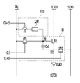
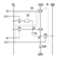
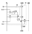
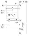
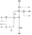
도 2a 및 도 2b는 본 발명에 따른 화소를 나타낸 회로도이다.
도 3은 본 발명에 따른 광 센싱 소자의 전류 특성 변화를 나타내는 그래프이다.
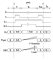
도 4는 본 발명의 화소의 구동을 설명하기 위한 타이밍도이다.
도 5는 본 발명의 제1 실시 예에 따른 화소를 나타낸 회로도이다.
도 6은 본 발명의 제2 실시 예에 따른 화소를 나타낸 회로도이다.
도 7은 본 발명의 제3 실시 예에 따른 화소를 나타낸 회로도이다.
도 8은 본 발명의 제4 실시 예에 따른 화소를 나타낸 회로도이다.
도 9는 본 발명의 제5 실시 예에 따른 화소를 나타낸 회로도이다.
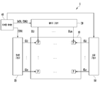
P: 화소
10: 표시 패널
20: 게이트 구동부
30: 데이터 구동부
40: 타이밍 제어부
50: 발광 구동부
Claims (19)
- 데이터 라인으로부터의 데이터 신호에 대응하여 유기 발광 다이오드로 공급되는 전류량을 제어하는 화소 회로; 및
상기 데이터 라인과 상기 화소 회로 사이에 연결되며, 입사광에 대응하여 상기 화소 회로로 공급되는 전류량을 제어하는 광 센서 회로를 포함하는 것을 특징으로 하는 화소. - 제1항에 있어서, 상기 광 센서 회로는,
상기 데이터 라인에 연결되는 광 센싱 스위칭 트랜지스터; 및
상기 광 센싱 스위칭 트랜지스터와 상기 화소 회로에 포함되는 구동 트랜지스터의 게이트 전극 사이에 연결되는 광 센싱 소자를 포함하는 것을 특징으로 하는 화소. - 제2항에 있어서, 상기 광 센싱 소자는,
상기 입사광에 대응하는 전류를 상기 구동 트랜지스터로 출력하는 것을 특징으로 하는 화소. - 제3항에 있어서, 상기 광 센싱 소자는,
비정질 실리콘 박막 트랜지스터인 것을 특징으로 하는 화소. - 제3항에 있어서, 상기 광 센싱 소자는,
상기 광 센싱 스위칭 트랜지스터에 연결되는 제1 전극;
상기 구동 트랜지스터의 상기 게이트 전극에 연결되는 제2 전극; 및
상기 광 센싱 소자의 상기 제1 전극 또는 상기 제2 전극과 연결되는 게이트 전극을 포함하는 것을 특징으로 하는 화소. - 제2항에 있어서, 상기 광 센싱 스위칭 트랜지스터는,
제1 게이트 라인을 통해 제1 게이트 신호가 인가됨에 따라 턴-온되어 상기 데이터 라인과 상기 광 센싱 소자를 전기적으로 연결시키는 것을 특징으로 하는 화소. - 제6항에 있어서, 상기 화소 회로는,
상기 구동 트랜지스터;
상기 구동 트랜지스터의 상기 게이트 전극과 상기 데이터 라인 사이에 연결되는 제1 스위칭 트랜지스터;
상기 유기 발광 다이오드와 센싱 라인 사이에 연결되는 제2 스위칭 트랜지스터; 및
상기 구동 트랜지스터의 상기 게이트 전극과 상기 제2 스위칭 트랜지스터 사이에 연결되는 커패시터를 포함하는 것을 특징으로 하는 화소. - 제7항에 있어서, 상기 제1 스위칭 트랜지스터는,
제2 게이트 라인을 통해 제2 게이트 신호가 공급됨에 따라 턴-온되고,
상기 제2 스위칭 트랜지스터는,
제3 게이트 라인을 통해 제3 게이트 신호가 공급됨에 따라 턴-온되는 것을 특징으로 하는 화소. - 제8항에 있어서,
상기 제2 스위칭 트랜지스터가 턴-온되는 동안 상기 제1 스위칭 트랜지스터 및 상기 광 센싱 스위칭 트랜지스터는 상이한 구간에서 적어도 1회 턴-온되는 것을 특징으로 하는 화소. - 제8항에 있어서,
상기 광 센싱 스위칭 트랜지스터 및 상기 제2 스위칭 트랜지스터가 턴-온될 때, 상기 광 센싱 소자로부터 상기 화소 회로로 공급되는 전류량에 대응하여 상기 센싱 라인의 전압 또는 전류 중 적어도 하나가 제어되는 것을 특징으로 하는 화소. - 게이트 라인들 및 데이터 라인들과 연결되는 복수의 화소들;
상기 게이트 라인들로 게이트 신호를 제공하는 게이트 구동부;
상기 데이터 라인들로 데이터 신호를 제공하는 데이터 구동부; 및
상기 게이트 구동부와 상기 데이터 구동부를 제어하는 타이밍 제어부를 포함하되,
상기 복수의 화소들 각각은,
데이터 라인으로부터의 데이터 신호에 대응하여 유기 발광 다이오드로 공급되는 전류량을 제어하기 위한 화소 회로; 및
상기 데이터 라인과 상기 화소 회로 사이에 연결되며, 입사광에 대응하여 상기 화소 회로로 공급되는 전류량을 제어하는 광 센서 회로를 포함하고,
상기 타이밍 제어부는,
상기 전류량에 대응하여 터치 입력 또는 지문을 감지하는 것을 특징으로 하는 표시 장치. - 제11항에 있어서, 상기 광 센서 회로는,
상기 데이터 라인에 연결되는 광 센싱 스위칭 트랜지스터; 및
상기 광 센싱 스위칭 트랜지스터와 상기 화소 회로에 포함되는 구동 트랜지스터의 게이트 전극 사이에 연결되는 광 센싱 소자를 포함하는 것을 특징으로 하는 표시 장치. - 제12항에 있어서, 상기 광 센싱 소자는,
상기 광 센싱 스위칭 트랜지스터에 연결되는 제1 전극;
상기 구동 트랜지스터의 상기 게이트 전극에 연결되는 제2 전극; 및
상기 광 센싱 소자의 상기 제1 전극 또는 상기 제2 전극과 연결되는 게이트 전극을 포함하는 것을 특징으로 하는 표시 장치. - 제13항에 있어서, 상기 화소 회로는,
상기 구동 트랜지스터;
상기 구동 트랜지스터의 상기 게이트 전극과 상기 데이터 라인 사이에 연결되는 제1 스위칭 트랜지스터;
상기 유기 발광 다이오드와 센싱 라인 사이에 연결되는 제2 스위칭 트랜지스터; 및
상기 구동 트랜지스터의 상기 게이트 전극과 상기 제2 스위칭 트랜지스터 사이에 연결되는 커패시터를 포함하는 것을 특징으로 하는 표시 장치. - 제14항에 있어서, 상기 광 센싱 스위칭 트랜지스터는,
제1 게이트 라인에 연결되고,
상기 제1 스위칭 트랜지스터는,
제2 게이트 라인에 연결되며,
상기 제2 스위칭 트랜지스터는,
제3 게이트 라인에 연결되는 것을 특징으로 하는 표시 장치. - 제15항에 있어서,
상기 제3 게이트 라인으로 제3 게이트 신호가 공급되는 동안, 상기 제1 게이트 라인 및 상기 제2 게이트 라인으로 제1 게이트 신호 및 제2 게이트 신호가 각각 적어도 1회 공급되되, 상기 제1 게이트 신호 및 상기 제2 게이트 신호는 상이한 구간에서 공급되는 것을 특징으로 하는 표시 장치. - 제16항에 있어서, 상기 제1 스위칭 트랜지스터는,
상기 제2 게이트 신호가 공급되는 초기화 구간 동안, 상기 데이터 라인으로 인가되는 제1 기준 전압을 상기 구동 트랜지스터의 상기 게이트 전극으로 공급하고,
상기 제2 스위칭 트랜지스터는,
상기 초기화 구간 동안, 상기 센싱 라인으로 공급되는 초기화 전압을 상기 구동 트랜지스터와 상기 유기 발광 다이오드의 공통 노드로 공급하는 것을 특징으로 하는 표시 장치. - 제17항에 있어서,
상기 초기화 구간 동안 상기 구동 트랜지스터의 구동 전압은 상기 제1 기준 전압 및 상기 초기화 전압 차이에 대응하는 전압으로 초기화되는 것을 특징으로 하는 표시 장치. - 제17항에 있어서, 상기 광 센싱 스위칭 트랜지스터는,
상기 제1 게이트 신호가 공급되는 센싱 구간 동안, 상기 데이터 라인으로 인가되는 제2 기준 전압을 상기 광 센싱 소자로 공급하는 것을 특징으로 하는 표시 장치.
Priority Applications (4)
| Application Number | Priority Date | Filing Date | Title |
|---|---|---|---|
| KR1020180114287A KR102542606B1 (ko) | 2018-09-21 | 2018-09-21 | 화소 및 이를 포함하는 표시 장치 |
| US16/567,705 US11087679B2 (en) | 2018-09-21 | 2019-09-11 | Pixel and display device including the same |
| CN201910885297.7A CN110941359B (zh) | 2018-09-21 | 2019-09-19 | 像素和包括该像素的显示装置 |
| EP19198467.3A EP3627295B1 (en) | 2018-09-21 | 2019-09-19 | Pixel and display device including the same |
Applications Claiming Priority (1)
| Application Number | Priority Date | Filing Date | Title |
|---|---|---|---|
| KR1020180114287A KR102542606B1 (ko) | 2018-09-21 | 2018-09-21 | 화소 및 이를 포함하는 표시 장치 |
Publications (2)
| Publication Number | Publication Date |
|---|---|
| KR20200034890A true KR20200034890A (ko) | 2020-04-01 |
| KR102542606B1 KR102542606B1 (ko) | 2023-06-15 |
Family
ID=67998211
Family Applications (1)
| Application Number | Title | Priority Date | Filing Date |
|---|---|---|---|
| KR1020180114287A Active KR102542606B1 (ko) | 2018-09-21 | 2018-09-21 | 화소 및 이를 포함하는 표시 장치 |
Country Status (4)
| Country | Link |
|---|---|
| US (1) | US11087679B2 (ko) |
| EP (1) | EP3627295B1 (ko) |
| KR (1) | KR102542606B1 (ko) |
| CN (1) | CN110941359B (ko) |
Cited By (3)
| Publication number | Priority date | Publication date | Assignee | Title |
|---|---|---|---|---|
| US11955078B2 (en) | 2021-09-29 | 2024-04-09 | Samsung Display Co., Ltd. | Display device |
| US12213357B2 (en) | 2021-09-29 | 2025-01-28 | Samsung Display Co., Ltd. | Display device |
| US12293714B2 (en) | 2022-04-25 | 2025-05-06 | Samsung Display Co., Ltd. | Display device |
Families Citing this family (8)
| Publication number | Priority date | Publication date | Assignee | Title |
|---|---|---|---|---|
| WO2021220141A1 (ja) * | 2020-05-01 | 2021-11-04 | 株式会社半導体エネルギー研究所 | 表示装置、表示モジュール、及び電子機器 |
| CN112287845B (zh) * | 2020-10-30 | 2022-09-27 | 厦门天马微电子有限公司 | 显示面板及显示装置 |
| CN113409729B (zh) * | 2021-06-16 | 2023-01-17 | 京东方科技集团股份有限公司 | 像素电路、显示面板、装置及感测驱动方法 |
| CN114784024A (zh) * | 2022-05-19 | 2022-07-22 | 广州华星光电半导体显示技术有限公司 | 显示面板及显示面板的制备方法 |
| CN117497554B (zh) * | 2023-03-30 | 2026-02-06 | 武汉华星光电技术有限公司 | 显示面板及显示装置 |
| KR20250049661A (ko) * | 2023-10-05 | 2025-04-14 | 엘지디스플레이 주식회사 | 픽셀 회로와 이를 포함한 표시장치 |
| KR20250069757A (ko) | 2023-11-10 | 2025-05-20 | 삼성디스플레이 주식회사 | 지문 센서 및 이를 포함하는 표시 장치 |
| CN120656404B (zh) * | 2025-08-15 | 2025-12-05 | 惠科股份有限公司 | 像素驱动电路和显示面板 |
Citations (3)
| Publication number | Priority date | Publication date | Assignee | Title |
|---|---|---|---|---|
| US20150268763A1 (en) * | 2013-07-31 | 2015-09-24 | Boe Technology Group Co., Ltd. | Organic light-emitting diode pixel circuit, driving method thereof, and display device |
| KR20160057324A (ko) * | 2014-11-12 | 2016-05-23 | 크루셜텍 (주) | 이미지 스캔이 가능한 표시 장치의 구동 방법 |
| KR20180085097A (ko) * | 2017-01-16 | 2018-07-26 | 삼성디스플레이 주식회사 | 광 센서 회로, 광 센서 화소 및 이를 포함하는 표시 장치 |
Family Cites Families (10)
| Publication number | Priority date | Publication date | Assignee | Title |
|---|---|---|---|---|
| US6911781B2 (en) * | 2002-04-23 | 2005-06-28 | Semiconductor Energy Laboratory Co., Ltd. | Light emitting device and production system of the same |
| JP2012164686A (ja) * | 2009-06-16 | 2012-08-30 | Sharp Corp | 光センサおよび表示装置 |
| KR102028504B1 (ko) | 2012-12-14 | 2019-10-04 | 엘지디스플레이 주식회사 | 보상회로를 포함하는 유기발광 표시장치 |
| KR102036247B1 (ko) * | 2013-05-31 | 2019-10-25 | 삼성디스플레이 주식회사 | 화소 및 이를 이용한 유기전계발광 표시장치 |
| CN104217677B (zh) | 2014-07-30 | 2016-08-24 | 京东方科技集团股份有限公司 | 触控显示电路及显示装置 |
| KR102349436B1 (ko) | 2015-01-06 | 2022-01-10 | 삼성디스플레이 주식회사 | 터치 센서 장치 및 이를 포함하는 표시 장치 |
| KR102653578B1 (ko) | 2016-11-25 | 2024-04-04 | 엘지디스플레이 주식회사 | 이미지 센서 일체형 전계 발광 표시장치 |
| KR102555180B1 (ko) | 2016-11-30 | 2023-07-13 | 엘지디스플레이 주식회사 | 터치표시장치, 표시패널 및 일체형 스위치 소자 |
| KR102573334B1 (ko) * | 2016-12-28 | 2023-09-01 | 엘지디스플레이 주식회사 | 유기발광표시장치 및 그의 구동방법 |
| KR102583838B1 (ko) * | 2017-01-17 | 2023-10-05 | 삼성디스플레이 주식회사 | 화소 및 이를 이용한 유기전계발광 표시장치 |
-
2018
- 2018-09-21 KR KR1020180114287A patent/KR102542606B1/ko active Active
-
2019
- 2019-09-11 US US16/567,705 patent/US11087679B2/en active Active
- 2019-09-19 CN CN201910885297.7A patent/CN110941359B/zh active Active
- 2019-09-19 EP EP19198467.3A patent/EP3627295B1/en active Active
Patent Citations (4)
| Publication number | Priority date | Publication date | Assignee | Title |
|---|---|---|---|---|
| US20150268763A1 (en) * | 2013-07-31 | 2015-09-24 | Boe Technology Group Co., Ltd. | Organic light-emitting diode pixel circuit, driving method thereof, and display device |
| KR20160057324A (ko) * | 2014-11-12 | 2016-05-23 | 크루셜텍 (주) | 이미지 스캔이 가능한 표시 장치의 구동 방법 |
| KR20170042532A (ko) * | 2014-11-12 | 2017-04-19 | 크루셜텍 (주) | 이미지 스캔이 가능한 표시 장치의 구동 방법 |
| KR20180085097A (ko) * | 2017-01-16 | 2018-07-26 | 삼성디스플레이 주식회사 | 광 센서 회로, 광 센서 화소 및 이를 포함하는 표시 장치 |
Cited By (5)
| Publication number | Priority date | Publication date | Assignee | Title |
|---|---|---|---|---|
| US11955078B2 (en) | 2021-09-29 | 2024-04-09 | Samsung Display Co., Ltd. | Display device |
| US12213357B2 (en) | 2021-09-29 | 2025-01-28 | Samsung Display Co., Ltd. | Display device |
| US12482420B2 (en) | 2021-09-29 | 2025-11-25 | Samsung Display Co., Ltd. | Display device |
| US12293714B2 (en) | 2022-04-25 | 2025-05-06 | Samsung Display Co., Ltd. | Display device |
| US12555541B2 (en) | 2022-04-25 | 2026-02-17 | Samsung Display Co., Ltd. | Display device |
Also Published As
| Publication number | Publication date |
|---|---|
| EP3627295B1 (en) | 2023-04-26 |
| CN110941359A (zh) | 2020-03-31 |
| KR102542606B1 (ko) | 2023-06-15 |
| EP3627295A1 (en) | 2020-03-25 |
| US20200098315A1 (en) | 2020-03-26 |
| US11087679B2 (en) | 2021-08-10 |
| CN110941359B (zh) | 2024-05-17 |
Similar Documents
| Publication | Publication Date | Title |
|---|---|---|
| KR102542606B1 (ko) | 화소 및 이를 포함하는 표시 장치 | |
| US9778800B2 (en) | Pixel circuit, display panel and display apparatus | |
| JP4289321B2 (ja) | 画素回路及び表示装置 | |
| US10503335B2 (en) | Current-driven display panel and panel display device adapted to touch sensing | |
| US10068950B2 (en) | Pixel circuit, driving method thereof, and display apparatus | |
| CN104103239B (zh) | 有机发光二极管像素电路及其驱动方法 | |
| US9690406B2 (en) | Pixel circuit, method for driving pixel circuit, organic light-emitting diode display panel, and display device | |
| US9870082B2 (en) | Pixel driver circuit, pixel driving method, pixel circuit and display device | |
| US9645662B2 (en) | Pixel circuit, display panel and display apparatus | |
| US10276101B2 (en) | Organic light emitting display panel and organic light emitting display device including the same | |
| EP3719786B1 (en) | Pixel circuit and drive method thereof, and display panel and display apparatus | |
| KR20090121635A (ko) | 터치센서, 이를 갖는 액정표시패널 및 터치센서의 센싱방법 | |
| US8704812B2 (en) | Light sensing circuit having a controlled light sensing period or a controlled current output period according to ambient temperature, method of controlling the same, and touch panel comprising the light sensing circuit | |
| CN112673414A (zh) | 具有光感测功能的像素电路、驱动方法和显示设备 | |
| WO2015184726A1 (zh) | 触控显示驱动电路和触控显示装置 | |
| KR102244932B1 (ko) | 유기 발광 표시 장치 및 그의 구동 방법 | |
| US20240071320A1 (en) | Pixel measurement through data line | |
| WO2018205486A1 (en) | Touch-control pixel-driving circuit and method thereof, touch-control display apparatus | |
| CN107978279A (zh) | 像素电路的数据电压补偿方法、补偿装置及显示系统 | |
| KR102173203B1 (ko) | 능동매트릭스 기반의 전자 장치 및 그 구동방법 | |
| HK40082359A (en) | Method of determining a current flowing in a display system and display system | |
| KR101473307B1 (ko) | 광 센싱 회로, 이의 구동 방법 및 광 센싱 회로를 포함하는 터치 패널 | |
| KR20060104576A (ko) | 표시 패널과, 이를 구비한 표시 장치 및 구동 방법 |
Legal Events
| Date | Code | Title | Description |
|---|---|---|---|
| PA0109 | Patent application |
St.27 status event code: A-0-1-A10-A12-nap-PA0109 |
|
| R18-X000 | Changes to party contact information recorded |
St.27 status event code: A-3-3-R10-R18-oth-X000 |
|
| R17-X000 | Change to representative recorded |
St.27 status event code: A-3-3-R10-R17-oth-X000 |
|
| PG1501 | Laying open of application |
St.27 status event code: A-1-1-Q10-Q12-nap-PG1501 |
|
| R17-X000 | Change to representative recorded |
St.27 status event code: A-3-3-R10-R17-oth-X000 |
|
| P22-X000 | Classification modified |
St.27 status event code: A-2-2-P10-P22-nap-X000 |
|
| A201 | Request for examination | ||
| P11-X000 | Amendment of application requested |
St.27 status event code: A-2-2-P10-P11-nap-X000 |
|
| P13-X000 | Application amended |
St.27 status event code: A-2-2-P10-P13-nap-X000 |
|
| PA0201 | Request for examination |
St.27 status event code: A-1-2-D10-D11-exm-PA0201 |
|
| P22-X000 | Classification modified |
St.27 status event code: A-2-2-P10-P22-nap-X000 |
|
| E902 | Notification of reason for refusal | ||
| PE0902 | Notice of grounds for rejection |
St.27 status event code: A-1-2-D10-D21-exm-PE0902 |
|
| E13-X000 | Pre-grant limitation requested |
St.27 status event code: A-2-3-E10-E13-lim-X000 |
|
| P11-X000 | Amendment of application requested |
St.27 status event code: A-2-2-P10-P11-nap-X000 |
|
| P13-X000 | Application amended |
St.27 status event code: A-2-2-P10-P13-nap-X000 |
|
| P22-X000 | Classification modified |
St.27 status event code: A-2-2-P10-P22-nap-X000 |
|
| E701 | Decision to grant or registration of patent right | ||
| PE0701 | Decision of registration |
St.27 status event code: A-1-2-D10-D22-exm-PE0701 |
|
| PR0701 | Registration of establishment |
St.27 status event code: A-2-4-F10-F11-exm-PR0701 |
|
| PR1002 | Payment of registration fee |
St.27 status event code: A-2-2-U10-U11-oth-PR1002 Fee payment year number: 1 |
|
| PG1601 | Publication of registration |
St.27 status event code: A-4-4-Q10-Q13-nap-PG1601 |