KR20200034902A - 표시 패널 - Google Patents
표시 패널 Download PDFInfo
- Publication number
- KR20200034902A KR20200034902A KR1020180114370A KR20180114370A KR20200034902A KR 20200034902 A KR20200034902 A KR 20200034902A KR 1020180114370 A KR1020180114370 A KR 1020180114370A KR 20180114370 A KR20180114370 A KR 20180114370A KR 20200034902 A KR20200034902 A KR 20200034902A
- Authority
- KR
- South Korea
- Prior art keywords
- disposed
- display area
- wiring
- driving
- layer
- Prior art date
- Legal status (The legal status is an assumption and is not a legal conclusion. Google has not performed a legal analysis and makes no representation as to the accuracy of the status listed.)
- Granted
Links
- 230000005540 biological transmission Effects 0.000 claims abstract description 96
- 239000000758 substrate Substances 0.000 claims abstract description 44
- 239000010410 layer Substances 0.000 claims description 242
- 239000010409 thin film Substances 0.000 claims description 152
- 239000003990 capacitor Substances 0.000 claims description 49
- 239000011229 interlayer Substances 0.000 claims description 26
- 238000000034 method Methods 0.000 claims description 21
- 101150049521 NDA1 gene Proteins 0.000 description 28
- 101100290413 Schizosaccharomyces pombe (strain 972 / ATCC 24843) mcm2 gene Proteins 0.000 description 28
- XLOMVQKBTHCTTD-UHFFFAOYSA-N Zinc monoxide Chemical compound [Zn]=O XLOMVQKBTHCTTD-UHFFFAOYSA-N 0.000 description 27
- 238000005538 encapsulation Methods 0.000 description 26
- 239000011787 zinc oxide Substances 0.000 description 13
- 101150104968 NDA2 gene Proteins 0.000 description 12
- 229910052751 metal Inorganic materials 0.000 description 12
- 239000002184 metal Substances 0.000 description 12
- -1 region Substances 0.000 description 12
- 239000004065 semiconductor Substances 0.000 description 12
- 101100537309 Arabidopsis thaliana TKPR1 gene Proteins 0.000 description 11
- 101150100920 KTI12 gene Proteins 0.000 description 11
- 238000007789 sealing Methods 0.000 description 10
- 239000010936 titanium Substances 0.000 description 10
- 239000011368 organic material Substances 0.000 description 9
- 229920000642 polymer Polymers 0.000 description 9
- 239000002952 polymeric resin Substances 0.000 description 9
- 229920003002 synthetic resin Polymers 0.000 description 9
- 239000004642 Polyimide Substances 0.000 description 7
- 229910010272 inorganic material Inorganic materials 0.000 description 7
- 239000011147 inorganic material Substances 0.000 description 7
- 239000000463 material Substances 0.000 description 7
- 239000012528 membrane Substances 0.000 description 7
- 229920001721 polyimide Polymers 0.000 description 7
- 239000002356 single layer Substances 0.000 description 7
- 229910018072 Al 2 O 3 Inorganic materials 0.000 description 6
- 229910052581 Si3N4 Inorganic materials 0.000 description 6
- 229910004298 SiO 2 Inorganic materials 0.000 description 6
- VYPSYNLAJGMNEJ-UHFFFAOYSA-N Silicium dioxide Chemical compound O=[Si]=O VYPSYNLAJGMNEJ-UHFFFAOYSA-N 0.000 description 6
- XUIMIQQOPSSXEZ-UHFFFAOYSA-N Silicon Chemical compound [Si] XUIMIQQOPSSXEZ-UHFFFAOYSA-N 0.000 description 6
- 229910052782 aluminium Inorganic materials 0.000 description 6
- 239000010949 copper Substances 0.000 description 6
- CJNBYAVZURUTKZ-UHFFFAOYSA-N hafnium(iv) oxide Chemical compound O=[Hf]=O CJNBYAVZURUTKZ-UHFFFAOYSA-N 0.000 description 6
- TWNQGVIAIRXVLR-UHFFFAOYSA-N oxo(oxoalumanyloxy)alumane Chemical compound O=[Al]O[Al]=O TWNQGVIAIRXVLR-UHFFFAOYSA-N 0.000 description 6
- BPUBBGLMJRNUCC-UHFFFAOYSA-N oxygen(2-);tantalum(5+) Chemical compound [O-2].[O-2].[O-2].[O-2].[O-2].[Ta+5].[Ta+5] BPUBBGLMJRNUCC-UHFFFAOYSA-N 0.000 description 6
- 239000003566 sealing material Substances 0.000 description 6
- 229910052710 silicon Inorganic materials 0.000 description 6
- 239000010703 silicon Substances 0.000 description 6
- HQVNEWCFYHHQES-UHFFFAOYSA-N silicon nitride Chemical compound N12[Si]34N5[Si]62N3[Si]51N64 HQVNEWCFYHHQES-UHFFFAOYSA-N 0.000 description 6
- 229910052814 silicon oxide Inorganic materials 0.000 description 6
- GWEVSGVZZGPLCZ-UHFFFAOYSA-N Titan oxide Chemical compound O=[Ti]=O GWEVSGVZZGPLCZ-UHFFFAOYSA-N 0.000 description 5
- 239000010408 film Substances 0.000 description 5
- 229920000058 polyacrylate Polymers 0.000 description 5
- 230000008569 process Effects 0.000 description 5
- 229920008347 Cellulose acetate propionate Polymers 0.000 description 4
- 239000004697 Polyetherimide Substances 0.000 description 4
- 239000004734 Polyphenylene sulfide Substances 0.000 description 4
- RTAQQCXQSZGOHL-UHFFFAOYSA-N Titanium Chemical compound [Ti] RTAQQCXQSZGOHL-UHFFFAOYSA-N 0.000 description 4
- UQEAIHBTYFGYIE-UHFFFAOYSA-N hexamethyldisiloxane Chemical compound C[Si](C)(C)O[Si](C)(C)C UQEAIHBTYFGYIE-UHFFFAOYSA-N 0.000 description 4
- 239000011810 insulating material Substances 0.000 description 4
- 229920001601 polyetherimide Polymers 0.000 description 4
- 229920000139 polyethylene terephthalate Polymers 0.000 description 4
- 239000005020 polyethylene terephthalate Substances 0.000 description 4
- 229920000069 polyphenylene sulfide Polymers 0.000 description 4
- 229910001936 tantalum oxide Inorganic materials 0.000 description 4
- 229910052719 titanium Inorganic materials 0.000 description 4
- RYGMFSIKBFXOCR-UHFFFAOYSA-N Copper Chemical compound [Cu] RYGMFSIKBFXOCR-UHFFFAOYSA-N 0.000 description 3
- ZOKXTWBITQBERF-UHFFFAOYSA-N Molybdenum Chemical compound [Mo] ZOKXTWBITQBERF-UHFFFAOYSA-N 0.000 description 3
- XAGFODPZIPBFFR-UHFFFAOYSA-N aluminium Chemical compound [Al] XAGFODPZIPBFFR-UHFFFAOYSA-N 0.000 description 3
- UMIVXZPTRXBADB-UHFFFAOYSA-N benzocyclobutene Chemical compound C1=CC=C2CCC2=C1 UMIVXZPTRXBADB-UHFFFAOYSA-N 0.000 description 3
- 239000011651 chromium Substances 0.000 description 3
- 229910052802 copper Inorganic materials 0.000 description 3
- 230000007547 defect Effects 0.000 description 3
- 230000009977 dual effect Effects 0.000 description 3
- 230000000694 effects Effects 0.000 description 3
- 239000011521 glass Substances 0.000 description 3
- 229910052738 indium Inorganic materials 0.000 description 3
- APFVFJFRJDLVQX-UHFFFAOYSA-N indium atom Chemical compound [In] APFVFJFRJDLVQX-UHFFFAOYSA-N 0.000 description 3
- 238000012986 modification Methods 0.000 description 3
- 230000004048 modification Effects 0.000 description 3
- 229910052750 molybdenum Inorganic materials 0.000 description 3
- 239000011733 molybdenum Substances 0.000 description 3
- 238000002834 transmittance Methods 0.000 description 3
- 229920000178 Acrylic resin Polymers 0.000 description 2
- 239000004925 Acrylic resin Substances 0.000 description 2
- GYHNNYVSQQEPJS-UHFFFAOYSA-N Gallium Chemical compound [Ga] GYHNNYVSQQEPJS-UHFFFAOYSA-N 0.000 description 2
- URLKBWYHVLBVBO-UHFFFAOYSA-N Para-Xylene Chemical group CC1=CC=C(C)C=C1 URLKBWYHVLBVBO-UHFFFAOYSA-N 0.000 description 2
- 229920012266 Poly(ether sulfone) PES Polymers 0.000 description 2
- HKQOBOMRSSHSTC-UHFFFAOYSA-N cellulose acetate Chemical compound OC1C(O)C(O)C(CO)OC1OC1C(CO)OC(O)C(O)C1O.CC(=O)OCC1OC(OC(C)=O)C(OC(C)=O)C(OC(C)=O)C1OC1C(OC(C)=O)C(OC(C)=O)C(OC(C)=O)C(COC(C)=O)O1.CCC(=O)OCC1OC(OC(=O)CC)C(OC(=O)CC)C(OC(=O)CC)C1OC1C(OC(=O)CC)C(OC(=O)CC)C(OC(=O)CC)C(COC(=O)CC)O1 HKQOBOMRSSHSTC-UHFFFAOYSA-N 0.000 description 2
- 229910052804 chromium Inorganic materials 0.000 description 2
- 230000000052 comparative effect Effects 0.000 description 2
- 150000001875 compounds Chemical class 0.000 description 2
- 239000004020 conductor Substances 0.000 description 2
- 238000010586 diagram Methods 0.000 description 2
- JAONJTDQXUSBGG-UHFFFAOYSA-N dialuminum;dizinc;oxygen(2-) Chemical compound [O-2].[O-2].[O-2].[O-2].[O-2].[Al+3].[Al+3].[Zn+2].[Zn+2] JAONJTDQXUSBGG-UHFFFAOYSA-N 0.000 description 2
- 238000005530 etching Methods 0.000 description 2
- 229910052733 gallium Inorganic materials 0.000 description 2
- 230000014509 gene expression Effects 0.000 description 2
- 229910003437 indium oxide Inorganic materials 0.000 description 2
- PJXISJQVUVHSOJ-UHFFFAOYSA-N indium(iii) oxide Chemical compound [O-2].[O-2].[O-2].[In+3].[In+3] PJXISJQVUVHSOJ-UHFFFAOYSA-N 0.000 description 2
- 238000002347 injection Methods 0.000 description 2
- 239000007924 injection Substances 0.000 description 2
- 239000004973 liquid crystal related substance Substances 0.000 description 2
- PQXKHYXIUOZZFA-UHFFFAOYSA-M lithium fluoride Inorganic materials [Li+].[F-] PQXKHYXIUOZZFA-UHFFFAOYSA-M 0.000 description 2
- 229910052749 magnesium Inorganic materials 0.000 description 2
- 238000000059 patterning Methods 0.000 description 2
- 230000035515 penetration Effects 0.000 description 2
- 238000005498 polishing Methods 0.000 description 2
- 229920003229 poly(methyl methacrylate) Polymers 0.000 description 2
- 229920003217 poly(methylsilsesquioxane) Polymers 0.000 description 2
- 229920001230 polyarylate Polymers 0.000 description 2
- 239000004417 polycarbonate Substances 0.000 description 2
- 229920000515 polycarbonate Polymers 0.000 description 2
- 239000011112 polyethylene naphthalate Substances 0.000 description 2
- 239000004926 polymethyl methacrylate Substances 0.000 description 2
- 239000002096 quantum dot Substances 0.000 description 2
- 229910052709 silver Inorganic materials 0.000 description 2
- VYZAMTAEIAYCRO-UHFFFAOYSA-N Chromium Chemical compound [Cr] VYZAMTAEIAYCRO-UHFFFAOYSA-N 0.000 description 1
- YCKRFDGAMUMZLT-UHFFFAOYSA-N Fluorine atom Chemical compound [F] YCKRFDGAMUMZLT-UHFFFAOYSA-N 0.000 description 1
- 229910052779 Neodymium Inorganic materials 0.000 description 1
- 239000004952 Polyamide Substances 0.000 description 1
- 239000004698 Polyethylene Substances 0.000 description 1
- 229910004205 SiNX Inorganic materials 0.000 description 1
- 150000001408 amides Chemical class 0.000 description 1
- 229910021417 amorphous silicon Inorganic materials 0.000 description 1
- 150000008378 aryl ethers Chemical class 0.000 description 1
- 230000004888 barrier function Effects 0.000 description 1
- 230000000903 blocking effect Effects 0.000 description 1
- 229910052793 cadmium Inorganic materials 0.000 description 1
- BDOSMKKIYDKNTQ-UHFFFAOYSA-N cadmium atom Chemical compound [Cd] BDOSMKKIYDKNTQ-UHFFFAOYSA-N 0.000 description 1
- 239000003086 colorant Substances 0.000 description 1
- 239000002131 composite material Substances 0.000 description 1
- 230000008878 coupling Effects 0.000 description 1
- 238000010168 coupling process Methods 0.000 description 1
- 238000005859 coupling reaction Methods 0.000 description 1
- AJNVQOSZGJRYEI-UHFFFAOYSA-N digallium;oxygen(2-) Chemical compound [O-2].[O-2].[O-2].[Ga+3].[Ga+3] AJNVQOSZGJRYEI-UHFFFAOYSA-N 0.000 description 1
- 239000003822 epoxy resin Substances 0.000 description 1
- 239000011737 fluorine Substances 0.000 description 1
- 229910052731 fluorine Inorganic materials 0.000 description 1
- 229910001195 gallium oxide Inorganic materials 0.000 description 1
- 229910052732 germanium Inorganic materials 0.000 description 1
- GNPVGFCGXDBREM-UHFFFAOYSA-N germanium atom Chemical compound [Ge] GNPVGFCGXDBREM-UHFFFAOYSA-N 0.000 description 1
- 229910052737 gold Inorganic materials 0.000 description 1
- 229910052735 hafnium Inorganic materials 0.000 description 1
- VBJZVLUMGGDVMO-UHFFFAOYSA-N hafnium atom Chemical compound [Hf] VBJZVLUMGGDVMO-UHFFFAOYSA-N 0.000 description 1
- 230000005525 hole transport Effects 0.000 description 1
- 150000003949 imides Chemical class 0.000 description 1
- 239000012535 impurity Substances 0.000 description 1
- AMGQUBHHOARCQH-UHFFFAOYSA-N indium;oxotin Chemical compound [In].[Sn]=O AMGQUBHHOARCQH-UHFFFAOYSA-N 0.000 description 1
- 229910052741 iridium Inorganic materials 0.000 description 1
- 239000002346 layers by function Substances 0.000 description 1
- 239000011159 matrix material Substances 0.000 description 1
- 239000000203 mixture Substances 0.000 description 1
- 229910052759 nickel Inorganic materials 0.000 description 1
- 150000004767 nitrides Chemical class 0.000 description 1
- 229910052763 palladium Inorganic materials 0.000 description 1
- 230000003071 parasitic effect Effects 0.000 description 1
- 230000002093 peripheral effect Effects 0.000 description 1
- ISWSIDIOOBJBQZ-UHFFFAOYSA-N phenol group Chemical group C1(=CC=CC=C1)O ISWSIDIOOBJBQZ-UHFFFAOYSA-N 0.000 description 1
- 239000005011 phenolic resin Substances 0.000 description 1
- 229920002120 photoresistant polymer Polymers 0.000 description 1
- 229910052697 platinum Inorganic materials 0.000 description 1
- 229920002647 polyamide Polymers 0.000 description 1
- 229910021420 polycrystalline silicon Inorganic materials 0.000 description 1
- 229920000647 polyepoxide Polymers 0.000 description 1
- 229920000573 polyethylene Polymers 0.000 description 1
- 229920005591 polysilicon Polymers 0.000 description 1
- 229920002451 polyvinyl alcohol Polymers 0.000 description 1
- 239000000565 sealant Substances 0.000 description 1
- VSZWPYCFIRKVQL-UHFFFAOYSA-N selanylidenegallium;selenium Chemical compound [Se].[Se]=[Ga].[Se]=[Ga] VSZWPYCFIRKVQL-UHFFFAOYSA-N 0.000 description 1
- 238000004528 spin coating Methods 0.000 description 1
- 239000000126 substance Substances 0.000 description 1
- JBQYATWDVHIOAR-UHFFFAOYSA-N tellanylidenegermanium Chemical compound [Te]=[Ge] JBQYATWDVHIOAR-UHFFFAOYSA-N 0.000 description 1
- OGIDPMRJRNCKJF-UHFFFAOYSA-N titanium(II) oxide Chemical compound [Ti]=O OGIDPMRJRNCKJF-UHFFFAOYSA-N 0.000 description 1
- 230000009466 transformation Effects 0.000 description 1
- 238000000844 transformation Methods 0.000 description 1
- LEONUFNNVUYDNQ-UHFFFAOYSA-N vanadium atom Chemical compound [V] LEONUFNNVUYDNQ-UHFFFAOYSA-N 0.000 description 1
- YVTHLONGBIQYBO-UHFFFAOYSA-N zinc indium(3+) oxygen(2-) Chemical compound [O--].[Zn++].[In+3] YVTHLONGBIQYBO-UHFFFAOYSA-N 0.000 description 1
Images









Classifications
-
- G—PHYSICS
- G09—EDUCATION; CRYPTOGRAPHY; DISPLAY; ADVERTISING; SEALS
- G09G—ARRANGEMENTS OR CIRCUITS FOR CONTROL OF INDICATING DEVICES USING STATIC MEANS TO PRESENT VARIABLE INFORMATION
- G09G3/00—Control arrangements or circuits, of interest only in connection with visual indicators other than cathode-ray tubes
- G09G3/20—Control arrangements or circuits, of interest only in connection with visual indicators other than cathode-ray tubes for presentation of an assembly of a number of characters, e.g. a page, by composing the assembly by combination of individual elements arranged in a matrix no fixed position being assigned to or needed to be assigned to the individual characters or partial characters
- G09G3/22—Control arrangements or circuits, of interest only in connection with visual indicators other than cathode-ray tubes for presentation of an assembly of a number of characters, e.g. a page, by composing the assembly by combination of individual elements arranged in a matrix no fixed position being assigned to or needed to be assigned to the individual characters or partial characters using controlled light sources
- G09G3/30—Control arrangements or circuits, of interest only in connection with visual indicators other than cathode-ray tubes for presentation of an assembly of a number of characters, e.g. a page, by composing the assembly by combination of individual elements arranged in a matrix no fixed position being assigned to or needed to be assigned to the individual characters or partial characters using controlled light sources using electroluminescent panels
- G09G3/32—Control arrangements or circuits, of interest only in connection with visual indicators other than cathode-ray tubes for presentation of an assembly of a number of characters, e.g. a page, by composing the assembly by combination of individual elements arranged in a matrix no fixed position being assigned to or needed to be assigned to the individual characters or partial characters using controlled light sources using electroluminescent panels semiconductive, e.g. using light-emitting diodes [LED]
- G09G3/3208—Control arrangements or circuits, of interest only in connection with visual indicators other than cathode-ray tubes for presentation of an assembly of a number of characters, e.g. a page, by composing the assembly by combination of individual elements arranged in a matrix no fixed position being assigned to or needed to be assigned to the individual characters or partial characters using controlled light sources using electroluminescent panels semiconductive, e.g. using light-emitting diodes [LED] organic, e.g. using organic light-emitting diodes [OLED]
- G09G3/3266—Details of drivers for scan electrodes
-
- H01L27/3276—
-
- H—ELECTRICITY
- H10—SEMICONDUCTOR DEVICES; ELECTRIC SOLID-STATE DEVICES NOT OTHERWISE PROVIDED FOR
- H10K—ORGANIC ELECTRIC SOLID-STATE DEVICES
- H10K59/00—Integrated devices, or assemblies of multiple devices, comprising at least one organic light-emitting element covered by group H10K50/00
- H10K59/10—OLED displays
- H10K59/12—Active-matrix OLED [AMOLED] displays
- H10K59/131—Interconnections, e.g. wiring lines or terminals
-
- H01L27/3213—
-
- H01L27/3265—
-
- H01L51/50—
-
- H—ELECTRICITY
- H10—SEMICONDUCTOR DEVICES; ELECTRIC SOLID-STATE DEVICES NOT OTHERWISE PROVIDED FOR
- H10K—ORGANIC ELECTRIC SOLID-STATE DEVICES
- H10K50/00—Organic light-emitting devices
- H10K50/80—Constructional details
-
- H—ELECTRICITY
- H10—SEMICONDUCTOR DEVICES; ELECTRIC SOLID-STATE DEVICES NOT OTHERWISE PROVIDED FOR
- H10K—ORGANIC ELECTRIC SOLID-STATE DEVICES
- H10K59/00—Integrated devices, or assemblies of multiple devices, comprising at least one organic light-emitting element covered by group H10K50/00
- H10K59/10—OLED displays
- H10K59/12—Active-matrix OLED [AMOLED] displays
- H10K59/121—Active-matrix OLED [AMOLED] displays characterised by the geometry or disposition of pixel elements
- H10K59/1216—Active-matrix OLED [AMOLED] displays characterised by the geometry or disposition of pixel elements the pixel elements being capacitors
-
- H—ELECTRICITY
- H10—SEMICONDUCTOR DEVICES; ELECTRIC SOLID-STATE DEVICES NOT OTHERWISE PROVIDED FOR
- H10K—ORGANIC ELECTRIC SOLID-STATE DEVICES
- H10K59/00—Integrated devices, or assemblies of multiple devices, comprising at least one organic light-emitting element covered by group H10K50/00
- H10K59/10—OLED displays
- H10K59/12—Active-matrix OLED [AMOLED] displays
- H10K59/124—Insulating layers formed between TFT elements and OLED elements
-
- H—ELECTRICITY
- H10—SEMICONDUCTOR DEVICES; ELECTRIC SOLID-STATE DEVICES NOT OTHERWISE PROVIDED FOR
- H10K—ORGANIC ELECTRIC SOLID-STATE DEVICES
- H10K59/00—Integrated devices, or assemblies of multiple devices, comprising at least one organic light-emitting element covered by group H10K50/00
- H10K59/30—Devices specially adapted for multicolour light emission
- H10K59/35—Devices specially adapted for multicolour light emission comprising red-green-blue [RGB] subpixels
- H10K59/351—Devices specially adapted for multicolour light emission comprising red-green-blue [RGB] subpixels comprising more than three subpixels, e.g. red-green-blue-white [RGBW]
-
- H—ELECTRICITY
- H10—SEMICONDUCTOR DEVICES; ELECTRIC SOLID-STATE DEVICES NOT OTHERWISE PROVIDED FOR
- H10K—ORGANIC ELECTRIC SOLID-STATE DEVICES
- H10K50/00—Organic light-emitting devices
- H10K50/80—Constructional details
- H10K50/88—Terminals, e.g. bond pads
-
- H—ELECTRICITY
- H10—SEMICONDUCTOR DEVICES; ELECTRIC SOLID-STATE DEVICES NOT OTHERWISE PROVIDED FOR
- H10K—ORGANIC ELECTRIC SOLID-STATE DEVICES
- H10K59/00—Integrated devices, or assemblies of multiple devices, comprising at least one organic light-emitting element covered by group H10K50/00
- H10K59/80—Constructional details
- H10K59/87—Passivation; Containers; Encapsulations
- H10K59/871—Self-supporting sealing arrangements
-
- H—ELECTRICITY
- H10—SEMICONDUCTOR DEVICES; ELECTRIC SOLID-STATE DEVICES NOT OTHERWISE PROVIDED FOR
- H10K—ORGANIC ELECTRIC SOLID-STATE DEVICES
- H10K59/00—Integrated devices, or assemblies of multiple devices, comprising at least one organic light-emitting element covered by group H10K50/00
- H10K59/80—Constructional details
- H10K59/87—Passivation; Containers; Encapsulations
- H10K59/873—Encapsulations
- H10K59/8731—Encapsulations multilayered coatings having a repetitive structure, e.g. having multiple organic-inorganic bilayers
Landscapes
- Engineering & Computer Science (AREA)
- Microelectronics & Electronic Packaging (AREA)
- Physics & Mathematics (AREA)
- Geometry (AREA)
- Optics & Photonics (AREA)
- Computer Hardware Design (AREA)
- General Physics & Mathematics (AREA)
- Theoretical Computer Science (AREA)
- Devices For Indicating Variable Information By Combining Individual Elements (AREA)
- Electroluminescent Light Sources (AREA)
Abstract
Description
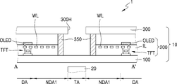
도 2a 내지 도 2c는 본 발명의 실시예들에 따른 표시 장치를 간략하게 나타낸 단면도이다.
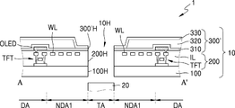
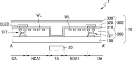
도 3a 내지 도 3c 본 발명의 다른 실시예들에 따른 표시 장치의 단면도이다.
도 4는 본 발명의 일 실시예에 따른 표시 패널을 개략적으로 나타낸 평면도이다.
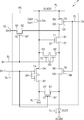
도 5는 본 발명의 일 실시예에 따른 표시 패널 중 어느 한 화소를 나타낸 등가회로도이다.
도 6a는 본 발명의 일 실시예에 따른 표시 패널의 어느 한 화소의 화소회로를 나타낸 평면도이다.
도 6b는 도 6a를 I-I' 선 및 II-II'선으로 자른 단면도에 유기발광소자가 배치된 것을 나타낸 단면도이다.
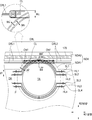
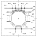
도 7은 본 발명의 일 실시예로서 투과영역 주변의 배선들을 나타낸 평면도이다.
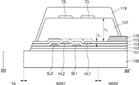
도 8은 도 7을 III-III'선으로 취한 개략적인 단면도이다.
도 9는 본 발명의 실시예와 비교하기 위한 비교예의 개략적인 단면도이다.
도 10은 본 발명의 다른 실시예를 나타낸 평면도이다.
도 11은 본 발명의 또 다른 실시예를 나타낸 개략적인 평면도이다.
도 12는 본 발명의 또 다른 실시예를 나타낸 개략적인 평면도이다.
도 13는 본 발명의 또 다른 실시예를 나타낸 개략적인 평면도이다.
10: 표시 패널
DA: 표시영역
NDA1: 제1비표시영역
NDA2: 제2비표시영역
TA: 투과영역
SL1-SL4: 스캔라인
HL1-HL4: 전극전압라인
DRL:구동배선
CL:연결배선
PL: 구동전압라인
DL: 데이터라인
Claims (20)
- 투과영역, 상기 투과영역을 둘러싸는 제1비표시영역, 및 상기 제1비표시영역을 적어도 일부 둘러싸는 표시영역을 갖는 기판;
상기 표시영역에 배치되며, 화소전극을 갖는 표시요소;
상기 표시영역으로부터 연장되어 상기 제1비표시영역에 배치되며, 상기 투과영역의 가장자리를 따라 우회하는 복수의 스캔라인들;
상기 복수의 스캔라인들과 적어도 일부 중첩되도록 상기 제1비표시영역에 배치되며, 상기 화소전극과 동일층에 배치된 연결배선; 및
상기 연결배선과 다른 층에 배치되어, 콘택홀을 통해 연결된 제1배선 및 제2배선;을 포함하는, 표시 패널. - 제1항에 있어서,
상기 복수의 스캔라인들은 제1방향으로 연장되되, 상기 제1비표시영역에서 만곡부를 포함하며,
상기 연결배선은 상기 제1방향으로 연장되며, 상기 제1비표시영역에서 직선부를 포함하는, 표시 패널. - 제1항에 있어서,
상기 연결배선은 상면이 평탄한 평탄화층 상부에 배치된, 표시 패널. - 제1항에 있어서,
상기 복수의 스캔라인들과 절연층을 사이에 두고 배치되며, 상기 투과영역의 가장자리를 따라 우회하는 복수의 전극전압라인들;을 더 포함하는, 표시 패널. - 제4항에 있어서,
상기 복수의 스캔라인들과 상기 복수의 전극전압라인들은 비중첩되는, 표시 패널. - 제4항에 있어서,
상기 표시영역에는 구동 게이트전극을 포함하는 구동 박막트랜지스터, 및
상기 구동 박막트랜지스터와 중첩 배치된 스토리지 커패시터가 더 배치되며,
상기 복수의 스캔라인들은 상기 구동 게이트전극과 동일층에 배치되며, 상기 복수의 전극전압라인들은 상기 스토리지 커패시터의 제2스토리지 축전판과 동일층에 배치되는, 표시 패널. - 제1항에 있어서,
상기 표시영역 및 제1비표시영역을 둘러싸는 제2비표시영역에 배치되며, 스캔 신호를 제공하는 제1스캔 회로부 및 제2스캔 회로부;를 더 포함하고,
상기 투과영역은 상기 표시영역에 의해서 부분적으로 둘러싸이며,
상기 제1배선은 상기 제1스캔 회로부와 연결되며 상기 제2비표시영역을 따라 연장되며, 상기 제2배선은 상기 제2스캔 회로부 연결되어 상기 제2비표시영역을 따라 연장되는, 표시 패널. - 제7항에 있어서,
상기 제2비표시영역에는 상기 표시영역을 적어도 일부 둘러싸도록 배치되며, 표시영역에 공통전압을 전달하는 공통전원전압배선;이 더 배치되며,
상기 연결배선은 상기 투과영역 및 상기 공통전원전압배선 사이에 배치된, 표시 패널. - 제7항에 있어서,
상기 연결배선과 동일층에 배치되며, 상기 제1비표시영역에서 열린 고리 형상으로 배치된 전극층;을 더 포함하는, 표시 패널. - 제1항에 있어서,
상기 제1비표시영역은 상기 표시영역에 의해서 전체적으로 둘러싸이며,
상기 제1배선 및 상기 제2배선은 상기 표시영역으로부터 연장된, 표시 패널. - 제10항에 있어서,
상기 연결배선은 제1방향으로 연장되며,
상기 제1배선 및 상기 제2배선은 상기 제1방향과 교차되는 제2방향으로 연장된, 표시 패널. - 투과영역, 상기 투과영역을 부분적으로 둘러싸는 표시영역, 및 상기 표시영역 외곽의 비표시영역을 갖는 기판;
상기 표시영역에 배치되며, 화소전극을 갖는 표시요소;
상기 비표시영역에 배치되며, 상기 표시영역을 사이에 두고 배치된 제1스캔 구동회로부 및 제2스캔 구동회로부;
상기 제1스캔 구동회로부에서 연장된 제1구동배선 및 상기 제2스캔 구동회로부에서 연장된 제2구동배선;
상기 제1구동배선 및 상기 제2구동배선을 콘택홀을 통해 연결하는 것으로 상기 화소전극과 동일층에 배치된, 연결배선;을 포함하며,
상기 구동연결선은 상기 투과영역 일측의 비표시영역에 배치된, 표시패널. - 제12항에 있어서,
상기 복수의 스캔라인들은 제1방향으로 연장되되, 상기 제1비표시영역에서 만곡부를 포함하며,
상기 연결배선은 상기 제1방향으로 연장되며, 상기 제1비표시영역에서 직선부를 포함하는, 표시 패널. - 제12항에 있어서,
상기 연결배선은 상면이 평탄한 평탄화층 상부에 배치된, 표시 패널. - 제12항에 있어서,
상기 복수의 스캔라인들과 절연층을 사이에 두고 배치되며, 상기 투과영역의 가장자리를 따라 우회하는 복수의 전극전압라인들;을 더 포함하는, 표시 패널. - 제15항에 있어서,
상기 복수의 전극전압라인들을 덮는 층간절연층;
상기 층간절연층 상에 배치된 데이터라인; 및
상기 데이터라인을 덮는 평탄화층;을 더 포함하며,
상기 제1구동배선 및 상기 제2구동배선은 상기 층간절연층 상에 배치되고,
상기 연결배선은 상기 평탄화층에 배치되며,
상기 평탄화층의 두께는 상기 층간절연층의 두께보다 큰, 표시 패널. - 제15항에 있어서,
상기 표시영역에는 구동 게이트전극을 포함하는 구동 박막트랜지스터, 및
상기 구동 박막트랜지스터와 중첩 배치된 스토리지 커패시터가 더 배치되며,
상기 복수의 스캔라인들은 상기 구동 게이트전극과 동일층에 배치되며, 상기 복수의 전극전압라인들은 상기 스토리지 커패시터의 제2스토리지 축전판과 동일층에 배치되는, 표시 패널. - 제15항에 있어서,
상기 복수의 스캔라인들과 상기 복수의 전극전압라인들은 비중첩되는, 표시 패널. - 제12항에 있어서,
상기 비표시영역에는 상기 표시영역을 적어도 일부 둘러싸도록 배치되며, 표시영역에 공통전압을 전달하는 공통전원전압배선;이 더 배치되며,
상기 연결배선은 상기 투과영역 및 상기 공통전원전압배선 사이에 배치된, 표시 패널. - 제12항에 있어서,
상기 연결배선과 동일층에 배치되며, 상기 제1비표시영역에서 열린 고리 형상으로 배치된 전극층;을 더 포함하는, 표시 패널.
Priority Applications (4)
| Application Number | Priority Date | Filing Date | Title |
|---|---|---|---|
| KR1020180114370A KR102631254B1 (ko) | 2018-09-21 | 2018-09-21 | 표시 패널 |
| US16/382,308 US10847599B2 (en) | 2018-09-21 | 2019-04-12 | Display panel |
| CN201910752019.4A CN110942752B (zh) | 2018-09-21 | 2019-08-15 | 显示面板 |
| US17/079,716 US11653535B2 (en) | 2018-09-21 | 2020-10-26 | Display panel |
Applications Claiming Priority (1)
| Application Number | Priority Date | Filing Date | Title |
|---|---|---|---|
| KR1020180114370A KR102631254B1 (ko) | 2018-09-21 | 2018-09-21 | 표시 패널 |
Publications (2)
| Publication Number | Publication Date |
|---|---|
| KR20200034902A true KR20200034902A (ko) | 2020-04-01 |
| KR102631254B1 KR102631254B1 (ko) | 2024-01-31 |
Family
ID=69883693
Family Applications (1)
| Application Number | Title | Priority Date | Filing Date |
|---|---|---|---|
| KR1020180114370A Active KR102631254B1 (ko) | 2018-09-21 | 2018-09-21 | 표시 패널 |
Country Status (3)
| Country | Link |
|---|---|
| US (2) | US10847599B2 (ko) |
| KR (1) | KR102631254B1 (ko) |
| CN (1) | CN110942752B (ko) |
Cited By (6)
| Publication number | Priority date | Publication date | Assignee | Title |
|---|---|---|---|---|
| KR20210124596A (ko) * | 2020-04-06 | 2021-10-15 | 삼성디스플레이 주식회사 | 표시 패널 및 이를 구비하는 표시 장치 |
| KR20220073316A (ko) * | 2020-11-26 | 2022-06-03 | 엘지디스플레이 주식회사 | 표시장치 |
| KR20220095029A (ko) * | 2020-12-29 | 2022-07-06 | 엘지디스플레이 주식회사 | 표시 장치 |
| US11436976B2 (en) | 2020-07-17 | 2022-09-06 | Samsung Display Co., Ltd. | Display device |
| US12490609B2 (en) | 2023-02-22 | 2025-12-02 | Lg Display Co., Ltd. | Display device comprising an optical area without a signal line |
| US12588359B2 (en) | 2022-02-09 | 2026-03-24 | Samsung Display Co., Ltd. | Display panel and electronic apparatus including the same |
Families Citing this family (32)
| Publication number | Priority date | Publication date | Assignee | Title |
|---|---|---|---|---|
| KR102757333B1 (ko) * | 2018-11-02 | 2025-01-21 | 삼성디스플레이 주식회사 | 표시 패널 |
| KR102517734B1 (ko) * | 2018-12-17 | 2023-04-03 | 엘지디스플레이 주식회사 | 센서패키지 모듈을 포함하는 유기발광 표시장치 |
| JP2020181190A (ja) | 2019-04-24 | 2020-11-05 | 三星ディスプレイ株式會社Samsung Display Co.,Ltd. | 表示装置及びその製造方法 |
| CN110556404A (zh) * | 2019-08-09 | 2019-12-10 | 武汉华星光电半导体显示技术有限公司 | 显示面板及其制备方法、显示装置 |
| CN211044994U (zh) * | 2019-12-10 | 2020-07-17 | 京东方科技集团股份有限公司 | 像素驱动电路、显示面板 |
| CN113013198B (zh) * | 2019-12-20 | 2024-07-16 | 乐金显示有限公司 | 包括用于摄像头的透视区域的显示装置 |
| KR102858762B1 (ko) | 2019-12-20 | 2025-09-10 | 엘지디스플레이 주식회사 | 카메라 투과부를 포함하는 표시 장치 |
| KR20210083795A (ko) | 2019-12-27 | 2021-07-07 | 엘지디스플레이 주식회사 | 표시장치 |
| KR102838512B1 (ko) * | 2020-02-14 | 2025-07-28 | 삼성디스플레이 주식회사 | 표시 장치 |
| CN115136316A (zh) | 2020-02-18 | 2022-09-30 | 谷歌有限责任公司 | 减小显示器中的孔边框区域 |
| KR102932274B1 (ko) * | 2020-02-21 | 2026-02-27 | 삼성디스플레이 주식회사 | 표시 장치 및 표시 장치의 제조방법 |
| CN111402716B (zh) * | 2020-03-27 | 2022-02-18 | 昆山国显光电有限公司 | 阵列基板、显示面板和显示装置 |
| WO2021203329A1 (zh) * | 2020-04-08 | 2021-10-14 | 京东方科技集团股份有限公司 | 显示基板及其制备方法、显示装置 |
| CN113594204B (zh) * | 2020-04-30 | 2024-04-02 | 京东方科技集团股份有限公司 | 显示基板及其制备方法、显示装置 |
| WO2021226785A1 (zh) | 2020-05-11 | 2021-11-18 | 京东方科技集团股份有限公司 | 显示面板和显示装置 |
| KR102767079B1 (ko) * | 2020-05-28 | 2025-02-14 | 삼성디스플레이 주식회사 | 디스플레이 장치 |
| CN111613658B (zh) * | 2020-06-02 | 2023-07-14 | 京东方科技集团股份有限公司 | 显示基板和显示装置 |
| CN113838382B (zh) | 2020-06-05 | 2023-01-31 | 京东方科技集团股份有限公司 | 显示基板以及显示装置 |
| CN113838383B (zh) | 2020-06-05 | 2023-02-03 | 京东方科技集团股份有限公司 | 显示基板以及显示装置 |
| KR102820224B1 (ko) * | 2020-07-08 | 2025-06-16 | 삼성디스플레이 주식회사 | 표시 장치 |
| KR102870765B1 (ko) * | 2020-07-31 | 2025-10-16 | 삼성디스플레이 주식회사 | 전자 장치 |
| WO2022027178A1 (zh) * | 2020-08-03 | 2022-02-10 | 京东方科技集团股份有限公司 | 显示基板和显示装置 |
| KR102883540B1 (ko) * | 2020-09-15 | 2025-11-10 | 삼성디스플레이 주식회사 | 표시 장치 |
| CN120569022A (zh) * | 2020-10-23 | 2025-08-29 | 武汉天马微电子有限公司 | 一种显示面板及显示装置 |
| WO2022133666A1 (zh) * | 2020-12-21 | 2022-06-30 | 京东方科技集团股份有限公司 | 显示面板及其制备方法、显示装置 |
| KR102851615B1 (ko) * | 2020-12-31 | 2025-08-27 | 엘지디스플레이 주식회사 | 폴더블 표시 장치 |
| US12262608B2 (en) * | 2021-06-23 | 2025-03-25 | Chengdu Boe Optoelectronics Technology Co., Ltd. | Display substrate having bezel region at periphery of first display region and second display region and preparation method thereof, and display apparatus having the same |
| KR102884833B1 (ko) * | 2021-09-07 | 2025-11-11 | 엘지디스플레이 주식회사 | 표시 장치 및 그 동작 방법 |
| KR20230103186A (ko) * | 2021-12-31 | 2023-07-07 | 엘지디스플레이 주식회사 | 표시 장치 |
| CN115691325B (zh) * | 2022-09-06 | 2025-07-15 | 武汉天马微电子有限公司 | 显示面板和显示装置 |
| KR20240050530A (ko) * | 2022-10-11 | 2024-04-19 | 삼성디스플레이 주식회사 | 디스플레이 장치 |
| CN116935754B (zh) * | 2023-07-21 | 2026-02-06 | 武汉天马微电子有限公司 | 一种显示面板以及穿戴设备 |
Citations (4)
| Publication number | Priority date | Publication date | Assignee | Title |
|---|---|---|---|---|
| KR20030094656A (ko) * | 2002-06-07 | 2003-12-18 | 엘지전자 주식회사 | 액티브 매트릭스 유기 전계 발광 소자 |
| KR20120080913A (ko) * | 2011-01-10 | 2012-07-18 | 삼성모바일디스플레이주식회사 | 유기 발광 표시 장치 |
| KR20170015632A (ko) * | 2015-07-29 | 2017-02-09 | 엘지디스플레이 주식회사 | 유기발광 다이오드 표시장치 |
| KR20170066767A (ko) * | 2015-12-04 | 2017-06-15 | 삼성디스플레이 주식회사 | 표시 장치 |
Family Cites Families (15)
| Publication number | Priority date | Publication date | Assignee | Title |
|---|---|---|---|---|
| JP2003066488A (ja) * | 2001-08-30 | 2003-03-05 | Hitachi Ltd | 液晶表示装置 |
| US7830591B2 (en) * | 2006-11-20 | 2010-11-09 | Seiko Epson Corporation | Active-matrix circuit board and display |
| KR101440105B1 (ko) * | 2007-02-23 | 2014-09-17 | 삼성전자주식회사 | 멀티 디스플레이 장치 |
| US20080225216A1 (en) * | 2007-03-15 | 2008-09-18 | Seiko Epson Corporation | Active matrix circuit substrate and display device |
| TWI363912B (en) * | 2007-06-20 | 2012-05-11 | Au Optronics Corp | Display panel and fabricating method thereof, electro-optical device comprising said display panel, and fabricating method thereof |
| JP2010032760A (ja) | 2008-07-29 | 2010-02-12 | Hitachi Displays Ltd | 表示装置 |
| KR101127582B1 (ko) | 2010-01-04 | 2012-03-27 | 삼성모바일디스플레이주식회사 | 화소 회로, 유기 전계 발광 표시 장치 및 그 구동 방법 |
| TWI490829B (zh) * | 2013-01-11 | 2015-07-01 | 友達光電股份有限公司 | 顯示面板與顯示裝置 |
| CN103278974B (zh) * | 2013-05-24 | 2016-03-16 | 深圳市华星光电技术有限公司 | 像素单元和阵列基板 |
| KR20170111827A (ko) * | 2016-03-29 | 2017-10-12 | 삼성전자주식회사 | 디스플레이 및 카메라를 포함하는 전자 장치 |
| KR102526110B1 (ko) * | 2016-04-12 | 2023-04-27 | 삼성디스플레이 주식회사 | 표시 장치 및 표시 장치의 제조 방법 |
| US10354578B2 (en) * | 2016-04-15 | 2019-07-16 | Samsung Display Co., Ltd. | Display device |
| CN207216591U (zh) * | 2017-09-20 | 2018-04-10 | 昆山国显光电有限公司 | 触控屏及触控显示装置 |
| CN108183110B (zh) * | 2018-01-12 | 2020-04-14 | 京东方科技集团股份有限公司 | 显示面板和显示装置 |
| US11201307B2 (en) * | 2018-04-17 | 2021-12-14 | Samsung Display Co., Ltd. | Display panel and electronic apparatus including the same |
-
2018
- 2018-09-21 KR KR1020180114370A patent/KR102631254B1/ko active Active
-
2019
- 2019-04-12 US US16/382,308 patent/US10847599B2/en active Active
- 2019-08-15 CN CN201910752019.4A patent/CN110942752B/zh active Active
-
2020
- 2020-10-26 US US17/079,716 patent/US11653535B2/en active Active
Patent Citations (4)
| Publication number | Priority date | Publication date | Assignee | Title |
|---|---|---|---|---|
| KR20030094656A (ko) * | 2002-06-07 | 2003-12-18 | 엘지전자 주식회사 | 액티브 매트릭스 유기 전계 발광 소자 |
| KR20120080913A (ko) * | 2011-01-10 | 2012-07-18 | 삼성모바일디스플레이주식회사 | 유기 발광 표시 장치 |
| KR20170015632A (ko) * | 2015-07-29 | 2017-02-09 | 엘지디스플레이 주식회사 | 유기발광 다이오드 표시장치 |
| KR20170066767A (ko) * | 2015-12-04 | 2017-06-15 | 삼성디스플레이 주식회사 | 표시 장치 |
Cited By (11)
| Publication number | Priority date | Publication date | Assignee | Title |
|---|---|---|---|---|
| KR20210124596A (ko) * | 2020-04-06 | 2021-10-15 | 삼성디스플레이 주식회사 | 표시 패널 및 이를 구비하는 표시 장치 |
| US12610706B2 (en) | 2020-04-06 | 2026-04-21 | Samsung Display Co., Ltd. | Display panel and display apparatus including the same |
| US11436976B2 (en) | 2020-07-17 | 2022-09-06 | Samsung Display Co., Ltd. | Display device |
| US11640789B2 (en) | 2020-07-17 | 2023-05-02 | Samsung Display Co., Ltd. | Display device |
| US12142206B2 (en) | 2020-07-17 | 2024-11-12 | Samsung Display Co., Ltd. | Display device |
| KR20220073316A (ko) * | 2020-11-26 | 2022-06-03 | 엘지디스플레이 주식회사 | 표시장치 |
| US12302736B2 (en) | 2020-11-26 | 2025-05-13 | Lg Display Co., Ltd. | Display apparatus |
| KR20220095029A (ko) * | 2020-12-29 | 2022-07-06 | 엘지디스플레이 주식회사 | 표시 장치 |
| KR20250133620A (ko) * | 2020-12-29 | 2025-09-08 | 엘지디스플레이 주식회사 | 표시 장치 |
| US12588359B2 (en) | 2022-02-09 | 2026-03-24 | Samsung Display Co., Ltd. | Display panel and electronic apparatus including the same |
| US12490609B2 (en) | 2023-02-22 | 2025-12-02 | Lg Display Co., Ltd. | Display device comprising an optical area without a signal line |
Also Published As
| Publication number | Publication date |
|---|---|
| US20200098843A1 (en) | 2020-03-26 |
| KR102631254B1 (ko) | 2024-01-31 |
| CN110942752B (zh) | 2024-02-06 |
| US20210043716A1 (en) | 2021-02-11 |
| US11653535B2 (en) | 2023-05-16 |
| CN110942752A (zh) | 2020-03-31 |
| US10847599B2 (en) | 2020-11-24 |
Similar Documents
| Publication | Publication Date | Title |
|---|---|---|
| KR102631254B1 (ko) | 표시 패널 | |
| KR102516058B1 (ko) | 표시 패널 | |
| KR102851581B1 (ko) | 표시 패널 | |
| KR102881029B1 (ko) | 표시 패널 | |
| KR102770831B1 (ko) | 표시 장치 | |
| KR102739740B1 (ko) | 디스플레이 패널 및 이를 포함한 디스플레이 장치 | |
| EP3739628A1 (en) | Display device | |
| KR20200066505A (ko) | 표시 패널 | |
| KR20200108146A (ko) | 디스플레이 패널 및 이를 포함한 디스플레이 장치 | |
| KR20210059091A (ko) | 표시 장치 | |
| KR20210078650A (ko) | 디스플레이 패널 및 이를 포함하는 디스플레이 장치 | |
| KR20210130902A (ko) | 디스플레이 장치 | |
| KR102935580B1 (ko) | 디스플레이 장치 | |
| CN112447809A (zh) | 显示装置 | |
| KR20210032598A (ko) | 표시 패널 | |
| US20250063911A1 (en) | Display apparatus | |
| CN115955864A (zh) | 显示设备 | |
| KR102869842B1 (ko) | 표시 패널 | |
| US12082459B2 (en) | Display apparatus with connection lines having different curvatures bypassing transmission area | |
| KR102886841B1 (ko) | 표시 장치 | |
| KR20210103632A (ko) | 표시 장치 | |
| CN113053946A (zh) | 显示装置 | |
| KR102960442B1 (ko) | 표시 장치 | |
| KR20210080686A (ko) | 표시 장치 |
Legal Events
| Date | Code | Title | Description |
|---|---|---|---|
| PA0109 | Patent application |
Patent event code: PA01091R01D Comment text: Patent Application Patent event date: 20180921 |
|
| PG1501 | Laying open of application | ||
| A201 | Request for examination | ||
| PA0201 | Request for examination |
Patent event code: PA02012R01D Patent event date: 20210913 Comment text: Request for Examination of Application Patent event code: PA02011R01I Patent event date: 20180921 Comment text: Patent Application |
|
| E902 | Notification of reason for refusal | ||
| PE0902 | Notice of grounds for rejection |
Comment text: Notification of reason for refusal Patent event date: 20221125 Patent event code: PE09021S01D |
|
| E902 | Notification of reason for refusal | ||
| PE0902 | Notice of grounds for rejection |
Comment text: Notification of reason for refusal Patent event date: 20230508 Patent event code: PE09021S01D |
|
| E701 | Decision to grant or registration of patent right | ||
| PE0701 | Decision of registration |
Patent event code: PE07011S01D Comment text: Decision to Grant Registration Patent event date: 20231026 |
|
| GRNT | Written decision to grant | ||
| PR0701 | Registration of establishment |
Comment text: Registration of Establishment Patent event date: 20240125 Patent event code: PR07011E01D |
|
| PR1002 | Payment of registration fee |
Payment date: 20240126 End annual number: 3 Start annual number: 1 |
|
| PG1601 | Publication of registration |