KR20200035320A - 투명 또는 반투명 웨이퍼 상에서의 결함 검출 - Google Patents
투명 또는 반투명 웨이퍼 상에서의 결함 검출 Download PDFInfo
- Publication number
- KR20200035320A KR20200035320A KR1020207008264A KR20207008264A KR20200035320A KR 20200035320 A KR20200035320 A KR 20200035320A KR 1020207008264 A KR1020207008264 A KR 1020207008264A KR 20207008264 A KR20207008264 A KR 20207008264A KR 20200035320 A KR20200035320 A KR 20200035320A
- Authority
- KR
- South Korea
- Prior art keywords
- image
- calculated value
- difference
- controller
- pixel
- Prior art date
- Legal status (The legal status is an assumption and is not a legal conclusion. Google has not performed a legal analysis and makes no representation as to the accuracy of the status listed.)
- Granted
Links
Images


Classifications
-
- H01L22/00—
-
- H—ELECTRICITY
- H10—SEMICONDUCTOR DEVICES; ELECTRIC SOLID-STATE DEVICES NOT OTHERWISE PROVIDED FOR
- H10P—GENERIC PROCESSES OR APPARATUS FOR THE MANUFACTURE OR TREATMENT OF DEVICES COVERED BY CLASS H10
- H10P74/00—Testing or measuring during manufacture or treatment of wafers, substrates or devices
- H10P74/20—Testing or measuring during manufacture or treatment of wafers, substrates or devices characterised by the properties tested or measured, e.g. structural or electrical properties
- H10P74/203—Structural properties, e.g. testing or measuring thicknesses, line widths, warpage, bond strengths or physical defects
-
- G—PHYSICS
- G06—COMPUTING OR CALCULATING; COUNTING
- G06T—IMAGE DATA PROCESSING OR GENERATION, IN GENERAL
- G06T7/00—Image analysis
- G06T7/0002—Inspection of images, e.g. flaw detection
- G06T7/0004—Industrial image inspection
-
- G—PHYSICS
- G01—MEASURING; TESTING
- G01N—INVESTIGATING OR ANALYSING MATERIALS BY DETERMINING THEIR CHEMICAL OR PHYSICAL PROPERTIES
- G01N21/00—Investigating or analysing materials by the use of optical means, i.e. using sub-millimetre waves, infrared, visible or ultraviolet light
- G01N21/84—Systems specially adapted for particular applications
- G01N21/88—Investigating the presence of flaws or contamination
- G01N21/8851—Scan or image signal processing specially adapted therefor, e.g. for scan signal adjustment, for detecting different kinds of defects, for compensating for structures, markings, edges
-
- G—PHYSICS
- G01—MEASURING; TESTING
- G01N—INVESTIGATING OR ANALYSING MATERIALS BY DETERMINING THEIR CHEMICAL OR PHYSICAL PROPERTIES
- G01N21/00—Investigating or analysing materials by the use of optical means, i.e. using sub-millimetre waves, infrared, visible or ultraviolet light
- G01N21/84—Systems specially adapted for particular applications
- G01N21/88—Investigating the presence of flaws or contamination
- G01N21/95—Investigating the presence of flaws or contamination characterised by the material or shape of the object to be examined
- G01N21/958—Inspecting transparent materials or objects, e.g. windscreens
-
- G—PHYSICS
- G03—PHOTOGRAPHY; CINEMATOGRAPHY; ANALOGOUS TECHNIQUES USING WAVES OTHER THAN OPTICAL WAVES; ELECTROGRAPHY; HOLOGRAPHY
- G03F—PHOTOMECHANICAL PRODUCTION OF TEXTURED OR PATTERNED SURFACES, e.g. FOR PRINTING, FOR PROCESSING OF SEMICONDUCTOR DEVICES; MATERIALS THEREFOR; ORIGINALS THEREFOR; APPARATUS SPECIALLY ADAPTED THEREFOR
- G03F7/00—Photomechanical, e.g. photolithographic, production of textured or patterned surfaces, e.g. printing surfaces; Materials therefor, e.g. comprising photoresists; Apparatus specially adapted therefor
- G03F7/70—Microphotolithographic exposure; Apparatus therefor
- G03F7/70483—Information management; Active and passive control; Testing; Wafer monitoring, e.g. pattern monitoring
- G03F7/70605—Workpiece metrology
- G03F7/70616—Monitoring the printed patterns
- G03F7/7065—Defects, e.g. optical inspection of patterned layer for defects
-
- G—PHYSICS
- G03—PHOTOGRAPHY; CINEMATOGRAPHY; ANALOGOUS TECHNIQUES USING WAVES OTHER THAN OPTICAL WAVES; ELECTROGRAPHY; HOLOGRAPHY
- G03F—PHOTOMECHANICAL PRODUCTION OF TEXTURED OR PATTERNED SURFACES, e.g. FOR PRINTING, FOR PROCESSING OF SEMICONDUCTOR DEVICES; MATERIALS THEREFOR; ORIGINALS THEREFOR; APPARATUS SPECIALLY ADAPTED THEREFOR
- G03F7/00—Photomechanical, e.g. photolithographic, production of textured or patterned surfaces, e.g. printing surfaces; Materials therefor, e.g. comprising photoresists; Apparatus specially adapted therefor
- G03F7/70—Microphotolithographic exposure; Apparatus therefor
- G03F7/70483—Information management; Active and passive control; Testing; Wafer monitoring, e.g. pattern monitoring
- G03F7/70605—Workpiece metrology
- G03F7/706835—Metrology information management or control
- G03F7/706837—Data analysis, e.g. filtering, weighting, flyer removal, fingerprints or root cause analysis
-
- G—PHYSICS
- G03—PHOTOGRAPHY; CINEMATOGRAPHY; ANALOGOUS TECHNIQUES USING WAVES OTHER THAN OPTICAL WAVES; ELECTROGRAPHY; HOLOGRAPHY
- G03F—PHOTOMECHANICAL PRODUCTION OF TEXTURED OR PATTERNED SURFACES, e.g. FOR PRINTING, FOR PROCESSING OF SEMICONDUCTOR DEVICES; MATERIALS THEREFOR; ORIGINALS THEREFOR; APPARATUS SPECIALLY ADAPTED THEREFOR
- G03F7/00—Photomechanical, e.g. photolithographic, production of textured or patterned surfaces, e.g. printing surfaces; Materials therefor, e.g. comprising photoresists; Apparatus specially adapted therefor
- G03F7/70—Microphotolithographic exposure; Apparatus therefor
- G03F7/70483—Information management; Active and passive control; Testing; Wafer monitoring, e.g. pattern monitoring
- G03F7/70605—Workpiece metrology
- G03F7/706843—Metrology apparatus
- G03F7/706851—Detection branch, e.g. detector arrangements, polarisation control, wavelength control or dark/bright field detection
-
- G—PHYSICS
- G06—COMPUTING OR CALCULATING; COUNTING
- G06T—IMAGE DATA PROCESSING OR GENERATION, IN GENERAL
- G06T5/00—Image enhancement or restoration
- G06T5/50—Image enhancement or restoration using two or more images, e.g. averaging or subtraction
-
- G—PHYSICS
- G06—COMPUTING OR CALCULATING; COUNTING
- G06T—IMAGE DATA PROCESSING OR GENERATION, IN GENERAL
- G06T7/00—Image analysis
- G06T7/0002—Inspection of images, e.g. flaw detection
- G06T7/0004—Industrial image inspection
- G06T7/001—Industrial image inspection using an image reference approach
-
- G—PHYSICS
- G06—COMPUTING OR CALCULATING; COUNTING
- G06T—IMAGE DATA PROCESSING OR GENERATION, IN GENERAL
- G06T7/00—Image analysis
- G06T7/10—Segmentation; Edge detection
- G06T7/136—Segmentation; Edge detection involving thresholding
-
- H01L22/12—
-
- H01L22/30—
-
- H—ELECTRICITY
- H10—SEMICONDUCTOR DEVICES; ELECTRIC SOLID-STATE DEVICES NOT OTHERWISE PROVIDED FOR
- H10P—GENERIC PROCESSES OR APPARATUS FOR THE MANUFACTURE OR TREATMENT OF DEVICES COVERED BY CLASS H10
- H10P72/00—Handling or holding of wafers, substrates or devices during manufacture or treatment thereof
- H10P72/06—Apparatus for monitoring, sorting, marking, testing or measuring
- H10P72/0616—Monitoring of warpages, curvatures, damages, defects or the like
-
- H—ELECTRICITY
- H10—SEMICONDUCTOR DEVICES; ELECTRIC SOLID-STATE DEVICES NOT OTHERWISE PROVIDED FOR
- H10P—GENERIC PROCESSES OR APPARATUS FOR THE MANUFACTURE OR TREATMENT OF DEVICES COVERED BY CLASS H10
- H10P74/00—Testing or measuring during manufacture or treatment of wafers, substrates or devices
- H10P74/27—Structural arrangements therefor
-
- G—PHYSICS
- G06—COMPUTING OR CALCULATING; COUNTING
- G06T—IMAGE DATA PROCESSING OR GENERATION, IN GENERAL
- G06T2207/00—Indexing scheme for image analysis or image enhancement
- G06T2207/10—Image acquisition modality
- G06T2207/10056—Microscopic image
-
- G—PHYSICS
- G06—COMPUTING OR CALCULATING; COUNTING
- G06T—IMAGE DATA PROCESSING OR GENERATION, IN GENERAL
- G06T2207/00—Indexing scheme for image analysis or image enhancement
- G06T2207/10—Image acquisition modality
- G06T2207/10141—Special mode during image acquisition
- G06T2207/10152—Varying illumination
-
- G—PHYSICS
- G06—COMPUTING OR CALCULATING; COUNTING
- G06T—IMAGE DATA PROCESSING OR GENERATION, IN GENERAL
- G06T2207/00—Indexing scheme for image analysis or image enhancement
- G06T2207/20—Special algorithmic details
- G06T2207/20112—Image segmentation details
- G06T2207/20152—Watershed segmentation
-
- G—PHYSICS
- G06—COMPUTING OR CALCULATING; COUNTING
- G06T—IMAGE DATA PROCESSING OR GENERATION, IN GENERAL
- G06T2207/00—Indexing scheme for image analysis or image enhancement
- G06T2207/20—Special algorithmic details
- G06T2207/20212—Image combination
- G06T2207/20221—Image fusion; Image merging
-
- G—PHYSICS
- G06—COMPUTING OR CALCULATING; COUNTING
- G06T—IMAGE DATA PROCESSING OR GENERATION, IN GENERAL
- G06T2207/00—Indexing scheme for image analysis or image enhancement
- G06T2207/20—Special algorithmic details
- G06T2207/20212—Image combination
- G06T2207/20224—Image subtraction
-
- G—PHYSICS
- G06—COMPUTING OR CALCULATING; COUNTING
- G06T—IMAGE DATA PROCESSING OR GENERATION, IN GENERAL
- G06T2207/00—Indexing scheme for image analysis or image enhancement
- G06T2207/30—Subject of image; Context of image processing
- G06T2207/30108—Industrial image inspection
- G06T2207/30148—Semiconductor; IC; Wafer
-
- G—PHYSICS
- G06—COMPUTING OR CALCULATING; COUNTING
- G06T—IMAGE DATA PROCESSING OR GENERATION, IN GENERAL
- G06T7/00—Image analysis
- G06T7/50—Depth or shape recovery
- G06T7/55—Depth or shape recovery from multiple images
Landscapes
- Engineering & Computer Science (AREA)
- Physics & Mathematics (AREA)
- General Physics & Mathematics (AREA)
- Theoretical Computer Science (AREA)
- Computer Vision & Pattern Recognition (AREA)
- Quality & Reliability (AREA)
- Analytical Chemistry (AREA)
- Pathology (AREA)
- Life Sciences & Earth Sciences (AREA)
- Chemical & Material Sciences (AREA)
- Health & Medical Sciences (AREA)
- Biochemistry (AREA)
- General Health & Medical Sciences (AREA)
- Immunology (AREA)
- Signal Processing (AREA)
- Data Mining & Analysis (AREA)
- Investigating Materials By The Use Of Optical Means Adapted For Particular Applications (AREA)
- Testing Or Measuring Of Semiconductors Or The Like (AREA)
- Manufacturing & Machinery (AREA)
- Image Analysis (AREA)
- Image Processing (AREA)
Abstract
Description
도 1은 유리 웨이퍼의 명시야 및 암시야 이미징 둘 모두를 갖는 세 개의 예시적인 다이를 예시한다;
도 2는 도 1의 다이를 사용한 이미지 감산을 예시한다;
도 3은 유리 웨이퍼의 명시야 이미지의 추가적인 이미지 분석을 제공한다;
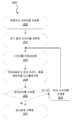
도 4는 본 개시에 따른 방법의 실시형태의 플로우차트이다;
도 5는 단일의 이미지 열에 대한 명시야 이미지를 예시한다;
도 6은 본 개시에 따른 예시적인 명시야 이미지, 예시적인 중앙값 이미지(median image), 및 예시적인 차이 이미지를 예시한다;
도 7은 본 개시에 따른 예시적인 암시야 이미지, 예시적인 중앙값 이미지, 및 예시적인 차이 이미지를 예시한다;
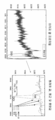
도 8은, 국소적 기준 알고리즘(local reference algorithm; LRA) 및 전통적인 검사 알고리즘의 평가의 파레토(Pareto)를 예시한다;
도 9는 본 개시에 따른 방법의 다른 실시형태의 플로우차트를 예시한다;
도 10은 본 개시에 따른 방법의 여전히 다른 실시형태의 플로우차트를 예시한다;
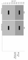
도 11은 본 개시에 따른 시스템의 실시형태의 블록도이다;
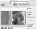
도 12는 본 개시에 따른 원래의 이미지(original image)를 갖는 유저 인터페이스의 실시형태의 이미지이다;
도 13은 본 개시에 따른 필터링된 이미지를 갖는 유저 인터페이스의 실시형태의 이미지이다;
도 14는 본 개시에 따른 차이 이미지를 갖는 유저 인터페이스의 실시형태의 이미지이다;
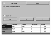
도 15는 본 개시에 따라 레시피를 편집하기 위한 유저 인터페이스의 실시형태의 이미지이다; 그리고
도 16은 LRA에서 사용될 수 있는 결함 속성의 예시적인 테이블이다.
Claims (19)
- 시스템으로서,
프로세서 및 상기 프로세서와 전자 통신하는 전자 데이터 스토리지 유닛을 포함하는 컨트롤러
를 포함하고, 상기 프로세서는 하나 이상의 소프트웨어 모듈을 실행하도록 구성되고, 상기 하나 이상의 소프트웨어 모듈은,
세 개의 다이에 대한 명시야(bright field) 이미지 - 상기 세 개의 다이는 투명 또는 반투명 웨이퍼 상에 있고, 상기 명시야 이미지의 각각은 복수의 이미지 행(row) 및 복수의 이미지 열(column)을 포함함 - 를 수신하고;
상기 세 개의 다이에 대한 암시야(dark field) 이미지 - 상기 암시야 이미지의 각각은 복수의 이미지 행 및 복수의 이미지 열을 포함함 - 를 수신하고;
상기 명시야 이미지 및 상기 암시야 이미지의 상기 이미지 열의 각각에 대한 제1 계산된 값 - 상기 제1 계산된 값은 상기 이미지 열 중 적어도 하나를 따라 적용되는 커널 사이즈(kernel size)에 기초함 - 을 결정하고;
상기 이미지 열의 각각의 픽셀에서의 픽셀 강도로부터 상기 제1 계산된 값을 감산하는 것에 의해 제1 차이를 결정하고;
후보 픽셀 - 상기 후보 픽셀에 대한 상기 제1 차이는 임계치를 초과함 - 을 분류하고;
제2 계산된 값 - 상기 제2 계산된 값은 상기 커널 사이즈에 기초함 - 을 결정하고;
상기 픽셀 강도로부터 상기 제2 계산된 값을 감산하는 것에 의해 제2 차이를 결정하며;
결함을 포함하는 상기 픽셀 - 상기 제2 차이는 결함을 포함하는 상기 픽셀에 대한 상기 임계치를 초과함 - 을 분류하도록 구성된 것인, 시스템. - 제1항에 있어서,
상기 컨트롤러와 전자 통신하는 명시야 이미징 시스템(imaging system)
을 더 포함하는, 시스템. - 제1항에 있어서,
상기 컨트롤러와 전자 통신하는 암시야 이미징 시스템
을 더 포함하는, 시스템. - 제1항에 있어서,
상기 제1 계산된 값은 이동 평균(moving mean)인 것인, 시스템. - 제1항에 있어서,
상기 제2 계산된 값은 국소적 중앙값(local median)인 것인, 시스템. - 제1항에 있어서,
상기 제2 계산된 값은 상기 후보 픽셀의 각각의 것이고, 상기 제2 차이는 상기 후보 픽셀의 각각으로부터 유래된 것인, 시스템. - 제1항에 있어서,
상기 세 개의 다이는 이웃하는 다이인 것인, 시스템. - 방법으로서,
컨트롤러에서, 세 개의 다이에 대한 명시야 이미지 - 상기 세 개의 다이는 투명 또는 반투명 웨이퍼 상에 있고, 상기 명시야 이미지의 각각은 복수의 이미지 행 및 복수의 이미지 열을 포함함 - 를 수신하는 단계;
상기 컨트롤러에서, 상기 세 개의 다이에 대한 암시야 이미지 - 상기 암시야 이미지의 각각은 복수의 이미지 행 및 복수의 이미지 열을 포함함 - 를 수신하는 단계;
상기 컨트롤러를 사용하여, 상기 명시야 이미지 및 상기 암시야 이미지의 상기 이미지 열의 각각에 대한 제1 계산된 값 - 상기 제1 계산된 값은 상기 이미지 열 중 적어도 하나를 따라 적용되는 커널 사이즈에 기초함 - 을 결정하는 단계;
상기 컨트롤러를 사용하여, 상기 이미지 열의 각각의 픽셀에서의 픽셀 강도로부터 상기 제1 계산된 값을 감산하는 것에 의해 제1 차이를 결정하는 단계;
상기 컨트롤러를 사용하여, 후보 픽셀 - 상기 후보 픽셀에 대한 상기 제1 차이는 임계치를 초과함 - 을 분류하는 단계;
상기 컨트롤러를 사용하여, 제2 계산된 값 - 상기 제2 계산된 값은 상기 커널 사이즈에 기초함 - 을 결정하는 단계;
상기 컨트롤러를 사용하여, 상기 픽셀 강도로부터 상기 제2 계산된 값을 감산하는 것에 의해 제2 차이를 결정하는 단계; 및
상기 컨트롤러를 사용하여, 결함을 포함하는 상기 픽셀 - 상기 제2 차이는 결함을 포함하는 상기 픽셀에 대한 상기 임계치를 초과함 - 을 분류하는 단계
를 포함하는, 방법. - 제8항에 있어서,
상기 제1 계산된 값은 이동 평균인 것인, 방법. - 제8항에 있어서,
상기 제2 계산된 값은 국소적 중앙값인 것인, 방법. - 제8항에 있어서,
상기 제1 계산된 값 및 상기 제2 계산된 값 중 하나는 저역 통과 필터를 사용한 고속 푸리에 변환(fast Fourier transform)인 것인, 방법. - 제8항에 있어서,
상기 제1 계산된 값 및 상기 제2 계산된 값 중 하나는 가우시안 커널(Gaussian kernel)과의 컨볼루션인 것인, 방법. - 제8항에 있어서,
상기 제2 계산된 값은 상기 후보 픽셀의 각각의 것이고, 상기 제2 차이는 상기 후보 픽셀의 각각으로부터 유래된 것인, 방법. - 제8항에 있어서,
상기 픽셀 강도는 동일한 다이의 동일한 이미지 열에서의 세 개의 이웃하는 픽셀의 평균이고, 상기 제2 계산된 값은 동일한 다이의 동일한 이미지 열에서의 상기 후보 픽셀 및 두 개의 이웃하는 픽셀의 평균이며, 상기 제2 차이는 상기 후보 픽셀의 상기 평균에 기초한 것인, 방법. - 제8항에 있어서,
상기 제1 계산된 값은 상기 명시야 이미지의 각각 및 상기 암시야 이미지의 각각에 대해 결정된 것인, 방법. - 제8항에 있어서,
상기 제1 계산된 값 및 상기 제2 계산된 값은 상기 명시야 이미지의 각각 및 동일한 다이의 상기 암시야 이미지의 각각 중 대응하는 하나의 융합된 이미지에 기초하여 결정되고, 상기 명시야 이미지의 각각 및 상기 암시야 이미지의 각각 중 상기 대응하는 하나를 융합하여 상기 융합된 이미지를 형성하는 단계
를 더 포함하는, 방법. - 제16항에 있어서,
상기 제2 계산된 값은 국소적 중앙값이고, 상기 제2 계산된 값 및 상기 제2 차이는 상기 명시야 이미지 및 상기 암시야 이미지 둘 모두에 기초하여 결정되며, 상기 임계치는 명시야 임계치 및 암시야 임계치를 포함한 것인, 방법. - 제16항에 있어서,
상기 제2 계산된 값은 국소적 중앙값이고, 상기 임계치는 상기 융합된 이미지에 대한 것이고, 상기 분류하는 단계는, 제1 값 및 제2 값의 곱의 제곱근을 취하여 제3 값을 형성하는 단계 및 상기 제3 값을 상기 임계치에 비교하는 단계를 포함하고, 상기 제1 값은 상기 명시야 이미지의 상기 국소적 중앙값을 뺀 상기 명시야 이미지의 상기 픽셀 강도이고, 상기 제2 값은 상기 암시야 이미지의 상기 국소적 중앙값을 뺀 상기 암시야 이미지의 상기 픽셀 강도인 것인, 방법. - 제8항에 있어서,
상기 세 개의 다이는 이웃하는 다이인 것인, 방법.
Applications Claiming Priority (5)
| Application Number | Priority Date | Filing Date | Title |
|---|---|---|---|
| US201762549775P | 2017-08-24 | 2017-08-24 | |
| US62/549,775 | 2017-08-24 | ||
| US15/803,091 US10402963B2 (en) | 2017-08-24 | 2017-11-03 | Defect detection on transparent or translucent wafers |
| US15/803,091 | 2017-11-03 | ||
| PCT/US2018/047620 WO2019040679A1 (en) | 2017-08-24 | 2018-08-23 | DETECTION OF DEFECTS ON TRANSPARENT OR TRANSLUCENT SLINGS |
Publications (2)
| Publication Number | Publication Date |
|---|---|
| KR20200035320A true KR20200035320A (ko) | 2020-04-02 |
| KR102352701B1 KR102352701B1 (ko) | 2022-01-17 |
Family
ID=65435468
Family Applications (1)
| Application Number | Title | Priority Date | Filing Date |
|---|---|---|---|
| KR1020207008264A Active KR102352701B1 (ko) | 2017-08-24 | 2018-08-23 | 투명 또는 반투명 웨이퍼 상에서의 결함 검출 |
Country Status (7)
| Country | Link |
|---|---|
| US (1) | US10402963B2 (ko) |
| EP (1) | EP3646372B1 (ko) |
| JP (1) | JP7169344B2 (ko) |
| KR (1) | KR102352701B1 (ko) |
| CN (1) | CN111033710B (ko) |
| TW (1) | TWI751372B (ko) |
| WO (1) | WO2019040679A1 (ko) |
Families Citing this family (10)
| Publication number | Priority date | Publication date | Assignee | Title |
|---|---|---|---|---|
| US10402963B2 (en) * | 2017-08-24 | 2019-09-03 | Kla-Tencor Corporation | Defect detection on transparent or translucent wafers |
| CN110363759B (zh) * | 2019-07-22 | 2021-03-19 | 国家超级计算天津中心 | 三维模具调试参数确定方法及装置 |
| US11676260B2 (en) * | 2019-09-26 | 2023-06-13 | Kla Corporation | Variation-based segmentation for wafer defect detection |
| FR3109159B1 (fr) * | 2020-04-09 | 2023-06-23 | Interscience | Procédé de traitement d’images appliqué aux compteurs de colonies en microbiologie |
| JP7418274B2 (ja) * | 2020-04-17 | 2024-01-19 | 東京エレクトロン株式会社 | 異物検査システム、異物検査方法、プログラム及び半導体製造装置 |
| US11631169B2 (en) * | 2020-08-02 | 2023-04-18 | KLA Corp. | Inspection of noisy patterned features |
| US11803960B2 (en) * | 2020-08-12 | 2023-10-31 | Kla Corporation | Optical image contrast metric for optical target search |
| CN115829900A (zh) * | 2021-09-16 | 2023-03-21 | 深圳中科飞测科技股份有限公司 | 检测方法及检测系统、设备和存储介质 |
| CN114937041B (zh) * | 2022-07-25 | 2022-10-25 | 聊城市博源节能科技有限公司 | 一种汽车发动机油路铜套缺陷检测方法及系统 |
| CN116840256B (zh) * | 2023-07-04 | 2026-04-17 | 哈尔滨工业大学 | 一种明暗场融合谐波显微成像装置及方法 |
Citations (3)
| Publication number | Priority date | Publication date | Assignee | Title |
|---|---|---|---|---|
| US702102A (en) * | 1901-06-14 | 1902-06-10 | W A Schrock | Connecting-joint for bedsteads. |
| US5216841A (en) * | 1988-09-16 | 1993-06-08 | Pentti Piilonen | Sharpening device for the blades of a cross-cutting roller |
| US20100183393A1 (en) * | 2007-09-07 | 2010-07-22 | Makino Milling Mahine Co., Ltd. | Method and apparatus for cooling mobile body of machine tool |
Family Cites Families (24)
| Publication number | Priority date | Publication date | Assignee | Title |
|---|---|---|---|---|
| JPH06100555B2 (ja) | 1990-12-19 | 1994-12-12 | 東洋ガラス株式会社 | 透明物体の欠陥検査方法とその装置 |
| JP3148187B2 (ja) * | 1998-10-08 | 2001-03-19 | 日本電気株式会社 | パーティクルモニタシステム及びパーティクル検出方法並びにパーティクル検出プログラムを格納した記録媒体 |
| US6407373B1 (en) * | 1999-06-15 | 2002-06-18 | Applied Materials, Inc. | Apparatus and method for reviewing defects on an object |
| US6809809B2 (en) * | 2000-11-15 | 2004-10-26 | Real Time Metrology, Inc. | Optical method and apparatus for inspecting large area planar objects |
| JP2003149169A (ja) * | 2001-11-16 | 2003-05-21 | Tokyo Seimitsu Co Ltd | ウエハ欠陥検査装置 |
| JP4472341B2 (ja) * | 2001-11-28 | 2010-06-02 | アプライド マテリアルズ インコーポレイテッド | 欠陥検出方法 |
| US6654109B2 (en) * | 2002-02-05 | 2003-11-25 | Taiwan Semiconductor Manufacturing Co. Ltd | System for detecting surface defects in semiconductor wafers |
| TW535207B (en) * | 2002-05-08 | 2003-06-01 | Powerchip Semiconductor Corp | Method for automatically controlling defect-specification in manufacturing process of semiconductors |
| SE526617C2 (sv) | 2003-10-01 | 2005-10-18 | Sick Ivp Ab | System och metod för att avbilda ett objekts egenskaper |
| US7433031B2 (en) * | 2003-10-29 | 2008-10-07 | Core Tech Optical, Inc. | Defect review system with 2D scanning and a ring detector |
| CA2580551A1 (en) | 2004-09-17 | 2006-03-23 | De.Vice Scientific Incorporated | Optical inspection of flat media using direct image technology |
| JP4562126B2 (ja) * | 2004-09-29 | 2010-10-13 | 大日本スクリーン製造株式会社 | 欠陥検出装置および欠陥検出方法 |
| JP4851960B2 (ja) * | 2006-02-24 | 2012-01-11 | 株式会社日立ハイテクノロジーズ | 異物検査方法、および異物検査装置 |
| JP5007979B2 (ja) * | 2008-05-22 | 2012-08-22 | 独立行政法人産業技術総合研究所 | 欠陥を検査する方法及び欠陥検査装置 |
| SG164293A1 (en) | 2009-01-13 | 2010-09-29 | Semiconductor Technologies & Instruments Pte | System and method for inspecting a wafer |
| KR20120093820A (ko) * | 2009-07-01 | 2012-08-23 | 케이엘에이-텐코 코포레이션 | 시변 결함 분류 성능의 모니터링 |
| JPWO2011004534A1 (ja) * | 2009-07-09 | 2012-12-13 | 株式会社日立ハイテクノロジーズ | 半導体欠陥分類方法,半導体欠陥分類装置,半導体欠陥分類プログラム |
| SG177786A1 (en) * | 2010-07-13 | 2012-02-28 | Semiconductor Tech & Instr Inc | System and method for capturing illumination reflected in multiple directions |
| WO2012133591A1 (ja) * | 2011-03-30 | 2012-10-04 | 株式会社 フジミインコーポレーテッド | 研磨用組成物並びにそれを用いた研磨方法及び半導体デバイスの製造方法 |
| JP6080379B2 (ja) * | 2012-04-23 | 2017-02-15 | 株式会社日立ハイテクノロジーズ | 半導体欠陥分類装置及び半導体欠陥分類装置用のプログラム |
| US9189844B2 (en) * | 2012-10-15 | 2015-11-17 | Kla-Tencor Corp. | Detecting defects on a wafer using defect-specific information |
| US9619876B2 (en) | 2013-03-12 | 2017-04-11 | Kla-Tencor Corp. | Detecting defects on wafers based on 2D scatter plots of values determined for output generated using different optics modes |
| CN104008550A (zh) * | 2014-06-05 | 2014-08-27 | 深圳市大族激光科技股份有限公司 | 晶圆表面缺陷特征分析方法、系统、分类方法和系统 |
| US10402963B2 (en) * | 2017-08-24 | 2019-09-03 | Kla-Tencor Corporation | Defect detection on transparent or translucent wafers |
-
2017
- 2017-11-03 US US15/803,091 patent/US10402963B2/en active Active
-
2018
- 2018-08-17 TW TW107128695A patent/TWI751372B/zh active
- 2018-08-23 KR KR1020207008264A patent/KR102352701B1/ko active Active
- 2018-08-23 EP EP18848116.2A patent/EP3646372B1/en active Active
- 2018-08-23 CN CN201880054386.0A patent/CN111033710B/zh active Active
- 2018-08-23 JP JP2020510545A patent/JP7169344B2/ja active Active
- 2018-08-23 WO PCT/US2018/047620 patent/WO2019040679A1/en not_active Ceased
Patent Citations (3)
| Publication number | Priority date | Publication date | Assignee | Title |
|---|---|---|---|---|
| US702102A (en) * | 1901-06-14 | 1902-06-10 | W A Schrock | Connecting-joint for bedsteads. |
| US5216841A (en) * | 1988-09-16 | 1993-06-08 | Pentti Piilonen | Sharpening device for the blades of a cross-cutting roller |
| US20100183393A1 (en) * | 2007-09-07 | 2010-07-22 | Makino Milling Mahine Co., Ltd. | Method and apparatus for cooling mobile body of machine tool |
Also Published As
| Publication number | Publication date |
|---|---|
| WO2019040679A1 (en) | 2019-02-28 |
| US20190066284A1 (en) | 2019-02-28 |
| TWI751372B (zh) | 2022-01-01 |
| CN111033710A (zh) | 2020-04-17 |
| EP3646372A1 (en) | 2020-05-06 |
| US10402963B2 (en) | 2019-09-03 |
| TW201921139A (zh) | 2019-06-01 |
| EP3646372B1 (en) | 2025-10-01 |
| CN111033710B (zh) | 2021-09-24 |
| JP2020532122A (ja) | 2020-11-05 |
| EP3646372A4 (en) | 2021-02-17 |
| KR102352701B1 (ko) | 2022-01-17 |
| JP7169344B2 (ja) | 2022-11-10 |
Similar Documents
| Publication | Publication Date | Title |
|---|---|---|
| KR102352701B1 (ko) | 투명 또는 반투명 웨이퍼 상에서의 결함 검출 | |
| US9916653B2 (en) | Detection of defects embedded in noise for inspection in semiconductor manufacturing | |
| JP5275017B2 (ja) | 欠陥検査方法及びその装置 | |
| CA2638415C (en) | Patterned wafer defect inspection system and method | |
| US10692203B2 (en) | Measuring defectivity by equipping model-less scatterometry with cognitive machine learning | |
| JP4711570B2 (ja) | パターン検査方法及び検査装置 | |
| KR20180117708A (ko) | 제조된 컴포넌트 결함을 국부 적응 문턱값을 사용하여 식별하기 위한 시스템, 방법 및 컴퓨터 프로그램 제품 | |
| KR102440742B1 (ko) | 반도체 소자 검사 시스템 및 그 동작 방법 | |
| US9569834B2 (en) | Automated image-based process monitoring and control | |
| KR20180123173A (ko) | 노이즈 경계 임계값에 의한 웨이퍼 검사 시스템 및 방법 | |
| JP6031151B2 (ja) | 欠陥検査方法及びその装置 | |
| JP5744965B2 (ja) | 欠陥検査方法及びその装置 | |
| EP3289607B1 (en) | Automated image-based process monitoring and control | |
| KR102380099B1 (ko) | 범위 기반 실시간 스캐닝 전자 현미경 비시각적 비너 | |
| KR102719204B1 (ko) | 노이즈 특성에 기초한 서브케어 영역의 클러스터링 | |
| JP2018091771A (ja) | 検査方法、事前画像選別装置及び検査システム | |
| US10372113B2 (en) | Method for defocus detection | |
| JP4827896B2 (ja) | 画像欠陥検査方法、画像欠陥検査装置及び外観検査装置 | |
| KR102589631B1 (ko) | 뉴슨스 맵에 기반한 광대역 플라즈마 검사 | |
| KR20210157792A (ko) | 반도체 소자의 자동화 검사용 레시피 생성을 위한 방법, 컴퓨터 시스템 및 장치 |
Legal Events
| Date | Code | Title | Description |
|---|---|---|---|
| PA0105 | International application |
St.27 status event code: A-0-1-A10-A15-nap-PA0105 |
|
| PG1501 | Laying open of application |
St.27 status event code: A-1-1-Q10-Q12-nap-PG1501 |
|
| A201 | Request for examination | ||
| A302 | Request for accelerated examination | ||
| PA0201 | Request for examination |
St.27 status event code: A-1-2-D10-D11-exm-PA0201 |
|
| PA0302 | Request for accelerated examination |
St.27 status event code: A-1-2-D10-D17-exm-PA0302 St.27 status event code: A-1-2-D10-D16-exm-PA0302 |
|
| E902 | Notification of reason for refusal | ||
| PE0902 | Notice of grounds for rejection |
St.27 status event code: A-1-2-D10-D21-exm-PE0902 |
|
| E13-X000 | Pre-grant limitation requested |
St.27 status event code: A-2-3-E10-E13-lim-X000 |
|
| P11-X000 | Amendment of application requested |
St.27 status event code: A-2-2-P10-P11-nap-X000 |
|
| P13-X000 | Application amended |
St.27 status event code: A-2-2-P10-P13-nap-X000 |
|
| E701 | Decision to grant or registration of patent right | ||
| PE0701 | Decision of registration |
St.27 status event code: A-1-2-D10-D22-exm-PE0701 |
|
| GRNT | Written decision to grant | ||
| PR0701 | Registration of establishment |
St.27 status event code: A-2-4-F10-F11-exm-PR0701 |
|
| PR1002 | Payment of registration fee |
St.27 status event code: A-2-2-U10-U12-oth-PR1002 Fee payment year number: 1 |
|
| PG1601 | Publication of registration |
St.27 status event code: A-4-4-Q10-Q13-nap-PG1601 |
|
| P22-X000 | Classification modified |
St.27 status event code: A-4-4-P10-P22-nap-X000 |
|
| PR1001 | Payment of annual fee |
St.27 status event code: A-4-4-U10-U11-oth-PR1001 Fee payment year number: 4 |
|
| P22-X000 | Classification modified |
St.27 status event code: A-4-4-P10-P22-nap-X000 |