KR20200035797A - 붕소가 도핑된 탄소나노 소재의 제조 방법 - Google Patents
붕소가 도핑된 탄소나노 소재의 제조 방법 Download PDFInfo
- Publication number
- KR20200035797A KR20200035797A KR1020180115373A KR20180115373A KR20200035797A KR 20200035797 A KR20200035797 A KR 20200035797A KR 1020180115373 A KR1020180115373 A KR 1020180115373A KR 20180115373 A KR20180115373 A KR 20180115373A KR 20200035797 A KR20200035797 A KR 20200035797A
- Authority
- KR
- South Korea
- Prior art keywords
- carbon nano
- nano material
- boron
- carbon
- present
- Prior art date
- Legal status (The legal status is an assumption and is not a legal conclusion. Google has not performed a legal analysis and makes no representation as to the accuracy of the status listed.)
- Granted
Links
Images


Classifications
-
- C—CHEMISTRY; METALLURGY
- C01—INORGANIC CHEMISTRY
- C01B—NON-METALLIC ELEMENTS; COMPOUNDS THEREOF; METALLOIDS OR COMPOUNDS THEREOF NOT COVERED BY SUBCLASS C01C
- C01B32/00—Carbon; Compounds thereof
- C01B32/20—Graphite
- C01B32/21—After-treatment
- C01B32/22—Intercalation
-
- C—CHEMISTRY; METALLURGY
- C01—INORGANIC CHEMISTRY
- C01B—NON-METALLIC ELEMENTS; COMPOUNDS THEREOF; METALLOIDS OR COMPOUNDS THEREOF NOT COVERED BY SUBCLASS C01C
- C01B32/00—Carbon; Compounds thereof
- C01B32/15—Nano-sized carbon materials
- C01B32/158—Carbon nanotubes
- C01B32/168—After-treatment
- C01B32/178—Opening; Filling
-
- C—CHEMISTRY; METALLURGY
- C01—INORGANIC CHEMISTRY
- C01P—INDEXING SCHEME RELATING TO STRUCTURAL AND PHYSICAL ASPECTS OF SOLID INORGANIC COMPOUNDS
- C01P2002/00—Crystal-structural characteristics
- C01P2002/50—Solid solutions
- C01P2002/52—Solid solutions containing elements as dopants
- C01P2002/54—Solid solutions containing elements as dopants one element only
Landscapes
- Chemical & Material Sciences (AREA)
- Organic Chemistry (AREA)
- Engineering & Computer Science (AREA)
- Materials Engineering (AREA)
- Nanotechnology (AREA)
- Inorganic Chemistry (AREA)
- Life Sciences & Earth Sciences (AREA)
- General Life Sciences & Earth Sciences (AREA)
- Geology (AREA)
- Carbon And Carbon Compounds (AREA)
Abstract
Description
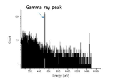
도 2는 본 발명의 일 실시예에 따른 붕소가 도핑된 탄소나노 소재의 제조방법에서, 양성자빔 조사를 통해 생성된 11C 원자의 감마선 에너지를 고순도 게르마늄(HPGe) 검출기로 측정한 것이다.
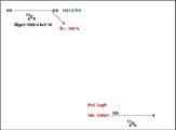
도 3은 본 발명의 일 실시예에 따른 붕소가 도핑된 탄소나노 소재의 제조 방법에서, 11C 동위원소가 11B 원자로 붕괴하면서 도핑되는 방법을 나타낸 것이다.
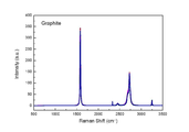
도 4는 본 발명의 일 실시예에 따른 붕소가 도핑된 탄소나노 소재의 제조방법에서, 탄소나노 소재에 붕소의 도핑 전 및 후의 구조적 변형 여부를 라만 분석을 통해 확인한 것이다.
Claims (8)
- 탄소나노 소재에 양성자빔을 조사하여 탄소 원자의 핵반응을 일으키는 단계를 포함하는,
붕소가 도핑된 탄소나노 소재의 제조 방법.
- 제1항에 있어서,
상기 탄소나노 소재는 그라파이트, 탄소나노튜브, 탄소나노점, 그래핀 및 풀러렌으로 이루어진 군에서 선택되는 하나 이상인
붕소가 도핑된 탄소나노 소재의 제조 방법.
- 제1항에 있어서,
상기 핵반응은 12C(p, pn)11C 반응인 것을 특징으로 하는
붕소가 도핑된 탄소나노 소재의 제조 방법.
- 제1항에 있어서,
상기 양성자빔의 에너지는 30 MeV 내지 70 MeV인 것을 특징으로 하는
붕소가 도핑된 탄소나노 소재의 제조 방법.
- 제1항에 있어서,
상기 양성자빔의 조사량은 1x10¹⁵ protons/cm2 내지 1x10¹⁸ protons/cm2인 것을 특징으로 하는
붕소가 도핑된 탄소나노 소재의 제조 방법.
- 제1항에 있어서,
상기 핵반응 단계 후에 생성된 11C 원자가 11B 원자로 붕괴되는 단계를 더 포함하는 것을 특징으로 하는
붕소가 도핑된 탄소나노 소재의 제조 방법.
- 제1항 내지 제6항 중 어느 한 항의 방법으로 제조된 붕소가 도핑된 탄소나노 소재.
- 제7항에 있어서,
상기 붕소가 도핑된 탄소나노 소재는 붕소 원소에 대한 탄소 원소의 함량비(C/B)가 1:1E-6 내지 1:1E-4 인 것을 특징으로 하는
붕소가 도핑된 탄소나노 소재.
Priority Applications (1)
| Application Number | Priority Date | Filing Date | Title |
|---|---|---|---|
| KR1020180115373A KR102142359B1 (ko) | 2018-09-27 | 2018-09-27 | 붕소가 도핑된 탄소나노 소재의 제조 방법 |
Applications Claiming Priority (1)
| Application Number | Priority Date | Filing Date | Title |
|---|---|---|---|
| KR1020180115373A KR102142359B1 (ko) | 2018-09-27 | 2018-09-27 | 붕소가 도핑된 탄소나노 소재의 제조 방법 |
Publications (2)
| Publication Number | Publication Date |
|---|---|
| KR20200035797A true KR20200035797A (ko) | 2020-04-06 |
| KR102142359B1 KR102142359B1 (ko) | 2020-08-07 |
Family
ID=70281908
Family Applications (1)
| Application Number | Title | Priority Date | Filing Date |
|---|---|---|---|
| KR1020180115373A Active KR102142359B1 (ko) | 2018-09-27 | 2018-09-27 | 붕소가 도핑된 탄소나노 소재의 제조 방법 |
Country Status (1)
| Country | Link |
|---|---|
| KR (1) | KR102142359B1 (ko) |
Citations (7)
| Publication number | Priority date | Publication date | Assignee | Title |
|---|---|---|---|---|
| JPH0669494A (ja) * | 1992-08-20 | 1994-03-11 | Hitachi Ltd | カーボン分子とその集合体の製造方法 |
| KR101217209B1 (ko) * | 2010-10-07 | 2012-12-31 | 서울대학교산학협력단 | 발광소자 및 그 제조방법 |
| KR20130076243A (ko) | 2011-12-28 | 2013-07-08 | 재단법인 포항산업과학연구원 | 치환 보론 그래핀 제조방법 |
| JP5561530B2 (ja) * | 2010-03-31 | 2014-07-30 | 古河電気工業株式会社 | 窒化物半導体の炭素ドーピング方法、半導体素子の製造方法 |
| KR20160044618A (ko) * | 2014-10-15 | 2016-04-26 | 한양대학교 산학협력단 | p형 산화물 반도체의 제조방법 및 이 제조방법에 의해 제조되는 p형 산화물 반도체 |
| WO2016133571A2 (en) * | 2014-11-26 | 2016-08-25 | William Marsh Rice University | Laser induced graphene hybrid materials for electronic devices |
| KR101741313B1 (ko) * | 2015-05-14 | 2017-05-30 | 경희대학교 산학협력단 | 이온주입을 통한 지지층 기반의 그래핀의 도핑 방법 |
-
2018
- 2018-09-27 KR KR1020180115373A patent/KR102142359B1/ko active Active
Patent Citations (7)
| Publication number | Priority date | Publication date | Assignee | Title |
|---|---|---|---|---|
| JPH0669494A (ja) * | 1992-08-20 | 1994-03-11 | Hitachi Ltd | カーボン分子とその集合体の製造方法 |
| JP5561530B2 (ja) * | 2010-03-31 | 2014-07-30 | 古河電気工業株式会社 | 窒化物半導体の炭素ドーピング方法、半導体素子の製造方法 |
| KR101217209B1 (ko) * | 2010-10-07 | 2012-12-31 | 서울대학교산학협력단 | 발광소자 및 그 제조방법 |
| KR20130076243A (ko) | 2011-12-28 | 2013-07-08 | 재단법인 포항산업과학연구원 | 치환 보론 그래핀 제조방법 |
| KR20160044618A (ko) * | 2014-10-15 | 2016-04-26 | 한양대학교 산학협력단 | p형 산화물 반도체의 제조방법 및 이 제조방법에 의해 제조되는 p형 산화물 반도체 |
| WO2016133571A2 (en) * | 2014-11-26 | 2016-08-25 | William Marsh Rice University | Laser induced graphene hybrid materials for electronic devices |
| KR101741313B1 (ko) * | 2015-05-14 | 2017-05-30 | 경희대학교 산학협력단 | 이온주입을 통한 지지층 기반의 그래핀의 도핑 방법 |
Non-Patent Citations (1)
| Title |
|---|
| Nanotechnology 17 (2006) 5675-5680 * |
Also Published As
| Publication number | Publication date |
|---|---|
| KR102142359B1 (ko) | 2020-08-07 |
Similar Documents
| Publication | Publication Date | Title |
|---|---|---|
| Shanmugam et al. | A review of the synthesis, properties, and applications of 2D materials | |
| Miyazawa | Synthesis of fullerene nanowhiskers using the liquid–liquid interfacial precipitation method and their mechanical, electrical and superconducting properties | |
| Liu et al. | Development of a Seedless Floating Growth Process in Solution for Synthesis of Crystalline ZnO Micro/Nanowire Arrays on Graphene: Towards High‐Performance Nanohybrid Ultraviolet Photodetectors | |
| Li et al. | Synthesis of wafer-scale ultrathin graphdiyne for flexible optoelectronic memory with over 256 storage levels | |
| Siqueira Jr et al. | Carbon-based nanomaterials | |
| Bellucci | Carbon nanotubes: physics and applications | |
| Chowdhury et al. | Exotic physics and chemistry of two-dimensional phosphorus: phosphorene | |
| Artyukhov et al. | Flexoelectricity and charge separation in carbon nanotubes | |
| McMorrow et al. | Radiation-hard complementary integrated circuits based on semiconducting single-walled carbon nanotubes | |
| Zhang et al. | Enhanced cold field emission of large-area arrays of vertically aligned ZnO-nanotapers via sharpening: experiment and theory | |
| Zhang et al. | CuI Encapsulated within Single‐Walled Carbon Nanotube Networks with High Current Carrying Capacity and Excellent Conductivity | |
| Umeta et al. | C60-nanowire two-state resistance switching based on fullerene polymerization/depolymerization | |
| Yusupov et al. | Enhancing the thermoelectric performance of single-walled carbon nanotube-conducting polymer nanocomposites | |
| Muramatsu et al. | Outer tube-selectively boron-doped double-walled carbon nanotubes for thermoelectric applications | |
| Umeta et al. | Stable Resistance Switching in Lu3N@ C80 Nanowires Promoted by the Endohedral Effect: Implications for Single-Fullerene Motion Resistance Switching | |
| Cao et al. | Fabrication of rare-earth biphthalocyanine encapsulated by carbon nanotubes using a capillary filling method | |
| Ishii et al. | High-conductivity boron-doped carbon nanotubes | |
| Wei et al. | Synthesis and photoelectric properties of coaxial Schottky junctions of ZnS and carbon nanotubes | |
| KR102142359B1 (ko) | 붕소가 도핑된 탄소나노 소재의 제조 방법 | |
| Alegaonkar et al. | Nanocarbons: Preparation, Assessments, and Applications | |
| Semet et al. | Field emission behavior of vertically aligned ZnO nanowire planar cathodes | |
| Kalavakunda et al. | Graphene and its analogues | |
| Omeer et al. | Tuning the band gap in graphene nanoflakes via various impurities | |
| Fan et al. | Controllable synthesis of flake-like Al-doped ZnO nanostructures and its application in inverted organic solar cells | |
| Soler | Fabrication and characterization of macroscopic graphene layers on metallic substrates |
Legal Events
| Date | Code | Title | Description |
|---|---|---|---|
| PA0109 | Patent application |
St.27 status event code: A-0-1-A10-A12-nap-PA0109 |
|
| PA0201 | Request for examination |
St.27 status event code: A-1-2-D10-D11-exm-PA0201 |
|
| D13-X000 | Search requested |
St.27 status event code: A-1-2-D10-D13-srh-X000 |
|
| D14-X000 | Search report completed |
St.27 status event code: A-1-2-D10-D14-srh-X000 |
|
| E902 | Notification of reason for refusal | ||
| PE0902 | Notice of grounds for rejection |
St.27 status event code: A-1-2-D10-D21-exm-PE0902 |
|
| PG1501 | Laying open of application |
St.27 status event code: A-1-1-Q10-Q12-nap-PG1501 |
|
| E13-X000 | Pre-grant limitation requested |
St.27 status event code: A-2-3-E10-E13-lim-X000 |
|
| P11-X000 | Amendment of application requested |
St.27 status event code: A-2-2-P10-P11-nap-X000 |
|
| P13-X000 | Application amended |
St.27 status event code: A-2-2-P10-P13-nap-X000 |
|
| E701 | Decision to grant or registration of patent right | ||
| PE0701 | Decision of registration |
St.27 status event code: A-1-2-D10-D22-exm-PE0701 |
|
| GRNT | Written decision to grant | ||
| PR0701 | Registration of establishment |
St.27 status event code: A-2-4-F10-F11-exm-PR0701 |
|
| PR1002 | Payment of registration fee |
St.27 status event code: A-2-2-U10-U11-oth-PR1002 Fee payment year number: 1 |
|
| PG1601 | Publication of registration |
St.27 status event code: A-4-4-Q10-Q13-nap-PG1601 |
|
| PR1001 | Payment of annual fee |
St.27 status event code: A-4-4-U10-U11-oth-PR1001 Fee payment year number: 4 |
|
| PR1001 | Payment of annual fee |
St.27 status event code: A-4-4-U10-U11-oth-PR1001 Fee payment year number: 5 |
|
| PN2301 | Change of applicant |
St.27 status event code: A-5-5-R10-R13-asn-PN2301 St.27 status event code: A-5-5-R10-R11-asn-PN2301 |
|
| PR1001 | Payment of annual fee |
St.27 status event code: A-4-4-U10-U11-oth-PR1001 Fee payment year number: 6 |
|
| PN2301 | Change of applicant |
St.27 status event code: A-5-5-R10-R11-asn-PN2301 |
|
| R11 | Change to the name of applicant or owner or transfer of ownership requested |
Free format text: ST27 STATUS EVENT CODE: A-5-5-R10-R11-ASN-PN2301 (AS PROVIDED BY THE NATIONAL OFFICE) |
|
| PN2301 | Change of applicant |
St.27 status event code: A-5-5-R10-R14-asn-PN2301 |
|
| R14 | Transfer of ownership recorded |
Free format text: ST27 STATUS EVENT CODE: A-5-5-R10-R14-ASN-PN2301 (AS PROVIDED BY THE NATIONAL OFFICE) |
|
| R18 | Changes to party contact information recorded |
Free format text: ST27 STATUS EVENT CODE: A-5-5-R10-R18-OTH-X000 (AS PROVIDED BY THE NATIONAL OFFICE) |
|
| R18-X000 | Changes to party contact information recorded |
St.27 status event code: A-5-5-R10-R18-oth-X000 |