KR20200035940A - 촬상 소자, 적층형 촬상 소자 및 고체 촬상 장치 - Google Patents
촬상 소자, 적층형 촬상 소자 및 고체 촬상 장치 Download PDFInfo
- Publication number
- KR20200035940A KR20200035940A KR1020207000827A KR20207000827A KR20200035940A KR 20200035940 A KR20200035940 A KR 20200035940A KR 1020207000827 A KR1020207000827 A KR 1020207000827A KR 20207000827 A KR20207000827 A KR 20207000827A KR 20200035940 A KR20200035940 A KR 20200035940A
- Authority
- KR
- South Korea
- Prior art keywords
- electrode
- layer
- photoelectric conversion
- charge accumulation
- composite oxide
- Prior art date
- Legal status (The legal status is an assumption and is not a legal conclusion. Google has not performed a legal analysis and makes no representation as to the accuracy of the status listed.)
- Granted
Links
- 238000003384 imaging method Methods 0.000 title claims abstract description 817
- 238000006243 chemical reaction Methods 0.000 claims abstract description 546
- 239000002131 composite material Substances 0.000 claims abstract description 289
- 229910052738 indium Inorganic materials 0.000 claims abstract description 57
- APFVFJFRJDLVQX-UHFFFAOYSA-N indium atom Chemical compound [In] APFVFJFRJDLVQX-UHFFFAOYSA-N 0.000 claims abstract description 56
- 239000000203 mixture Substances 0.000 claims abstract description 53
- 239000011701 zinc Substances 0.000 claims abstract description 38
- 229910052725 zinc Inorganic materials 0.000 claims abstract description 32
- GYHNNYVSQQEPJS-UHFFFAOYSA-N Gallium Chemical compound [Ga] GYHNNYVSQQEPJS-UHFFFAOYSA-N 0.000 claims abstract description 18
- HCHKCACWOHOZIP-UHFFFAOYSA-N Zinc Chemical compound [Zn] HCHKCACWOHOZIP-UHFFFAOYSA-N 0.000 claims abstract description 18
- 229910052733 gallium Inorganic materials 0.000 claims abstract description 18
- 238000009825 accumulation Methods 0.000 claims description 443
- 238000012546 transfer Methods 0.000 claims description 133
- 238000000034 method Methods 0.000 claims description 93
- 229910005191 Ga 2 O 3 Inorganic materials 0.000 claims description 8
- 239000010410 layer Substances 0.000 description 1125
- 239000004065 semiconductor Substances 0.000 description 122
- 238000003860 storage Methods 0.000 description 78
- 238000007667 floating Methods 0.000 description 77
- 238000009792 diffusion process Methods 0.000 description 75
- 239000000758 substrate Substances 0.000 description 70
- 230000004048 modification Effects 0.000 description 69
- 238000012986 modification Methods 0.000 description 69
- 239000000463 material Substances 0.000 description 49
- 239000010408 film Substances 0.000 description 46
- 230000036961 partial effect Effects 0.000 description 45
- 238000010586 diagram Methods 0.000 description 44
- 239000004020 conductor Substances 0.000 description 33
- 230000005540 biological transmission Effects 0.000 description 31
- XLOMVQKBTHCTTD-UHFFFAOYSA-N Zinc monoxide Chemical compound [Zn]=O XLOMVQKBTHCTTD-UHFFFAOYSA-N 0.000 description 28
- 238000004544 sputter deposition Methods 0.000 description 24
- 239000011229 interlayer Substances 0.000 description 23
- 238000012545 processing Methods 0.000 description 20
- 239000011135 tin Substances 0.000 description 19
- 230000015572 biosynthetic process Effects 0.000 description 17
- 230000035945 sensitivity Effects 0.000 description 17
- 230000006870 function Effects 0.000 description 15
- 239000011787 zinc oxide Substances 0.000 description 15
- -1 C60 Chemical class 0.000 description 14
- XUIMIQQOPSSXEZ-UHFFFAOYSA-N Silicon Chemical compound [Si] XUIMIQQOPSSXEZ-UHFFFAOYSA-N 0.000 description 13
- 229910052710 silicon Inorganic materials 0.000 description 13
- 239000010703 silicon Substances 0.000 description 13
- 230000000875 corresponding effect Effects 0.000 description 12
- 230000003287 optical effect Effects 0.000 description 10
- 125000004430 oxygen atom Chemical group O* 0.000 description 10
- XMWRBQBLMFGWIX-UHFFFAOYSA-N C60 fullerene Chemical class C12=C3C(C4=C56)=C7C8=C5C5=C9C%10=C6C6=C4C1=C1C4=C6C6=C%10C%10=C9C9=C%11C5=C8C5=C8C7=C3C3=C7C2=C1C1=C2C4=C6C4=C%10C6=C9C9=C%11C5=C5C8=C3C3=C7C1=C1C2=C4C6=C2C9=C5C3=C12 XMWRBQBLMFGWIX-UHFFFAOYSA-N 0.000 description 9
- ATJFFYVFTNAWJD-UHFFFAOYSA-N Tin Chemical compound [Sn] ATJFFYVFTNAWJD-UHFFFAOYSA-N 0.000 description 9
- 238000005229 chemical vapour deposition Methods 0.000 description 9
- 238000000151 deposition Methods 0.000 description 9
- 239000011810 insulating material Substances 0.000 description 9
- 229910052718 tin Inorganic materials 0.000 description 9
- 229910052782 aluminium Inorganic materials 0.000 description 8
- XAGFODPZIPBFFR-UHFFFAOYSA-N aluminium Chemical compound [Al] XAGFODPZIPBFFR-UHFFFAOYSA-N 0.000 description 8
- 230000008859 change Effects 0.000 description 8
- 239000010949 copper Substances 0.000 description 8
- 239000011368 organic material Substances 0.000 description 8
- WFKWXMTUELFFGS-UHFFFAOYSA-N tungsten Chemical compound [W] WFKWXMTUELFFGS-UHFFFAOYSA-N 0.000 description 8
- 229910052721 tungsten Inorganic materials 0.000 description 8
- 239000010937 tungsten Substances 0.000 description 8
- KDLHZDBZIXYQEI-UHFFFAOYSA-N Palladium Chemical compound [Pd] KDLHZDBZIXYQEI-UHFFFAOYSA-N 0.000 description 7
- 239000002019 doping agent Substances 0.000 description 7
- 230000005684 electric field Effects 0.000 description 7
- 238000005530 etching Methods 0.000 description 7
- 229910003437 indium oxide Inorganic materials 0.000 description 7
- PJXISJQVUVHSOJ-UHFFFAOYSA-N indium(iii) oxide Chemical compound [O-2].[O-2].[O-2].[In+3].[In+3] PJXISJQVUVHSOJ-UHFFFAOYSA-N 0.000 description 7
- 229910052751 metal Inorganic materials 0.000 description 7
- BASFCYQUMIYNBI-UHFFFAOYSA-N platinum Chemical compound [Pt] BASFCYQUMIYNBI-UHFFFAOYSA-N 0.000 description 7
- 230000008569 process Effects 0.000 description 7
- PXHVJJICTQNCMI-UHFFFAOYSA-N Nickel Chemical compound [Ni] PXHVJJICTQNCMI-UHFFFAOYSA-N 0.000 description 6
- 229910020994 Sn-Zn Inorganic materials 0.000 description 6
- 229910009069 Sn—Zn Inorganic materials 0.000 description 6
- 230000003321 amplification Effects 0.000 description 6
- 230000000903 blocking effect Effects 0.000 description 6
- 239000000969 carrier Substances 0.000 description 6
- 239000011651 chromium Substances 0.000 description 6
- 230000001276 controlling effect Effects 0.000 description 6
- 229910003472 fullerene Inorganic materials 0.000 description 6
- 239000007789 gas Substances 0.000 description 6
- 229910052809 inorganic oxide Inorganic materials 0.000 description 6
- 239000002184 metal Substances 0.000 description 6
- 238000003199 nucleic acid amplification method Methods 0.000 description 6
- 239000000049 pigment Substances 0.000 description 6
- PMJMHCXAGMRGBZ-UHFFFAOYSA-N subphthalocyanine Chemical class N1C(N=C2C3=CC=CC=C3C(=N3)N2)=C(C=CC=C2)C2=C1N=C1C2=CC=CC=C2C3=N1 PMJMHCXAGMRGBZ-UHFFFAOYSA-N 0.000 description 6
- BQCADISMDOOEFD-UHFFFAOYSA-N Silver Chemical compound [Ag] BQCADISMDOOEFD-UHFFFAOYSA-N 0.000 description 5
- 238000005520 cutting process Methods 0.000 description 5
- 239000000975 dye Substances 0.000 description 5
- 150000002222 fluorine compounds Chemical class 0.000 description 5
- 238000010438 heat treatment Methods 0.000 description 5
- QGLKJKCYBOYXKC-UHFFFAOYSA-N nonaoxidotritungsten Chemical compound O=[W]1(=O)O[W](=O)(=O)O[W](=O)(=O)O1 QGLKJKCYBOYXKC-UHFFFAOYSA-N 0.000 description 5
- 229910052709 silver Inorganic materials 0.000 description 5
- 239000004332 silver Substances 0.000 description 5
- 239000010936 titanium Substances 0.000 description 5
- 229910001930 tungsten oxide Inorganic materials 0.000 description 5
- RYGMFSIKBFXOCR-UHFFFAOYSA-N Copper Chemical compound [Cu] RYGMFSIKBFXOCR-UHFFFAOYSA-N 0.000 description 4
- MYMOFIZGZYHOMD-UHFFFAOYSA-N Dioxygen Chemical compound O=O MYMOFIZGZYHOMD-UHFFFAOYSA-N 0.000 description 4
- 230000002411 adverse Effects 0.000 description 4
- 229910045601 alloy Inorganic materials 0.000 description 4
- 239000000956 alloy Substances 0.000 description 4
- 238000004458 analytical method Methods 0.000 description 4
- 229910052802 copper Inorganic materials 0.000 description 4
- 229910001882 dioxygen Inorganic materials 0.000 description 4
- 238000009826 distribution Methods 0.000 description 4
- 238000010894 electron beam technology Methods 0.000 description 4
- 239000010931 gold Substances 0.000 description 4
- 238000007733 ion plating Methods 0.000 description 4
- 238000002955 isolation Methods 0.000 description 4
- 238000001755 magnetron sputter deposition Methods 0.000 description 4
- 150000002739 metals Chemical class 0.000 description 4
- 238000001451 molecular beam epitaxy Methods 0.000 description 4
- 238000005240 physical vapour deposition Methods 0.000 description 4
- 230000002829 reductive effect Effects 0.000 description 4
- 230000002441 reversible effect Effects 0.000 description 4
- 230000003746 surface roughness Effects 0.000 description 4
- 230000008719 thickening Effects 0.000 description 4
- VYZAMTAEIAYCRO-UHFFFAOYSA-N Chromium Chemical compound [Cr] VYZAMTAEIAYCRO-UHFFFAOYSA-N 0.000 description 3
- NRCMAYZCPIVABH-UHFFFAOYSA-N Quinacridone Chemical class N1C2=CC=CC=C2C(=O)C2=C1C=C1C(=O)C3=CC=CC=C3NC1=C2 NRCMAYZCPIVABH-UHFFFAOYSA-N 0.000 description 3
- VYPSYNLAJGMNEJ-UHFFFAOYSA-N Silicium dioxide Chemical compound O=[Si]=O VYPSYNLAJGMNEJ-UHFFFAOYSA-N 0.000 description 3
- 229910006404 SnO 2 Inorganic materials 0.000 description 3
- RTAQQCXQSZGOHL-UHFFFAOYSA-N Titanium Chemical compound [Ti] RTAQQCXQSZGOHL-UHFFFAOYSA-N 0.000 description 3
- YXFVVABEGXRONW-UHFFFAOYSA-N Toluene Chemical compound CC1=CC=CC=C1 YXFVVABEGXRONW-UHFFFAOYSA-N 0.000 description 3
- 239000011575 calcium Substances 0.000 description 3
- 229910052804 chromium Inorganic materials 0.000 description 3
- 150000001875 compounds Chemical class 0.000 description 3
- 229910001195 gallium oxide Inorganic materials 0.000 description 3
- 238000005286 illumination Methods 0.000 description 3
- 238000002347 injection Methods 0.000 description 3
- 239000007924 injection Substances 0.000 description 3
- 238000009413 insulation Methods 0.000 description 3
- 239000011777 magnesium Substances 0.000 description 3
- 238000004519 manufacturing process Methods 0.000 description 3
- DZVCFNFOPIZQKX-LTHRDKTGSA-M merocyanine Chemical compound [Na+].O=C1N(CCCC)C(=O)N(CCCC)C(=O)C1=C\C=C\C=C/1N(CCCS([O-])(=O)=O)C2=CC=CC=C2O\1 DZVCFNFOPIZQKX-LTHRDKTGSA-M 0.000 description 3
- 229910044991 metal oxide Inorganic materials 0.000 description 3
- 150000004706 metal oxides Chemical class 0.000 description 3
- VLKZOEOYAKHREP-UHFFFAOYSA-N n-Hexane Chemical compound CCCCCC VLKZOEOYAKHREP-UHFFFAOYSA-N 0.000 description 3
- 229910052763 palladium Inorganic materials 0.000 description 3
- 239000002245 particle Substances 0.000 description 3
- 229910052697 platinum Inorganic materials 0.000 description 3
- 229920001721 polyimide Polymers 0.000 description 3
- 229920005989 resin Polymers 0.000 description 3
- 239000011347 resin Substances 0.000 description 3
- 230000004044 response Effects 0.000 description 3
- 239000011669 selenium Substances 0.000 description 3
- 229910052814 silicon oxide Inorganic materials 0.000 description 3
- 239000011734 sodium Substances 0.000 description 3
- JBQYATWDVHIOAR-UHFFFAOYSA-N tellanylidenegermanium Chemical compound [Te]=[Ge] JBQYATWDVHIOAR-UHFFFAOYSA-N 0.000 description 3
- 229910052719 titanium Inorganic materials 0.000 description 3
- TYHJXGDMRRJCRY-UHFFFAOYSA-N zinc indium(3+) oxygen(2-) tin(4+) Chemical compound [O-2].[Zn+2].[Sn+4].[In+3] TYHJXGDMRRJCRY-UHFFFAOYSA-N 0.000 description 3
- BCMCBBGGLRIHSE-UHFFFAOYSA-N 1,3-benzoxazole Chemical class C1=CC=C2OC=NC2=C1 BCMCBBGGLRIHSE-UHFFFAOYSA-N 0.000 description 2
- UUEWCQRISZBELL-UHFFFAOYSA-N 3-trimethoxysilylpropane-1-thiol Chemical compound CO[Si](OC)(OC)CCCS UUEWCQRISZBELL-UHFFFAOYSA-N 0.000 description 2
- 229910018072 Al 2 O 3 Inorganic materials 0.000 description 2
- XKRFYHLGVUSROY-UHFFFAOYSA-N Argon Chemical compound [Ar] XKRFYHLGVUSROY-UHFFFAOYSA-N 0.000 description 2
- OKTJSMMVPCPJKN-UHFFFAOYSA-N Carbon Chemical compound [C] OKTJSMMVPCPJKN-UHFFFAOYSA-N 0.000 description 2
- HEDRZPFGACZZDS-UHFFFAOYSA-N Chloroform Chemical compound ClC(Cl)Cl HEDRZPFGACZZDS-UHFFFAOYSA-N 0.000 description 2
- LFQSCWFLJHTTHZ-UHFFFAOYSA-N Ethanol Chemical compound CCO LFQSCWFLJHTTHZ-UHFFFAOYSA-N 0.000 description 2
- YCKRFDGAMUMZLT-UHFFFAOYSA-N Fluorine atom Chemical compound [F] YCKRFDGAMUMZLT-UHFFFAOYSA-N 0.000 description 2
- XEEYBQQBJWHFJM-UHFFFAOYSA-N Iron Chemical compound [Fe] XEEYBQQBJWHFJM-UHFFFAOYSA-N 0.000 description 2
- 229920001609 Poly(3,4-ethylenedioxythiophene) Polymers 0.000 description 2
- 229920001665 Poly-4-vinylphenol Polymers 0.000 description 2
- 239000004642 Polyimide Substances 0.000 description 2
- 239000004372 Polyvinyl alcohol Substances 0.000 description 2
- BUGBHKTXTAQXES-UHFFFAOYSA-N Selenium Chemical compound [Se] BUGBHKTXTAQXES-UHFFFAOYSA-N 0.000 description 2
- 238000002441 X-ray diffraction Methods 0.000 description 2
- BSUHXFDAHXCSQL-UHFFFAOYSA-N [Zn+2].[W+4].[O-2].[In+3] Chemical compound [Zn+2].[W+4].[O-2].[In+3] BSUHXFDAHXCSQL-UHFFFAOYSA-N 0.000 description 2
- 238000010521 absorption reaction Methods 0.000 description 2
- 239000002253 acid Substances 0.000 description 2
- 229910052783 alkali metal Inorganic materials 0.000 description 2
- 150000001340 alkali metals Chemical class 0.000 description 2
- 229910052784 alkaline earth metal Inorganic materials 0.000 description 2
- 150000001342 alkaline earth metals Chemical class 0.000 description 2
- 229910021417 amorphous silicon Inorganic materials 0.000 description 2
- 229910052791 calcium Inorganic materials 0.000 description 2
- 125000000609 carbazolyl group Chemical class C1(=CC=CC=2C3=CC=CC=C3NC12)* 0.000 description 2
- 238000003486 chemical etching Methods 0.000 description 2
- 238000000576 coating method Methods 0.000 description 2
- 239000003086 colorant Substances 0.000 description 2
- 230000000295 complement effect Effects 0.000 description 2
- ZYGHJZDHTFUPRJ-UHFFFAOYSA-N coumarin Chemical compound C1=CC=C2OC(=O)C=CC2=C1 ZYGHJZDHTFUPRJ-UHFFFAOYSA-N 0.000 description 2
- 238000001514 detection method Methods 0.000 description 2
- JAONJTDQXUSBGG-UHFFFAOYSA-N dialuminum;dizinc;oxygen(2-) Chemical compound [O-2].[O-2].[O-2].[O-2].[O-2].[Al+3].[Al+3].[Zn+2].[Zn+2] JAONJTDQXUSBGG-UHFFFAOYSA-N 0.000 description 2
- AJNVQOSZGJRYEI-UHFFFAOYSA-N digallium;oxygen(2-) Chemical compound [O-2].[O-2].[O-2].[Ga+3].[Ga+3] AJNVQOSZGJRYEI-UHFFFAOYSA-N 0.000 description 2
- 239000011737 fluorine Substances 0.000 description 2
- 229910052731 fluorine Inorganic materials 0.000 description 2
- PCHJSUWPFVWCPO-UHFFFAOYSA-N gold Chemical compound [Au] PCHJSUWPFVWCPO-UHFFFAOYSA-N 0.000 description 2
- 229910052737 gold Inorganic materials 0.000 description 2
- 238000007646 gravure printing Methods 0.000 description 2
- 229910052735 hafnium Inorganic materials 0.000 description 2
- 150000002391 heterocyclic compounds Chemical class 0.000 description 2
- 150000002460 imidazoles Chemical class 0.000 description 2
- 230000006872 improvement Effects 0.000 description 2
- AMGQUBHHOARCQH-UHFFFAOYSA-N indium;oxotin Chemical compound [In].[Sn]=O AMGQUBHHOARCQH-UHFFFAOYSA-N 0.000 description 2
- ATFCOADKYSRZES-UHFFFAOYSA-N indium;oxotungsten Chemical compound [In].[W]=O ATFCOADKYSRZES-UHFFFAOYSA-N 0.000 description 2
- 229910010272 inorganic material Inorganic materials 0.000 description 2
- 239000011147 inorganic material Substances 0.000 description 2
- 238000003475 lamination Methods 0.000 description 2
- 238000000608 laser ablation Methods 0.000 description 2
- 229910052744 lithium Inorganic materials 0.000 description 2
- 229910052749 magnesium Inorganic materials 0.000 description 2
- 239000011159 matrix material Substances 0.000 description 2
- 239000012528 membrane Substances 0.000 description 2
- 238000000813 microcontact printing Methods 0.000 description 2
- 229910052759 nickel Inorganic materials 0.000 description 2
- 238000007645 offset printing Methods 0.000 description 2
- 239000012044 organic layer Substances 0.000 description 2
- 125000002524 organometallic group Chemical group 0.000 description 2
- TWNQGVIAIRXVLR-UHFFFAOYSA-N oxo(oxoalumanyloxy)alumane Chemical compound O=[Al]O[Al]=O TWNQGVIAIRXVLR-UHFFFAOYSA-N 0.000 description 2
- KYKLWYKWCAYAJY-UHFFFAOYSA-N oxotin;zinc Chemical compound [Zn].[Sn]=O KYKLWYKWCAYAJY-UHFFFAOYSA-N 0.000 description 2
- 238000000059 patterning Methods 0.000 description 2
- 230000002093 peripheral effect Effects 0.000 description 2
- 125000002080 perylenyl group Chemical group C1(=CC=C2C=CC=C3C4=CC=CC5=CC=CC(C1=C23)=C45)* 0.000 description 2
- 230000005622 photoelectricity Effects 0.000 description 2
- 238000000206 photolithography Methods 0.000 description 2
- IEQIEDJGQAUEQZ-UHFFFAOYSA-N phthalocyanine Chemical class N1C(N=C2C3=CC=CC=C3C(N=C3C4=CC=CC=C4C(=N4)N3)=N2)=C(C=CC=C2)C2=C1N=C1C2=CC=CC=C2C4=N1 IEQIEDJGQAUEQZ-UHFFFAOYSA-N 0.000 description 2
- 238000005268 plasma chemical vapour deposition Methods 0.000 description 2
- 229920003229 poly(methyl methacrylate) Polymers 0.000 description 2
- 229910021420 polycrystalline silicon Inorganic materials 0.000 description 2
- 229920000139 polyethylene terephthalate Polymers 0.000 description 2
- 239000005020 polyethylene terephthalate Substances 0.000 description 2
- 229920002098 polyfluorene Polymers 0.000 description 2
- 229920000642 polymer Polymers 0.000 description 2
- 239000004926 polymethyl methacrylate Substances 0.000 description 2
- 229920005591 polysilicon Polymers 0.000 description 2
- 229920002451 polyvinyl alcohol Polymers 0.000 description 2
- 229910052700 potassium Inorganic materials 0.000 description 2
- 238000007639 printing Methods 0.000 description 2
- 230000006798 recombination Effects 0.000 description 2
- 238000005215 recombination Methods 0.000 description 2
- PYWVYCXTNDRMGF-UHFFFAOYSA-N rhodamine B Chemical compound [Cl-].C=12C=CC(=[N+](CC)CC)C=C2OC2=CC(N(CC)CC)=CC=C2C=1C1=CC=CC=C1C(O)=O PYWVYCXTNDRMGF-UHFFFAOYSA-N 0.000 description 2
- 238000005001 rutherford backscattering spectroscopy Methods 0.000 description 2
- 238000005070 sampling Methods 0.000 description 2
- 229910052711 selenium Inorganic materials 0.000 description 2
- 239000002356 single layer Substances 0.000 description 2
- 229910052708 sodium Inorganic materials 0.000 description 2
- 238000004611 spectroscopical analysis Methods 0.000 description 2
- 239000007921 spray Substances 0.000 description 2
- 238000002230 thermal chemical vapour deposition Methods 0.000 description 2
- 125000000101 thioether group Chemical group 0.000 description 2
- XOLBLPGZBRYERU-UHFFFAOYSA-N tin dioxide Chemical compound O=[Sn]=O XOLBLPGZBRYERU-UHFFFAOYSA-N 0.000 description 2
- 229910001887 tin oxide Inorganic materials 0.000 description 2
- 238000002834 transmittance Methods 0.000 description 2
- PYJJCSYBSYXGQQ-UHFFFAOYSA-N trichloro(octadecyl)silane Chemical compound CCCCCCCCCCCCCCCCCC[Si](Cl)(Cl)Cl PYJJCSYBSYXGQQ-UHFFFAOYSA-N 0.000 description 2
- 238000001771 vacuum deposition Methods 0.000 description 2
- YBNMDCCMCLUHBL-UHFFFAOYSA-N (2,5-dioxopyrrolidin-1-yl) 4-pyren-1-ylbutanoate Chemical compound C=1C=C(C2=C34)C=CC3=CC=CC4=CC=C2C=1CCCC(=O)ON1C(=O)CCC1=O YBNMDCCMCLUHBL-UHFFFAOYSA-N 0.000 description 1
- YIDSTEJLDQMWBR-UHFFFAOYSA-N 1-isocyanatododecane Chemical compound CCCCCCCCCCCCN=C=O YIDSTEJLDQMWBR-UHFFFAOYSA-N 0.000 description 1
- HYZJCKYKOHLVJF-UHFFFAOYSA-N 1H-benzimidazole Chemical class C1=CC=C2NC=NC2=C1 HYZJCKYKOHLVJF-UHFFFAOYSA-N 0.000 description 1
- HQALDKFFRYFTKP-UHFFFAOYSA-N 2-[4-[4-(2-benzyl-1-benzothiophen-3-yl)phenyl]-2-bromo-6-(3-methoxyphenyl)phenoxy]acetic acid Chemical compound COC1=CC=CC(C=2C(=C(Br)C=C(C=2)C=2C=CC(=CC=2)C=2C3=CC=CC=C3SC=2CC=2C=CC=CC=2)OCC(O)=O)=C1 HQALDKFFRYFTKP-UHFFFAOYSA-N 0.000 description 1
- NSMJMUQZRGZMQC-UHFFFAOYSA-N 2-naphthalen-1-yl-1H-imidazo[4,5-f][1,10]phenanthroline Chemical class C12=CC=CN=C2C2=NC=CC=C2C2=C1NC(C=1C3=CC=CC=C3C=CC=1)=N2 NSMJMUQZRGZMQC-UHFFFAOYSA-N 0.000 description 1
- 229910001316 Ag alloy Inorganic materials 0.000 description 1
- 229910001148 Al-Li alloy Inorganic materials 0.000 description 1
- 229910000980 Aluminium gallium arsenide Inorganic materials 0.000 description 1
- OYPRJOBELJOOCE-UHFFFAOYSA-N Calcium Chemical compound [Ca] OYPRJOBELJOOCE-UHFFFAOYSA-N 0.000 description 1
- 229910000881 Cu alloy Inorganic materials 0.000 description 1
- KRHYYFGTRYWZRS-UHFFFAOYSA-M Fluoride anion Chemical compound [F-] KRHYYFGTRYWZRS-UHFFFAOYSA-M 0.000 description 1
- 229910005555 GaZnO Inorganic materials 0.000 description 1
- 229910001218 Gallium arsenide Inorganic materials 0.000 description 1
- DGAQECJNVWCQMB-PUAWFVPOSA-M Ilexoside XXIX Chemical compound C[C@@H]1CC[C@@]2(CC[C@@]3(C(=CC[C@H]4[C@]3(CC[C@@H]5[C@@]4(CC[C@@H](C5(C)C)OS(=O)(=O)[O-])C)C)[C@@H]2[C@]1(C)O)C)C(=O)O[C@H]6[C@@H]([C@H]([C@@H]([C@H](O6)CO)O)O)O.[Na+] DGAQECJNVWCQMB-PUAWFVPOSA-M 0.000 description 1
- 229910000799 K alloy Inorganic materials 0.000 description 1
- WHXSMMKQMYFTQS-UHFFFAOYSA-N Lithium Chemical compound [Li] WHXSMMKQMYFTQS-UHFFFAOYSA-N 0.000 description 1
- FYYHWMGAXLPEAU-UHFFFAOYSA-N Magnesium Chemical compound [Mg] FYYHWMGAXLPEAU-UHFFFAOYSA-N 0.000 description 1
- ZOKXTWBITQBERF-UHFFFAOYSA-N Molybdenum Chemical compound [Mo] ZOKXTWBITQBERF-UHFFFAOYSA-N 0.000 description 1
- NIPNSKYNPDTRPC-UHFFFAOYSA-N N-[2-oxo-2-(2,4,6,7-tetrahydrotriazolo[4,5-c]pyridin-5-yl)ethyl]-2-[[3-(trifluoromethoxy)phenyl]methylamino]pyrimidine-5-carboxamide Chemical compound O=C(CNC(=O)C=1C=NC(=NC=1)NCC1=CC(=CC=C1)OC(F)(F)F)N1CC2=C(CC1)NN=N2 NIPNSKYNPDTRPC-UHFFFAOYSA-N 0.000 description 1
- AFCARXCZXQIEQB-UHFFFAOYSA-N N-[3-oxo-3-(2,4,6,7-tetrahydrotriazolo[4,5-c]pyridin-5-yl)propyl]-2-[[3-(trifluoromethoxy)phenyl]methylamino]pyrimidine-5-carboxamide Chemical compound O=C(CCNC(=O)C=1C=NC(=NC=1)NCC1=CC(=CC=C1)OC(F)(F)F)N1CC2=C(CC1)NN=N2 AFCARXCZXQIEQB-UHFFFAOYSA-N 0.000 description 1
- 229910052779 Neodymium Inorganic materials 0.000 description 1
- 239000004793 Polystyrene Substances 0.000 description 1
- ZLMJMSJWJFRBEC-UHFFFAOYSA-N Potassium Chemical compound [K] ZLMJMSJWJFRBEC-UHFFFAOYSA-N 0.000 description 1
- 229910052581 Si3N4 Inorganic materials 0.000 description 1
- 229910004298 SiO 2 Inorganic materials 0.000 description 1
- 239000006087 Silane Coupling Agent Substances 0.000 description 1
- 229910000612 Sm alloy Inorganic materials 0.000 description 1
- 229910010413 TiO 2 Inorganic materials 0.000 description 1
- 229910008599 TiW Inorganic materials 0.000 description 1
- GWEVSGVZZGPLCZ-UHFFFAOYSA-N Titan oxide Chemical compound O=[Ti]=O GWEVSGVZZGPLCZ-UHFFFAOYSA-N 0.000 description 1
- 206010047571 Visual impairment Diseases 0.000 description 1
- 229910052769 Ytterbium Inorganic materials 0.000 description 1
- RWBMMASKJODNSV-UHFFFAOYSA-N [1]benzothiolo[2,3-g][1]benzothiole Chemical class C1=CC=C2C3=C(SC=C4)C4=CC=C3SC2=C1 RWBMMASKJODNSV-UHFFFAOYSA-N 0.000 description 1
- JFBZPFYRPYOZCQ-UHFFFAOYSA-N [Li].[Al] Chemical compound [Li].[Al] JFBZPFYRPYOZCQ-UHFFFAOYSA-N 0.000 description 1
- 150000001251 acridines Chemical class 0.000 description 1
- 230000004913 activation Effects 0.000 description 1
- 125000002252 acyl group Chemical group 0.000 description 1
- 125000004442 acylamino group Chemical group 0.000 description 1
- 125000004423 acyloxy group Chemical group 0.000 description 1
- 230000002730 additional effect Effects 0.000 description 1
- 125000003545 alkoxy group Chemical group 0.000 description 1
- 125000003282 alkyl amino group Chemical group 0.000 description 1
- 125000000217 alkyl group Chemical group 0.000 description 1
- 125000004390 alkyl sulfonyl group Chemical group 0.000 description 1
- 125000004414 alkyl thio group Chemical group 0.000 description 1
- 125000003277 amino group Chemical group 0.000 description 1
- 229910003481 amorphous carbon Inorganic materials 0.000 description 1
- 150000001454 anthracenes Chemical class 0.000 description 1
- 229910000410 antimony oxide Inorganic materials 0.000 description 1
- 229910052786 argon Inorganic materials 0.000 description 1
- 150000001491 aromatic compounds Chemical class 0.000 description 1
- 125000001769 aryl amino group Chemical group 0.000 description 1
- 125000003118 aryl group Chemical group 0.000 description 1
- 125000005104 aryl silyl group Chemical group 0.000 description 1
- 125000005163 aryl sulfanyl group Chemical group 0.000 description 1
- 125000004391 aryl sulfonyl group Chemical group 0.000 description 1
- 238000000231 atomic layer deposition Methods 0.000 description 1
- QVGXLLKOCUKJST-UHFFFAOYSA-N atomic oxygen Chemical compound [O] QVGXLLKOCUKJST-UHFFFAOYSA-N 0.000 description 1
- 230000008901 benefit Effects 0.000 description 1
- UMIVXZPTRXBADB-UHFFFAOYSA-N benzocyclobutene Chemical compound C1=CC=C2CCC2=C1 UMIVXZPTRXBADB-UHFFFAOYSA-N 0.000 description 1
- 150000001565 benzotriazoles Chemical class 0.000 description 1
- 239000011230 binding agent Substances 0.000 description 1
- 239000005380 borophosphosilicate glass Substances 0.000 description 1
- UHYPYGJEEGLRJD-UHFFFAOYSA-N cadmium(2+);selenium(2-) Chemical compound [Se-2].[Cd+2] UHYPYGJEEGLRJD-UHFFFAOYSA-N 0.000 description 1
- 239000003990 capacitor Substances 0.000 description 1
- 229910052799 carbon Inorganic materials 0.000 description 1
- 239000003575 carbonaceous material Substances 0.000 description 1
- 125000002915 carbonyl group Chemical group [*:2]C([*:1])=O 0.000 description 1
- 125000005392 carboxamide group Chemical group NC(=O)* 0.000 description 1
- 125000003178 carboxy group Chemical group [H]OC(*)=O 0.000 description 1
- 229910000420 cerium oxide Inorganic materials 0.000 description 1
- 150000004770 chalcogenides Chemical class 0.000 description 1
- DVRDHUBQLOKMHZ-UHFFFAOYSA-N chalcopyrite Chemical compound [S-2].[S-2].[Fe+2].[Cu+2] DVRDHUBQLOKMHZ-UHFFFAOYSA-N 0.000 description 1
- 229910052951 chalcopyrite Inorganic materials 0.000 description 1
- 150000001846 chrysenes Chemical class 0.000 description 1
- 229910017052 cobalt Inorganic materials 0.000 description 1
- 239000010941 cobalt Substances 0.000 description 1
- GUTLYIVDDKVIGB-UHFFFAOYSA-N cobalt atom Chemical compound [Co] GUTLYIVDDKVIGB-UHFFFAOYSA-N 0.000 description 1
- 229920001940 conductive polymer Polymers 0.000 description 1
- PMHQVHHXPFUNSP-UHFFFAOYSA-M copper(1+);methylsulfanylmethane;bromide Chemical compound Br[Cu].CSC PMHQVHHXPFUNSP-UHFFFAOYSA-M 0.000 description 1
- 230000002596 correlated effect Effects 0.000 description 1
- 229960000956 coumarin Drugs 0.000 description 1
- 235000001671 coumarin Nutrition 0.000 description 1
- 150000001907 coumarones Chemical class 0.000 description 1
- 239000013078 crystal Substances 0.000 description 1
- 229910021419 crystalline silicon Inorganic materials 0.000 description 1
- 125000004093 cyano group Chemical group *C#N 0.000 description 1
- 125000006165 cyclic alkyl group Chemical group 0.000 description 1
- 125000004122 cyclic group Chemical group 0.000 description 1
- 230000007423 decrease Effects 0.000 description 1
- 230000003247 decreasing effect Effects 0.000 description 1
- 230000003111 delayed effect Effects 0.000 description 1
- 230000008021 deposition Effects 0.000 description 1
- 150000004826 dibenzofurans Chemical class 0.000 description 1
- 238000007599 discharging Methods 0.000 description 1
- 229910003440 dysprosium oxide Inorganic materials 0.000 description 1
- NLQFUUYNQFMIJW-UHFFFAOYSA-N dysprosium(iii) oxide Chemical compound O=[Dy]O[Dy]=O NLQFUUYNQFMIJW-UHFFFAOYSA-N 0.000 description 1
- 230000000694 effects Effects 0.000 description 1
- 238000007772 electroless plating Methods 0.000 description 1
- 238000009713 electroplating Methods 0.000 description 1
- 229910001940 europium oxide Inorganic materials 0.000 description 1
- AEBZCFFCDTZXHP-UHFFFAOYSA-N europium(3+);oxygen(2-) Chemical compound [O-2].[O-2].[O-2].[Eu+3].[Eu+3] AEBZCFFCDTZXHP-UHFFFAOYSA-N 0.000 description 1
- 230000005284 excitation Effects 0.000 description 1
- 230000002349 favourable effect Effects 0.000 description 1
- 238000007647 flexography Methods 0.000 description 1
- 150000002219 fluoranthenes Chemical class 0.000 description 1
- 125000003709 fluoroalkyl group Chemical group 0.000 description 1
- 125000000524 functional group Chemical group 0.000 description 1
- 229910001938 gadolinium oxide Inorganic materials 0.000 description 1
- 229940075613 gadolinium oxide Drugs 0.000 description 1
- CMIHHWBVHJVIGI-UHFFFAOYSA-N gadolinium(iii) oxide Chemical compound [O-2].[O-2].[O-2].[Gd+3].[Gd+3] CMIHHWBVHJVIGI-UHFFFAOYSA-N 0.000 description 1
- 229910052732 germanium Inorganic materials 0.000 description 1
- GNPVGFCGXDBREM-UHFFFAOYSA-N germanium atom Chemical compound [Ge] GNPVGFCGXDBREM-UHFFFAOYSA-N 0.000 description 1
- 239000011521 glass Substances 0.000 description 1
- 229910021389 graphene Inorganic materials 0.000 description 1
- VBJZVLUMGGDVMO-UHFFFAOYSA-N hafnium atom Chemical compound [Hf] VBJZVLUMGGDVMO-UHFFFAOYSA-N 0.000 description 1
- 150000004820 halides Chemical class 0.000 description 1
- 125000005843 halogen group Chemical group 0.000 description 1
- 238000004770 highest occupied molecular orbital Methods 0.000 description 1
- OWCYYNSBGXMRQN-UHFFFAOYSA-N holmium(3+);oxygen(2-) Chemical compound [O-2].[O-2].[O-2].[Ho+3].[Ho+3] OWCYYNSBGXMRQN-UHFFFAOYSA-N 0.000 description 1
- 229930195733 hydrocarbon Natural products 0.000 description 1
- 150000002430 hydrocarbons Chemical class 0.000 description 1
- 125000002887 hydroxy group Chemical group [H]O* 0.000 description 1
- 238000007654 immersion Methods 0.000 description 1
- 239000012535 impurity Substances 0.000 description 1
- 238000007641 inkjet printing Methods 0.000 description 1
- 238000001659 ion-beam spectroscopy Methods 0.000 description 1
- 229910052741 iridium Inorganic materials 0.000 description 1
- GKOZUEZYRPOHIO-UHFFFAOYSA-N iridium atom Chemical compound [Ir] GKOZUEZYRPOHIO-UHFFFAOYSA-N 0.000 description 1
- 150000002537 isoquinolines Chemical class 0.000 description 1
- MRELNEQAGSRDBK-UHFFFAOYSA-N lanthanum(3+);oxygen(2-) Chemical compound [O-2].[O-2].[O-2].[La+3].[La+3] MRELNEQAGSRDBK-UHFFFAOYSA-N 0.000 description 1
- 239000001989 lithium alloy Substances 0.000 description 1
- 238000004768 lowest unoccupied molecular orbital Methods 0.000 description 1
- SJCKRGFTWFGHGZ-UHFFFAOYSA-N magnesium silver Chemical compound [Mg].[Ag] SJCKRGFTWFGHGZ-UHFFFAOYSA-N 0.000 description 1
- 238000005259 measurement Methods 0.000 description 1
- 238000002844 melting Methods 0.000 description 1
- 239000007769 metal material Substances 0.000 description 1
- 229910021424 microcrystalline silicon Inorganic materials 0.000 description 1
- 229910052750 molybdenum Inorganic materials 0.000 description 1
- 239000011733 molybdenum Substances 0.000 description 1
- PHQOGHDTIVQXHL-UHFFFAOYSA-N n'-(3-trimethoxysilylpropyl)ethane-1,2-diamine Chemical compound CO[Si](OC)(OC)CCCNCCN PHQOGHDTIVQXHL-UHFFFAOYSA-N 0.000 description 1
- 239000002071 nanotube Substances 0.000 description 1
- 150000002790 naphthalenes Chemical class 0.000 description 1
- QEFYFXOXNSNQGX-UHFFFAOYSA-N neodymium atom Chemical compound [Nd] QEFYFXOXNSNQGX-UHFFFAOYSA-N 0.000 description 1
- PLDDOISOJJCEMH-UHFFFAOYSA-N neodymium(3+);oxygen(2-) Chemical compound [O-2].[O-2].[O-2].[Nd+3].[Nd+3] PLDDOISOJJCEMH-UHFFFAOYSA-N 0.000 description 1
- 229910000480 nickel oxide Inorganic materials 0.000 description 1
- 229910052758 niobium Inorganic materials 0.000 description 1
- 239000010955 niobium Substances 0.000 description 1
- GUCVJGMIXFAOAE-UHFFFAOYSA-N niobium atom Chemical compound [Nb] GUCVJGMIXFAOAE-UHFFFAOYSA-N 0.000 description 1
- 229910000484 niobium oxide Inorganic materials 0.000 description 1
- URLJKFSTXLNXLG-UHFFFAOYSA-N niobium(5+);oxygen(2-) Chemical compound [O-2].[O-2].[O-2].[O-2].[O-2].[Nb+5].[Nb+5] URLJKFSTXLNXLG-UHFFFAOYSA-N 0.000 description 1
- 125000000449 nitro group Chemical group [O-][N+](*)=O 0.000 description 1
- 229910052757 nitrogen Inorganic materials 0.000 description 1
- 125000004433 nitrogen atom Chemical group N* 0.000 description 1
- 231100000989 no adverse effect Toxicity 0.000 description 1
- 229920003986 novolac Polymers 0.000 description 1
- QJAOYSPHSNGHNC-UHFFFAOYSA-N octadecane-1-thiol Chemical compound CCCCCCCCCCCCCCCCCCS QJAOYSPHSNGHNC-UHFFFAOYSA-N 0.000 description 1
- 150000002894 organic compounds Chemical class 0.000 description 1
- 229920000620 organic polymer Polymers 0.000 description 1
- 239000003960 organic solvent Substances 0.000 description 1
- 229910052762 osmium Inorganic materials 0.000 description 1
- SYQBFIAQOQZEGI-UHFFFAOYSA-N osmium atom Chemical compound [Os] SYQBFIAQOQZEGI-UHFFFAOYSA-N 0.000 description 1
- 150000007978 oxazole derivatives Chemical class 0.000 description 1
- BMMGVYCKOGBVEV-UHFFFAOYSA-N oxo(oxoceriooxy)cerium Chemical compound [Ce]=O.O=[Ce]=O BMMGVYCKOGBVEV-UHFFFAOYSA-N 0.000 description 1
- SIWVEOZUMHYXCS-UHFFFAOYSA-N oxo(oxoyttriooxy)yttrium Chemical compound O=[Y]O[Y]=O SIWVEOZUMHYXCS-UHFFFAOYSA-N 0.000 description 1
- VTRUBDSFZJNXHI-UHFFFAOYSA-N oxoantimony Chemical compound [Sb]=O VTRUBDSFZJNXHI-UHFFFAOYSA-N 0.000 description 1
- GNRSAWUEBMWBQH-UHFFFAOYSA-N oxonickel Chemical compound [Ni]=O GNRSAWUEBMWBQH-UHFFFAOYSA-N 0.000 description 1
- 239000001301 oxygen Substances 0.000 description 1
- 229910052760 oxygen Inorganic materials 0.000 description 1
- MMKQUGHLEMYQSG-UHFFFAOYSA-N oxygen(2-);praseodymium(3+) Chemical compound [O-2].[O-2].[O-2].[Pr+3].[Pr+3] MMKQUGHLEMYQSG-UHFFFAOYSA-N 0.000 description 1
- BPUBBGLMJRNUCC-UHFFFAOYSA-N oxygen(2-);tantalum(5+) Chemical compound [O-2].[O-2].[O-2].[O-2].[O-2].[Ta+5].[Ta+5] BPUBBGLMJRNUCC-UHFFFAOYSA-N 0.000 description 1
- UZLYXNNZYFBAQO-UHFFFAOYSA-N oxygen(2-);ytterbium(3+) Chemical compound [O-2].[O-2].[O-2].[Yb+3].[Yb+3] UZLYXNNZYFBAQO-UHFFFAOYSA-N 0.000 description 1
- RVTZCBVAJQQJTK-UHFFFAOYSA-N oxygen(2-);zirconium(4+) Chemical compound [O-2].[O-2].[Zr+4] RVTZCBVAJQQJTK-UHFFFAOYSA-N 0.000 description 1
- 150000002964 pentacenes Chemical class 0.000 description 1
- 125000005010 perfluoroalkyl group Chemical group 0.000 description 1
- 150000002987 phenanthrenes Chemical class 0.000 description 1
- 150000002988 phenazines Chemical class 0.000 description 1
- 239000005011 phenolic resin Substances 0.000 description 1
- 125000001997 phenyl group Chemical group [H]C1=C([H])C([H])=C(*)C([H])=C1[H] 0.000 description 1
- XYFCBTPGUUZFHI-UHFFFAOYSA-N phosphine group Chemical group P XYFCBTPGUUZFHI-UHFFFAOYSA-N 0.000 description 1
- 238000001420 photoelectron spectroscopy Methods 0.000 description 1
- 239000004038 photonic crystal Substances 0.000 description 1
- 150000003039 picenes Chemical class 0.000 description 1
- 238000005498 polishing Methods 0.000 description 1
- 229920000090 poly(aryl ether) Polymers 0.000 description 1
- 229920000553 poly(phenylenevinylene) Polymers 0.000 description 1
- 229920000172 poly(styrenesulfonic acid) Polymers 0.000 description 1
- 239000004417 polycarbonate Substances 0.000 description 1
- 229920000515 polycarbonate Polymers 0.000 description 1
- 239000009719 polyimide resin Substances 0.000 description 1
- 229920002223 polystyrene Polymers 0.000 description 1
- 229940005642 polystyrene sulfonic acid Drugs 0.000 description 1
- 239000004810 polytetrafluoroethylene Substances 0.000 description 1
- 229920001343 polytetrafluoroethylene Polymers 0.000 description 1
- 229920000123 polythiophene Polymers 0.000 description 1
- BITYAPCSNKJESK-UHFFFAOYSA-N potassiosodium Chemical compound [Na].[K] BITYAPCSNKJESK-UHFFFAOYSA-N 0.000 description 1
- 239000011591 potassium Substances 0.000 description 1
- 238000004549 pulsed laser deposition Methods 0.000 description 1
- 150000003216 pyrazines Chemical class 0.000 description 1
- 150000003217 pyrazoles Chemical class 0.000 description 1
- 150000003220 pyrenes Chemical class 0.000 description 1
- 150000003222 pyridines Chemical class 0.000 description 1
- 150000003230 pyrimidines Chemical class 0.000 description 1
- 239000002096 quantum dot Substances 0.000 description 1
- 150000003248 quinolines Chemical class 0.000 description 1
- 150000003252 quinoxalines Chemical class 0.000 description 1
- 229910052761 rare earth metal Inorganic materials 0.000 description 1
- 150000002910 rare earth metals Chemical class 0.000 description 1
- 229910052702 rhenium Inorganic materials 0.000 description 1
- WUAPFZMCVAUBPE-UHFFFAOYSA-N rhenium atom Chemical compound [Re] WUAPFZMCVAUBPE-UHFFFAOYSA-N 0.000 description 1
- 229910001925 ruthenium oxide Inorganic materials 0.000 description 1
- WOCIAKWEIIZHES-UHFFFAOYSA-N ruthenium(iv) oxide Chemical compound O=[Ru]=O WOCIAKWEIIZHES-UHFFFAOYSA-N 0.000 description 1
- FKTOIHSPIPYAPE-UHFFFAOYSA-N samarium(iii) oxide Chemical compound [O-2].[O-2].[O-2].[Sm+3].[Sm+3] FKTOIHSPIPYAPE-UHFFFAOYSA-N 0.000 description 1
- 238000007650 screen-printing Methods 0.000 description 1
- SBIBMFFZSBJNJF-UHFFFAOYSA-N selenium;zinc Chemical compound [Se]=[Zn] SBIBMFFZSBJNJF-UHFFFAOYSA-N 0.000 description 1
- 238000000926 separation method Methods 0.000 description 1
- 230000008054 signal transmission Effects 0.000 description 1
- 150000004819 silanols Chemical class 0.000 description 1
- 229910021332 silicide Inorganic materials 0.000 description 1
- LIVNPJMFVYWSIS-UHFFFAOYSA-N silicon monoxide Chemical compound [Si-]#[O+] LIVNPJMFVYWSIS-UHFFFAOYSA-N 0.000 description 1
- HQVNEWCFYHHQES-UHFFFAOYSA-N silicon nitride Chemical compound N12[Si]34N5[Si]62N3[Si]51N64 HQVNEWCFYHHQES-UHFFFAOYSA-N 0.000 description 1
- 125000005353 silylalkyl group Chemical group 0.000 description 1
- 229910000679 solder Inorganic materials 0.000 description 1
- 239000007787 solid Substances 0.000 description 1
- 239000002904 solvent Substances 0.000 description 1
- 230000003595 spectral effect Effects 0.000 description 1
- 238000004528 spin coating Methods 0.000 description 1
- 238000005507 spraying Methods 0.000 description 1
- 239000000126 substance Substances 0.000 description 1
- 125000000472 sulfonyl group Chemical group *S(*)(=O)=O 0.000 description 1
- 229910052717 sulfur Inorganic materials 0.000 description 1
- 125000004434 sulfur atom Chemical group 0.000 description 1
- 229910052715 tantalum Inorganic materials 0.000 description 1
- GUVRBAGPIYLISA-UHFFFAOYSA-N tantalum atom Chemical compound [Ta] GUVRBAGPIYLISA-UHFFFAOYSA-N 0.000 description 1
- 229910052714 tellurium Inorganic materials 0.000 description 1
- PORWMNRCUJJQNO-UHFFFAOYSA-N tellurium atom Chemical compound [Te] PORWMNRCUJJQNO-UHFFFAOYSA-N 0.000 description 1
- SCRZPWWVSXWCMC-UHFFFAOYSA-N terbium(iii) oxide Chemical compound [O-2].[O-2].[O-2].[Tb+3].[Tb+3] SCRZPWWVSXWCMC-UHFFFAOYSA-N 0.000 description 1
- 150000003518 tetracenes Chemical class 0.000 description 1
- 150000003536 tetrazoles Chemical class 0.000 description 1
- 229910052716 thallium Inorganic materials 0.000 description 1
- BKVIYDNLLOSFOA-UHFFFAOYSA-N thallium Chemical compound [Tl] BKVIYDNLLOSFOA-UHFFFAOYSA-N 0.000 description 1
- 150000007979 thiazole derivatives Chemical class 0.000 description 1
- VJYJJHQEVLEOFL-UHFFFAOYSA-N thieno[3,2-b]thiophene Chemical class S1C=CC2=C1C=CS2 VJYJJHQEVLEOFL-UHFFFAOYSA-N 0.000 description 1
- 239000010409 thin film Substances 0.000 description 1
- 150000003577 thiophenes Chemical class 0.000 description 1
- 238000002366 time-of-flight method Methods 0.000 description 1
- TVIVIEFSHFOWTE-UHFFFAOYSA-K tri(quinolin-8-yloxy)alumane Chemical compound [Al+3].C1=CN=C2C([O-])=CC=CC2=C1.C1=CN=C2C([O-])=CC=CC2=C1.C1=CN=C2C([O-])=CC=CC2=C1 TVIVIEFSHFOWTE-UHFFFAOYSA-K 0.000 description 1
- VPYJNCGUESNPMV-UHFFFAOYSA-N triallylamine Chemical class C=CCN(CC=C)CC=C VPYJNCGUESNPMV-UHFFFAOYSA-N 0.000 description 1
- 150000003918 triazines Chemical class 0.000 description 1
- NAWDYIZEMPQZHO-UHFFFAOYSA-N ytterbium Chemical compound [Yb] NAWDYIZEMPQZHO-UHFFFAOYSA-N 0.000 description 1
- YVTHLONGBIQYBO-UHFFFAOYSA-N zinc indium(3+) oxygen(2-) Chemical compound [O--].[Zn++].[In+3] YVTHLONGBIQYBO-UHFFFAOYSA-N 0.000 description 1
- 229910001928 zirconium oxide Inorganic materials 0.000 description 1
Images


Classifications
-
- H—ELECTRICITY
- H10—SEMICONDUCTOR DEVICES; ELECTRIC SOLID-STATE DEVICES NOT OTHERWISE PROVIDED FOR
- H10K—ORGANIC ELECTRIC SOLID-STATE DEVICES
- H10K30/00—Organic devices sensitive to infrared radiation, light, electromagnetic radiation of shorter wavelength or corpuscular radiation
- H10K30/80—Constructional details
- H10K30/81—Electrodes
- H10K30/82—Transparent electrodes, e.g. indium tin oxide [ITO] electrodes
-
- H—ELECTRICITY
- H10—SEMICONDUCTOR DEVICES; ELECTRIC SOLID-STATE DEVICES NOT OTHERWISE PROVIDED FOR
- H10F—INORGANIC SEMICONDUCTOR DEVICES SENSITIVE TO INFRARED RADIATION, LIGHT, ELECTROMAGNETIC RADIATION OF SHORTER WAVELENGTH OR CORPUSCULAR RADIATION
- H10F39/00—Integrated devices, or assemblies of multiple devices, comprising at least one element covered by group H10F30/00, e.g. radiation detectors comprising photodiode arrays
- H10F39/10—Integrated devices
- H10F39/12—Image sensors
-
- H01L27/146—
-
- H—ELECTRICITY
- H04—ELECTRIC COMMUNICATION TECHNIQUE
- H04N—PICTORIAL COMMUNICATION, e.g. TELEVISION
- H04N25/00—Circuitry of solid-state image sensors [SSIS]; Control thereof
- H04N25/70—SSIS architectures; Circuits associated therewith
- H04N25/703—SSIS architectures incorporating pixels for producing signals other than image signals
-
- H01L27/30—
-
- H01L31/10—
-
- H—ELECTRICITY
- H04—ELECTRIC COMMUNICATION TECHNIQUE
- H04N—PICTORIAL COMMUNICATION, e.g. TELEVISION
- H04N25/00—Circuitry of solid-state image sensors [SSIS]; Control thereof
- H04N25/70—SSIS architectures; Circuits associated therewith
-
- H04N5/369—
-
- H—ELECTRICITY
- H10—SEMICONDUCTOR DEVICES; ELECTRIC SOLID-STATE DEVICES NOT OTHERWISE PROVIDED FOR
- H10F—INORGANIC SEMICONDUCTOR DEVICES SENSITIVE TO INFRARED RADIATION, LIGHT, ELECTROMAGNETIC RADIATION OF SHORTER WAVELENGTH OR CORPUSCULAR RADIATION
- H10F30/00—Individual radiation-sensitive semiconductor devices in which radiation controls the flow of current through the devices, e.g. photodetectors
- H10F30/20—Individual radiation-sensitive semiconductor devices in which radiation controls the flow of current through the devices, e.g. photodetectors the devices having potential barriers, e.g. phototransistors
-
- H—ELECTRICITY
- H10—SEMICONDUCTOR DEVICES; ELECTRIC SOLID-STATE DEVICES NOT OTHERWISE PROVIDED FOR
- H10F—INORGANIC SEMICONDUCTOR DEVICES SENSITIVE TO INFRARED RADIATION, LIGHT, ELECTROMAGNETIC RADIATION OF SHORTER WAVELENGTH OR CORPUSCULAR RADIATION
- H10F39/00—Integrated devices, or assemblies of multiple devices, comprising at least one element covered by group H10F30/00, e.g. radiation detectors comprising photodiode arrays
- H10F39/10—Integrated devices
- H10F39/12—Image sensors
- H10F39/191—Photoconductor image sensors
- H10F39/192—Colour image sensors
-
- H—ELECTRICITY
- H10—SEMICONDUCTOR DEVICES; ELECTRIC SOLID-STATE DEVICES NOT OTHERWISE PROVIDED FOR
- H10F—INORGANIC SEMICONDUCTOR DEVICES SENSITIVE TO INFRARED RADIATION, LIGHT, ELECTROMAGNETIC RADIATION OF SHORTER WAVELENGTH OR CORPUSCULAR RADIATION
- H10F39/00—Integrated devices, or assemblies of multiple devices, comprising at least one element covered by group H10F30/00, e.g. radiation detectors comprising photodiode arrays
- H10F39/80—Constructional details of image sensors
- H10F39/803—Pixels having integrated switching, control, storage or amplification elements
- H10F39/8033—Photosensitive area
-
- H—ELECTRICITY
- H10—SEMICONDUCTOR DEVICES; ELECTRIC SOLID-STATE DEVICES NOT OTHERWISE PROVIDED FOR
- H10K—ORGANIC ELECTRIC SOLID-STATE DEVICES
- H10K30/00—Organic devices sensitive to infrared radiation, light, electromagnetic radiation of shorter wavelength or corpuscular radiation
- H10K30/10—Organic devices sensitive to infrared radiation, light, electromagnetic radiation of shorter wavelength or corpuscular radiation comprising heterojunctions between organic semiconductors and inorganic semiconductors
-
- H—ELECTRICITY
- H10—SEMICONDUCTOR DEVICES; ELECTRIC SOLID-STATE DEVICES NOT OTHERWISE PROVIDED FOR
- H10K—ORGANIC ELECTRIC SOLID-STATE DEVICES
- H10K30/00—Organic devices sensitive to infrared radiation, light, electromagnetic radiation of shorter wavelength or corpuscular radiation
- H10K30/30—Organic devices sensitive to infrared radiation, light, electromagnetic radiation of shorter wavelength or corpuscular radiation comprising bulk heterojunctions, e.g. interpenetrating networks of donor and acceptor material domains
- H10K30/353—Organic devices sensitive to infrared radiation, light, electromagnetic radiation of shorter wavelength or corpuscular radiation comprising bulk heterojunctions, e.g. interpenetrating networks of donor and acceptor material domains comprising blocking layers, e.g. exciton blocking layers
-
- H—ELECTRICITY
- H10—SEMICONDUCTOR DEVICES; ELECTRIC SOLID-STATE DEVICES NOT OTHERWISE PROVIDED FOR
- H10K—ORGANIC ELECTRIC SOLID-STATE DEVICES
- H10K39/00—Integrated devices, or assemblies of multiple devices, comprising at least one organic radiation-sensitive element covered by group H10K30/00
- H10K39/10—Organic photovoltaic [PV] modules; Arrays of single organic PV cells
- H10K39/15—Organic photovoltaic [PV] modules; Arrays of single organic PV cells comprising both organic PV cells and inorganic PV cells
-
- H—ELECTRICITY
- H10—SEMICONDUCTOR DEVICES; ELECTRIC SOLID-STATE DEVICES NOT OTHERWISE PROVIDED FOR
- H10K—ORGANIC ELECTRIC SOLID-STATE DEVICES
- H10K39/00—Integrated devices, or assemblies of multiple devices, comprising at least one organic radiation-sensitive element covered by group H10K30/00
- H10K39/30—Devices controlled by radiation
- H10K39/32—Organic image sensors
-
- Y—GENERAL TAGGING OF NEW TECHNOLOGICAL DEVELOPMENTS; GENERAL TAGGING OF CROSS-SECTIONAL TECHNOLOGIES SPANNING OVER SEVERAL SECTIONS OF THE IPC; TECHNICAL SUBJECTS COVERED BY FORMER USPC CROSS-REFERENCE ART COLLECTIONS [XRACs] AND DIGESTS
- Y02—TECHNOLOGIES OR APPLICATIONS FOR MITIGATION OR ADAPTATION AGAINST CLIMATE CHANGE
- Y02E—REDUCTION OF GREENHOUSE GAS [GHG] EMISSIONS, RELATED TO ENERGY GENERATION, TRANSMISSION OR DISTRIBUTION
- Y02E10/00—Energy generation through renewable energy sources
- Y02E10/50—Photovoltaic [PV] energy
- Y02E10/549—Organic PV cells
Landscapes
- Physics & Mathematics (AREA)
- Electromagnetism (AREA)
- Chemical & Material Sciences (AREA)
- Inorganic Chemistry (AREA)
- Engineering & Computer Science (AREA)
- Multimedia (AREA)
- Signal Processing (AREA)
- Solid State Image Pick-Up Elements (AREA)
- Transforming Light Signals Into Electric Signals (AREA)
- Light Receiving Elements (AREA)
Abstract
Description
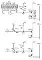
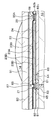
도 2는, 실시례 1의 촬상 소자의 등가 회로도.
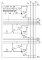
도 3은, 실시례 1의 촬상 소자의 등가 회로도.
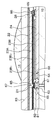
도 4는, 실시례 1의 촬상 소자를 구성하는 제1 전극 및 전하 축적용 전극 및 제어부를 구성하는 트랜지스터의 모식적인 배치도.
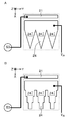
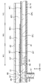
도 5는, 실시례 1의 촬상 소자의 동작시의 각 부위에서의 전위의 상태를 모식적으로 도시하는 도면.
도 6A, 도 6B 및 도 6C는, 도 5(실시례 1), 도 20 및 도 21(실시례 4) 및 도 32 및 도 33(실시례 6)의 각 부위를 설명하기 위한 실시례 1, 실시례 4 및 실시례 6의 촬상 소자의 등가 회로도.
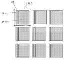
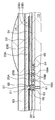
도 7은, 실시례 1의 촬상 소자를 구성하는 제1 전극 및 전하 축적용 전극의 모식적인 배치도.
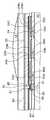
도 8은, 실시례 1의 촬상 소자를 구성하는 제1 전극, 전하 축적용 전극, 제2 전극 및 콘택트 홀부의 모식적인 투시 사시도.
도 9는, 실시례 1의 촬상 소자의 변형례의 등가 회로도.
도 10은, 도 9에 도시한 실시례 1의 촬상 소자의 변형례를 구성하는 제1 전극 및 전하 축적용 전극 및 제어부를 구성하는 트랜지스터의 모식적인 배치도.
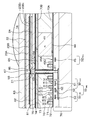
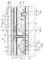
도 11은, 실시례 2의 촬상 소자의 모식적인 일부 단면도.
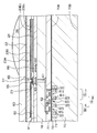
도 12는, 실시례 3의 촬상 소자의 모식적인 일부 단면도.
도 13은, 실시례 3의 촬상 소자의 변형례의 모식적인 일부 단면도.
도 14는, 실시례 3의 촬상 소자의 다른 변형례의 모식적인 일부 단면도.
도 15는, 실시례 3의 촬상 소자의 또 다른 변형례의 모식적인 일부 단면도.
도 16은, 실시례 4의 촬상 소자의 일부분의 모식적인 일부 단면도.
도 17은, 실시례 4의 촬상 소자의 등가 회로도.
도 18은, 실시례 4의 촬상 소자의 등가 회로도.
도 19는, 실시례 4의 촬상 소자를 구성하는 제1 전극, 전송 제어용 전극 및 전하 축적용 전극 및 제어부를 구성하는 트랜지스터의 모식적인 배치도.
도 20은, 실시례 4의 촬상 소자의 동작시의 각 부위에서의 전위의 상태를 모식적으로 도시하는 도면.
도 21은, 실시례 4의 촬상 소자의 다른 동작시의 각 부위에서의 전위의 상태를 모식적으로 도시하는 도면.
도 22는, 실시례 4의 촬상 소자를 구성하는 제1 전극, 전송 제어용 전극 및 전하 축적용 전극의 모식적인 배치도.
도 23은, 실시례 4의 촬상 소자를 구성하는 제1 전극, 전송 제어용 전극, 전하 축적용 전극, 제2 전극 및 콘택트 홀부의 모식적인 투시 사시도.
도 24는, 실시례 4의 촬상 소자의 변형례를 구성하는 제1 전극, 전송 제어용 전극 및 전하 축적용 전극 및 제어부를 구성하는 트랜지스터의 모식적인 배치도.
도 25는, 실시례 5의 촬상 소자의 일부분의 모식적인 일부 단면도.
도 26은, 실시례 5의 촬상 소자를 구성하는 제1 전극, 전하 축적용 전극 및 전하 배출 전극의 모식적인 배치도.
도 27은, 실시례 5의 촬상 소자를 구성하는 제1 전극, 전하 축적용 전극, 전하 배출 전극, 제2 전극 및 콘택트 홀부의 모식적인 투시 사시도.
도 28은, 실시례 6의 촬상 소자의 모식적인 일부 단면도.
도 29는, 실시례 6의 촬상 소자의 등가 회로도.
도 30은, 실시례 6의 촬상 소자의 등가 회로도.
도 31은, 실시례 6의 촬상 소자를 구성하는 제1 전극 및 전하 축적용 전극 및 제어부를 구성하는 트랜지스터의 모식적인 배치도.
도 32는, 실시례 6의 촬상 소자의 동작시의 각 부위에서의 전위의 상태를 모식적으로 도시하는 도면.
도 33은, 실시례 6의 촬상 소자의 다른 동작시(전송시)의 각 부위에서의 전위의 상태를 모식적으로 도시하는 도면.
도 34는, 실시례 6의 촬상 소자를 구성하는 제1 전극 및 전하 축적용 전극의 모식적인 배치도.
도 35는, 실시례 6의 촬상 소자를 구성하는 제1 전극, 전하 축적용 전극, 제2 전극 및 콘택트 홀부의 모식적인 투시 사시도.
도 36은, 실시례 6의 촬상 소자의 변형례를 구성하는 제1 전극 및 전하 축적용 전극의 모식적인 배치도.
도 37은, 실시례 7의 촬상 소자의 모식적인 일부 단면도.
도 38은, 실시례 7의 촬상 소자에서의 전하 축적용 전극, 광전변환층 및 제2 전극이 적층된 부분을 확대한 모식적인 일부 단면도.
도 39는, 실시례 7의 촬상 소자의 변형례를 구성하는 제1 전극 및 전하 축적용 전극 및 제어부를 구성하는 트랜지스터의 모식적인 배치도.
도 40은, 실시례 8의 촬상 소자에서의 전하 축적용 전극, 광전변환층 및 제2 전극이 적층된 부분을 확대한 모식적인 일부 단면도.
도 41은, 실시례 9의 촬상 소자의 모식적인 일부 단면도.
도 42는, 실시례 10 및 실시례 11의 촬상 소자의 모식적인 일부 단면도.
도 43A 및 도 43B는, 실시례 11에서의 전하 축적용 전극 세그먼트의 모식적인 평면도.
도 44A 및 도 44B는, 실시례 11에서의 전하 축적용 전극 세그먼트의 모식적인 평면도.
도 45는, 실시례 11의 촬상 소자를 구성하는 제1 전극 및 전하 축적용 전극 및 제어부를 구성하는 트랜지스터의 모식적인 배치도.
도 46은, 실시례 11의 촬상 소자의 변형례를 구성하는 제1 전극 및 전하 축적용 전극의 모식적인 배치도.
도 47은, 실시례 12 및 실시례 11의 촬상 소자의 모식적인 일부 단면도.
도 48A 및 도 48B는, 실시례 12에서의 전하 축적용 전극 세그먼트의 모식적인 평면도.
도 49는, 실시례 13의 고체 촬상 장치에서의 제1 전극 및 전하 축적용 전극 세그먼트의 모식적인 평면도.
도 50은, 실시례 13의 고체 촬상 장치의 제1 변형례에서의 제1 전극 및 전하 축적용 전극 세그먼트의 모식적인 평면도.
도 51은, 실시례 13의 고체 촬상 장치의 제2 변형례에서의 제1 전극 및 전하 축적용 전극 세그먼트의 모식적인 평면도.
도 52는, 실시례 13의 고체 촬상 장치의 제3 변형례에서의 제1 전극 및 전하 축적용 전극 세그먼트의 모식적인 평면도.
도 53은, 실시례 13의 고체 촬상 장치의 제4 변형례에서의 제1 전극 및 전하 축적용 전극 세그먼트의 모식적인 평면도.
도 54는, 실시례 13의 고체 촬상 장치의 제5 변형례에서의 제1 전극 및 전하 축적용 전극 세그먼트의 모식적인 평면도.
도 55는, 실시례 13의 고체 촬상 장치의 제6 변형례에서의 제1 전극 및 전하 축적용 전극 세그먼트의 모식적인 평면도.
도 56은, 실시례 13의 고체 촬상 장치의 제7 변형례에서의 제1 전극 및 전하 축적용 전극 세그먼트의 모식적인 평면도.
도 57은, 실시례 13의 고체 촬상 장치의 제8 변형례에서의 제1 전극 및 전하 축적용 전극 세그먼트의 모식적인 평면도.
도 58은, 실시례 13의 고체 촬상 장치의 제9 변형례에서의 제1 전극 및 전하 축적용 전극 세그먼트의 모식적인 평면도.
도 59A, 도 59B 및 도 59C는, 실시례 13의 촬상 소자 블록에서의 판독 구동례를 도시하는 차트.
도 60은, 실시례 14의 고체 촬상 장치에서의 제1 전극 및 전하 축적용 전극 세그먼트의 모식적인 평면도.
도 61은, 실시례 14의 고체 촬상 장치의 변형례에서의 제1 전극 및 전하 축적용 전극 세그먼트의 모식적인 평면도.
도 62는, 실시례 14의 고체 촬상 장치의 변형례에서의 제1 전극 및 전하 축적용 전극 세그먼트의 모식적인 평면도.
도 63은, 실시례 14의 고체 촬상 장치의 변형례에서의 제1 전극 및 전하 축적용 전극 세그먼트의 모식적인 평면도.
도 64는, 실시례 1의 촬상 소자의 다른 변형례의 모식적인 일부 단면도.
도 65는, 실시례 1의 촬상 소자의 또 다른 변형례의 모식적인 일부 단면도.
도 66A, 도 66B 및 도 66C는, 실시례 1의 촬상 소자의 또 다른 변형례의 제1 전극의 부분 등이 확대된 모식적인 일부 단면도.
도 67은, 실시례 5의 촬상 소자의 다른 변형례의 전하 배출 전극의 부분 등이 확대된 모식적인 일부 단면도.
도 68은, 실시례 1의 촬상 소자의 또 다른 변형례의 모식적인 일부 단면도.
도 69는, 실시례 1의 촬상 소자의 또 다른 변형례의 모식적인 일부 단면도.
도 70은, 실시례 1의 촬상 소자의 또 다른 변형례의 모식적인 일부 단면도.
도 71은, 실시례 4의 촬상 소자의 다른 변형례의 모식적인 일부 단면도.
도 72는, 실시례 1의 촬상 소자의 또 다른 변형례의 모식적인 일부 단면도.
도 73은, 실시례 4의 촬상 소자의 또 다른 변형례의 모식적인 일부 단면도.
도 74는, 실시례 7의 촬상 소자의 변형례에서의 전하 축적용 전극, 광전변환층 및 제2 전극이 적층된 부분을 확대한 모식적인 일부 단면도.
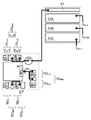
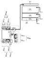
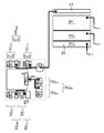
도 75는, 실시례 8의 촬상 소자의 변형례에서의 전하 축적용 전극, 광전변환층 및 제2 전극이 적층된 부분을 확대한 모식적인 일부 단면도.
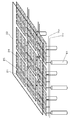
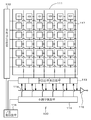
도 76은, 실시례 1의 고체 촬상 장치의 개념도.
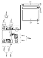
도 77은, 본 개시의 촬상 소자 등으로 구성된 고체 촬상 장치를 전자 기기(카메라)를 이용한 예의 개념도.
도 78은, 종래의 적층형 촬상 소자(적층형 고체 촬상 장치)의 개념도.

13 : 층간 절연층보다 하방에 위치하는 각종의 촬상 소자 구성 요소
14 : 온 칩·마이크로·렌즈(OCL)
15 : 차광층
21 : 제1 전극
22 : 제2 전극
23A : 광전변환층
23B : 복합산화물층
23B1 : 복합산화물층의 제1층
23B2 : 복합산화물층의 제2층
23'1, 23'2, 23'3 : 광전변환층 세그먼트
24, 24"1, 24"2, 24"3 : 전하 축적용 전극
24A, 24B, 24C, 24'1, 24'2, 24'3 : 전하 축적용 전극 세그먼트
25, 25A, 25B : 전송 제어용 전극(전하 전송 전극)
26 : 전하 배출 전극
27, 27A1, 27A2, 27A3, 27B1, 27B2, 27B3, 27C : 전하 이동 제어 전극,
31, 33, 41, 43 : n형 반도체 영역,
32, 34, 42, 44, 73 : p+층
35, 36, 45, 46 : 전송 트랜지스터의 게이트부
35C, 36C : 반도체 기판의 영역
36A : 전송 채널
51 : 리셋·트랜지스터(TR1rst)의 게이트부
51A : 리셋·트랜지스터(TR1rst)의 채널 형성 영역
51B, 51C : 리셋·트랜지스터(TR1rst)의 소스/드레인 영역
52 : 증폭 트랜지스터(TR1amp)의 게이트부
52A : 증폭 트랜지스터(TR1amp)의 채널 형성 영역
52B, 52C : 증폭 트랜지스터(TR1amp)의 소스/드레인 영역
53 : 선택 트랜지스터(TR1sel)의 게이트부
53A : 선택 트랜지스터(TR1sel)의 채널 형성 영역
53B, 53C : 선택 트랜지스터(TR1sel)의 소스/드레인 영역
61 : 콘택트 홀부
62 : 배선층
63, 64, 68A : 패드부
65, 68B : 접속구멍
66, 67, 69 : 접속부
70 : 반도체 기판
70A : 반도체 기판의 제1면(겉면)
70B : 반도체 기판의 제2면(이면)
71 : 소자 분리 영역
72 : 산화막
74 : HfO2막
75 : 절연 재료막
76, 81 : 층간 절연층
82 : 절연층
82'1, 82'2, 82'3 : 절연층 세그먼트
82a : 절연층의 제1면
82b : 절연층의 제2면
82c : 절연층의 제3면
83 : 절연층
85, 85A, 85B, 85C : 개구부
86, 86A : 제2 개구부
100 : 고체 촬상 장치
101 : 적층형 촬상 소자
111 : 촬상 영역
112 : 수직 구동 회로
113 : 칼럼 신호 처리 회로
114 : 수평 구동 회로
115 : 출력 회로
116 : 구동 제어 회로
117 : 신호선(데이터 출력선)
118 : 수평 신호선
200 : 전자 기기(카메라)
201 : 고체 촬상 장치
210 : 광학 렌즈
211 : 셔터 장치
212 : 구동 회로
213 : 신호 처리 회로
FD1, FD2, FD3, 45C, 46C : 부유 확산층
TR1trs, TR2trs, TR3trs : 전송 트랜지스터
TR1rst, TR2rst, TR3rst : 리셋·트랜지스터
TR1amp, TR2amp, TR3amp : 증폭 트랜지스터
TR1sel, TR3sel, TR3sel : 선택 트랜지스터
VDD : 전원
TG1, TG2, TG3 : 전송 게이트선
RST1, RST2, RST3 : 리셋선
SEL1, SEL2, SEL3 : 선택선
VSL, VSL1, VSL2, VSL3 : 신호선(데이터 출력선)
VOA, VOT, VOU : 배선
Claims (15)
- 제1 전극, 광전변환층 및 제2 전극이 적층되어 이루어지는 광전변환부를 구비하고 있고,
제1 전극과 광전변환층의 사이에는, 인듐복합산화물로 이루어지는 복합산화물층이 형성되어 있고,
복합산화물층은, 제1 전극에 인접한 제1층, 및, 광전변환층에 인접한 제2층을 구비하고 있고,
제1층에서의 인듐 조성은, 제2층에서의 인듐 조성보다도 높은 것을 특징으로 하는 촬상 소자. - 제1 전극, 광전변환층 및 제2 전극이 적층되어 이루어지는 광전변환부를 구비하고 있고,
제1 전극과 광전변환층의 사이에는, 인듐-갈륨-아연복합산화물로 이루어지는 복합산화물층이 형성되어 있고,
복합산화물층은, 제1 전극에 인접한 제1층, 및, 광전변환층에 인접한 제2층을 구비하고 있고,
제1층에서의 인듐 조성은, 제2층에서의 인듐 조성보다도 높고, 또는,
제1층에서의 갈륨 조성은, 제2층에서의 갈륨 조성보다도 낮고, 또는,
제1층에서의 아연 조성은, 제2층에서의 아연 조성보다도 높은 것을 특징으로 하는 촬상 소자. - 제2항에 있어서,
인듐-갈륨-아연복합산화물을 (ZnO)X(Ga2O3)1-X, (Ga2O3)Y(In2O3)1-Y 및 (In2O3)Z(ZnO)1-Z로 표시한 때,
제1층에서의 X의 값은 제2층에서의 X의 값보다도 높고, 또는,
제1층에서의 Y의 값은 제2층에서의 Y의 값보다도 낮고, 또는,
제1층에서의 Z의 값은 제2층에서의 Z의 값보다도 높은 것을 특징으로 하는 촬상 소자. - 제3항에 있어서,
0<X<0.875, 0<Y<0.875, 0.125<Z<0.875(단, X+Y+Z=1.000)를 만족하는 것을 특징으로 하는 촬상 소자. - 제1 전극, 광전변환층 및 제2 전극이 적층되어 이루어지는 광전변환부를 구비하고 있고,
제1 전극과 광전변환층의 사이에는, 인듐복합산화물로 이루어지는 복합산화물층이 형성되어 있고,
복합산화물층은, 제1 전극에 인접한 제1층, 및, 광전변환층에 인접한 제2층을 구비하고 있고,
제1층은, 제2층보다도 높은 캐리어 이동도를 갖는 것을 특징으로 하는 촬상 소자. - 제5항에 있어서,
1×10⁻⁶≤(제2층의 캐리어 이동도)/(제1층의 캐리어 이동도)≤0.1을 만족하는 것을 특징으로 하는 촬상 소자. - 제1 전극, 광전변환층 및 제2 전극이 적층되어 이루어지는 광전변환부를 구비하고 있고,
제1 전극과 광전변환층의 사이에는, 인듐복합산화물로 이루어지는 복합산화물층이 형성되어 있고,
복합산화물층은, 제1 전극에 인접한 제1층, 및, 광전변환층에 인접한 제2층을 구비하고 있고,
제1층은, 제2층보다도 낮은 상태밀도를 갖는 것을 특징으로 하는 촬상 소자. - 제1항, 제2항, 제5항 및 제7항 중 어느 한 항에 있어서,
복합산화물층은 비정질인 것을 특징으로 하는 촬상 소자. - 제1항, 제2항, 제5항 및 제7항 중 어느 한 항에 있어서,
광전변환부는, 또한, 절연층, 및, 제1 전극과 이간하여 배치되고, 또한, 절연층을 통하여 복합산화물층과 대향하여 배치된 전하 축적용 전극을 구비하고 있는 것을 특징으로 하는 촬상 소자. - 제9항에 있어서,
제1 전극과 전하 축적용 전극 사이에, 제1 전극 및 전하 축적용 전극과 이간하여 배치되고, 또한, 절연층을 통하여 복합산화물층과 대향하여 배치된 전송 제어용 전극을 또한 구비하고 있는 것을 특징으로 하는 촬상 소자. - 제9항에 있어서,
복합산화물층에 접속되고, 제1 전극 및 전하 축적용 전극과 이간하여 배치된 전하 배출 전극을 또한 구비하고 있는 것을 특징으로 하는 촬상 소자. - 제9항에 있어서,
전하 축적용 전극은, 복수의 전하 축적용 전극 세그먼트로 구성되어 있는 것을 특징으로 하는 촬상 소자. - 제1항 내지 제12항 중 어느 한 항에 기재된 촬상 소자를 적어도 하나 갖는 것을 특징으로 하는 적층형 촬상 소자.
- 제1항 내지 제12항 중 어느 한 항에 기재된 촬상 소자를, 복수, 구비한 것을 특징으로 하는 고체 촬상 장치.
- 제13항에 기재된 적층형 촬상 소자를, 복수, 구비한 것을 특징으로 하는 고체 촬상 장치.
Applications Claiming Priority (3)
| Application Number | Priority Date | Filing Date | Title |
|---|---|---|---|
| JPJP-P-2017-157143 | 2017-08-16 | ||
| JP2017157143 | 2017-08-16 | ||
| PCT/JP2018/018284 WO2019035252A1 (ja) | 2017-08-16 | 2018-05-11 | 撮像素子、積層型撮像素子及び固体撮像装置 |
Publications (2)
| Publication Number | Publication Date |
|---|---|
| KR20200035940A true KR20200035940A (ko) | 2020-04-06 |
| KR102552756B1 KR102552756B1 (ko) | 2023-07-07 |
Family
ID=65362887
Family Applications (1)
| Application Number | Title | Priority Date | Filing Date |
|---|---|---|---|
| KR1020207000827A Active KR102552756B1 (ko) | 2017-08-16 | 2018-05-11 | 촬상 소자, 적층형 촬상 소자 및 고체 촬상 장치 |
Country Status (7)
| Country | Link |
|---|---|
| US (1) | US11101303B2 (ko) |
| EP (1) | EP3671840A4 (ko) |
| JP (1) | JP7090087B2 (ko) |
| KR (1) | KR102552756B1 (ko) |
| CN (2) | CN111033740A (ko) |
| TW (1) | TWI784007B (ko) |
| WO (1) | WO2019035252A1 (ko) |
Cited By (1)
| Publication number | Priority date | Publication date | Assignee | Title |
|---|---|---|---|---|
| US12266674B2 (en) | 2020-08-18 | 2025-04-01 | Samsung Electronics Co, Ltd. | Image sensor with aluminum grid pattern having openings and copper dummy patterns covering the openings |
Families Citing this family (13)
| Publication number | Priority date | Publication date | Assignee | Title |
|---|---|---|---|---|
| EP3646381B1 (en) * | 2017-06-29 | 2023-05-31 | Sony Semiconductor Solutions Corporation | Wafer bonded back illuminated imager |
| JP2020088291A (ja) * | 2018-11-29 | 2020-06-04 | キヤノン株式会社 | 光電変換装置、光電変換システム、移動体 |
| US11164903B2 (en) | 2019-05-24 | 2021-11-02 | Taiwan Semiconductor Manufacturing Co., Ltd. | Image sensor with pad structure |
| US20220231245A1 (en) * | 2019-05-24 | 2022-07-21 | Sony Group Corporation | Imaging element, stacked imaging element and solid-state imaging device, and inorganic oxide semiconductor material |
| JP7559753B2 (ja) * | 2019-05-24 | 2024-10-02 | ソニーグループ株式会社 | 撮像素子、積層型撮像素子及び固体撮像装置、並びに、撮像素子の製造方法 |
| US11251210B2 (en) * | 2020-02-07 | 2022-02-15 | Sensors Unlimited, Inc. | Pin diodes with over-current protection |
| US11495631B2 (en) * | 2020-02-07 | 2022-11-08 | Sensors Unlimited, Inc. | Pin mesa diodes with over-current protection |
| JP7753193B2 (ja) * | 2020-03-31 | 2025-10-14 | ソニーセミコンダクタソリューションズ株式会社 | 撮像素子および撮像装置 |
| EP4131380A4 (en) * | 2020-03-31 | 2023-10-04 | Sony Group Corporation | Imaging element and imaging device |
| US20240355842A1 (en) * | 2021-09-10 | 2024-10-24 | Sony Semiconductor Solutions Corporation | Imaging element and imaging device |
| WO2023037622A1 (ja) * | 2021-09-10 | 2023-03-16 | ソニーセミコンダクタソリューションズ株式会社 | 撮像素子および撮像装置 |
| WO2024106235A1 (ja) * | 2022-11-15 | 2024-05-23 | ソニーセミコンダクタソリューションズ株式会社 | 光検出装置および光検出装置の製造方法ならびに電子機器 |
| WO2024202671A1 (ja) * | 2023-03-31 | 2024-10-03 | ソニーセミコンダクタソリューションズ株式会社 | 光検出装置および電子機器 |
Citations (4)
| Publication number | Priority date | Publication date | Assignee | Title |
|---|---|---|---|---|
| JP2011138927A (ja) | 2009-12-28 | 2011-07-14 | Sony Corp | 固体撮像装置とその製造方法、及び電子機器 |
| JP2014017374A (ja) * | 2012-07-09 | 2014-01-30 | Fujifilm Corp | 固体撮像素子および固体撮像素子の製造方法 |
| JP2016063165A (ja) | 2014-09-19 | 2016-04-25 | 株式会社東芝 | 撮像素子及び固体撮像装置 |
| KR20170031650A (ko) * | 2014-07-17 | 2017-03-21 | 소니 주식회사 | 광전 변환 소자, 촬상 장치, 광센서 및 광전 변환 소자의 제조 방법 |
Family Cites Families (11)
| Publication number | Priority date | Publication date | Assignee | Title |
|---|---|---|---|---|
| JP2007311647A (ja) * | 2006-05-19 | 2007-11-29 | Fujifilm Corp | 固体撮像素子 |
| JP2008177191A (ja) | 2007-01-16 | 2008-07-31 | Matsushita Electric Ind Co Ltd | 固体撮像装置およびそれを用いたカメラ |
| JP2011524463A (ja) * | 2008-05-06 | 2011-09-01 | エージェンシー フォー サイエンス,テクノロジー アンド リサーチ | 光透過性デバイス用導電性構造 |
| JP2013012556A (ja) * | 2011-06-28 | 2013-01-17 | Sony Corp | 固体撮像装置とその製造方法、および電子機器 |
| JP2012009910A (ja) * | 2011-10-14 | 2012-01-12 | Fujifilm Corp | 固体撮像素子 |
| JP6128020B2 (ja) * | 2013-04-10 | 2017-05-17 | ソニー株式会社 | 電子デバイス及び固体撮像装置、並びに、電子デバイスにおける電極形成方法 |
| JP6530664B2 (ja) | 2015-07-22 | 2019-06-12 | ソニーセミコンダクタソリューションズ株式会社 | 撮像装置及びその製造方法 |
| JP6780421B2 (ja) | 2016-03-01 | 2020-11-04 | ソニー株式会社 | 撮像素子、積層型撮像素子及び固体撮像装置、並びに、固体撮像装置の駆動方法 |
| US10580814B2 (en) * | 2016-03-15 | 2020-03-03 | Sony Corporation | Solid-state imaging device having light shielding films, method of manufacturing the same, and electronic apparatus |
| WO2017169757A1 (ja) * | 2016-03-29 | 2017-10-05 | ソニー株式会社 | 固体撮像素子およびその製造方法、並びに電子機器 |
| JP2018046039A (ja) * | 2016-09-12 | 2018-03-22 | ソニーセミコンダクタソリューションズ株式会社 | 固体撮像素子および固体撮像装置 |
-
2018
- 2018-05-11 WO PCT/JP2018/018284 patent/WO2019035252A1/ja not_active Ceased
- 2018-05-11 US US16/639,406 patent/US11101303B2/en active Active
- 2018-05-11 CN CN201880051512.7A patent/CN111033740A/zh active Pending
- 2018-05-11 EP EP18847126.2A patent/EP3671840A4/en active Pending
- 2018-05-11 JP JP2019536425A patent/JP7090087B2/ja active Active
- 2018-05-11 CN CN202411369008.5A patent/CN119277829A/zh active Pending
- 2018-05-11 KR KR1020207000827A patent/KR102552756B1/ko active Active
- 2018-06-07 TW TW107119575A patent/TWI784007B/zh active
Patent Citations (4)
| Publication number | Priority date | Publication date | Assignee | Title |
|---|---|---|---|---|
| JP2011138927A (ja) | 2009-12-28 | 2011-07-14 | Sony Corp | 固体撮像装置とその製造方法、及び電子機器 |
| JP2014017374A (ja) * | 2012-07-09 | 2014-01-30 | Fujifilm Corp | 固体撮像素子および固体撮像素子の製造方法 |
| KR20170031650A (ko) * | 2014-07-17 | 2017-03-21 | 소니 주식회사 | 광전 변환 소자, 촬상 장치, 광센서 및 광전 변환 소자의 제조 방법 |
| JP2016063165A (ja) | 2014-09-19 | 2016-04-25 | 株式会社東芝 | 撮像素子及び固体撮像装置 |
Cited By (1)
| Publication number | Priority date | Publication date | Assignee | Title |
|---|---|---|---|---|
| US12266674B2 (en) | 2020-08-18 | 2025-04-01 | Samsung Electronics Co, Ltd. | Image sensor with aluminum grid pattern having openings and copper dummy patterns covering the openings |
Also Published As
| Publication number | Publication date |
|---|---|
| TWI784007B (zh) | 2022-11-21 |
| CN119277829A (zh) | 2025-01-07 |
| KR102552756B1 (ko) | 2023-07-07 |
| EP3671840A1 (en) | 2020-06-24 |
| WO2019035252A1 (ja) | 2019-02-21 |
| TW201911550A (zh) | 2019-03-16 |
| EP3671840A4 (en) | 2020-08-19 |
| CN111033740A (zh) | 2020-04-17 |
| JPWO2019035252A1 (ja) | 2020-10-08 |
| US11101303B2 (en) | 2021-08-24 |
| JP7090087B2 (ja) | 2022-06-23 |
| US20200258923A1 (en) | 2020-08-13 |
Similar Documents
| Publication | Publication Date | Title |
|---|---|---|
| KR102628546B1 (ko) | 촬상 소자, 적층형 촬상 소자 및 고체 촬상 장치 | |
| KR102552756B1 (ko) | 촬상 소자, 적층형 촬상 소자 및 고체 촬상 장치 | |
| KR102595958B1 (ko) | 촬상 소자, 적층형 촬상 소자 및 고체 촬상 장치 | |
| KR102582170B1 (ko) | 촬상소자, 적층형 촬상소자 및 고체 촬상 장치 | |
| KR102734209B1 (ko) | 촬상 소자, 적층형 촬상 소자 및 고체 촬상 장치 | |
| KR102889822B1 (ko) | 촬상 소자, 적층형 촬상 소자 및 고체 촬상 장치 | |
| US20200295219A1 (en) | Imaging element, laminated imaging element, and solid-state imaging device | |
| KR102881384B1 (ko) | 촬상소자, 적층형 촬상소자 및 고체 촬상 장치 |
Legal Events
| Date | Code | Title | Description |
|---|---|---|---|
| PA0105 | International application |
Patent event date: 20200110 Patent event code: PA01051R01D Comment text: International Patent Application |
|
| PG1501 | Laying open of application | ||
| PA0201 | Request for examination |
Patent event code: PA02012R01D Patent event date: 20210413 Comment text: Request for Examination of Application |
|
| E902 | Notification of reason for refusal | ||
| PE0902 | Notice of grounds for rejection |
Comment text: Notification of reason for refusal Patent event date: 20221129 Patent event code: PE09021S01D |
|
| E701 | Decision to grant or registration of patent right | ||
| PE0701 | Decision of registration |
Patent event code: PE07011S01D Comment text: Decision to Grant Registration Patent event date: 20230403 |
|
| GRNT | Written decision to grant | ||
| PR0701 | Registration of establishment |
Comment text: Registration of Establishment Patent event date: 20230704 Patent event code: PR07011E01D |
|
| PR1002 | Payment of registration fee |
Payment date: 20230705 End annual number: 3 Start annual number: 1 |
|
| PG1601 | Publication of registration |