KR20200036697A - 센서 패키지 및 방법 - Google Patents
센서 패키지 및 방법 Download PDFInfo
- Publication number
- KR20200036697A KR20200036697A KR1020190056263A KR20190056263A KR20200036697A KR 20200036697 A KR20200036697 A KR 20200036697A KR 1020190056263 A KR1020190056263 A KR 1020190056263A KR 20190056263 A KR20190056263 A KR 20190056263A KR 20200036697 A KR20200036697 A KR 20200036697A
- Authority
- KR
- South Korea
- Prior art keywords
- sensor die
- dielectric layer
- opening
- redistribution structure
- die
- Prior art date
- Legal status (The legal status is an assumption and is not a legal conclusion. Google has not performed a legal analysis and makes no representation as to the accuracy of the status listed.)
- Granted
Links
Images













Classifications
-
- H—ELECTRICITY
- H10—SEMICONDUCTOR DEVICES; ELECTRIC SOLID-STATE DEVICES NOT OTHERWISE PROVIDED FOR
- H10W—GENERIC PACKAGES, INTERCONNECTIONS, CONNECTORS OR OTHER CONSTRUCTIONAL DETAILS OF DEVICES COVERED BY CLASS H10
- H10W74/00—Encapsulations, e.g. protective coatings
- H10W74/10—Encapsulations, e.g. protective coatings characterised by their shape or disposition
- H10W74/131—Encapsulations, e.g. protective coatings characterised by their shape or disposition the semiconductor body being only partially enclosed
- H10W74/137—Encapsulations, e.g. protective coatings characterised by their shape or disposition the semiconductor body being only partially enclosed the encapsulations being directly on the semiconductor body
-
- H—ELECTRICITY
- H10—SEMICONDUCTOR DEVICES; ELECTRIC SOLID-STATE DEVICES NOT OTHERWISE PROVIDED FOR
- H10P—GENERIC PROCESSES OR APPARATUS FOR THE MANUFACTURE OR TREATMENT OF DEVICES COVERED BY CLASS H10
- H10P72/00—Handling or holding of wafers, substrates or devices during manufacture or treatment thereof
- H10P72/70—Handling or holding of wafers, substrates or devices during manufacture or treatment thereof for supporting or gripping
- H10P72/74—Handling or holding of wafers, substrates or devices during manufacture or treatment thereof for supporting or gripping using temporarily an auxiliary support
-
- H—ELECTRICITY
- H10—SEMICONDUCTOR DEVICES; ELECTRIC SOLID-STATE DEVICES NOT OTHERWISE PROVIDED FOR
- H10W—GENERIC PACKAGES, INTERCONNECTIONS, CONNECTORS OR OTHER CONSTRUCTIONAL DETAILS OF DEVICES COVERED BY CLASS H10
- H10W20/00—Interconnections in chips, wafers or substrates
- H10W20/40—Interconnections external to wafers or substrates, e.g. back-end-of-line [BEOL] metallisations or vias connecting to gate electrodes
- H10W20/49—Adaptable interconnections, e.g. fuses or antifuses
-
- H01L23/525—
-
- H01L23/315—
-
- H01L23/481—
-
- H—ELECTRICITY
- H10—SEMICONDUCTOR DEVICES; ELECTRIC SOLID-STATE DEVICES NOT OTHERWISE PROVIDED FOR
- H10W—GENERIC PACKAGES, INTERCONNECTIONS, CONNECTORS OR OTHER CONSTRUCTIONAL DETAILS OF DEVICES COVERED BY CLASS H10
- H10W20/00—Interconnections in chips, wafers or substrates
- H10W20/20—Interconnections within wafers or substrates, e.g. through-silicon vias [TSV]
-
- H—ELECTRICITY
- H10—SEMICONDUCTOR DEVICES; ELECTRIC SOLID-STATE DEVICES NOT OTHERWISE PROVIDED FOR
- H10W—GENERIC PACKAGES, INTERCONNECTIONS, CONNECTORS OR OTHER CONSTRUCTIONAL DETAILS OF DEVICES COVERED BY CLASS H10
- H10W70/00—Package substrates; Interposers; Redistribution layers [RDL]
- H10W70/01—Manufacture or treatment
- H10W70/05—Manufacture or treatment of insulating or insulated package substrates, or of interposers, or of redistribution layers
- H10W70/08—Manufacture or treatment of insulating or insulated package substrates, or of interposers, or of redistribution layers by depositing layers on the chip or wafer, e.g. "chip-first" RDLs
- H10W70/09—Manufacture or treatment of insulating or insulated package substrates, or of interposers, or of redistribution layers by depositing layers on the chip or wafer, e.g. "chip-first" RDLs extending onto an encapsulation that laterally surrounds the chip or wafer, e.g. fan-out wafer level package [FOWLP] RDLs
-
- H—ELECTRICITY
- H10—SEMICONDUCTOR DEVICES; ELECTRIC SOLID-STATE DEVICES NOT OTHERWISE PROVIDED FOR
- H10W—GENERIC PACKAGES, INTERCONNECTIONS, CONNECTORS OR OTHER CONSTRUCTIONAL DETAILS OF DEVICES COVERED BY CLASS H10
- H10W70/00—Package substrates; Interposers; Redistribution layers [RDL]
- H10W70/60—Insulating or insulated package substrates; Interposers; Redistribution layers
-
- H—ELECTRICITY
- H10—SEMICONDUCTOR DEVICES; ELECTRIC SOLID-STATE DEVICES NOT OTHERWISE PROVIDED FOR
- H10W—GENERIC PACKAGES, INTERCONNECTIONS, CONNECTORS OR OTHER CONSTRUCTIONAL DETAILS OF DEVICES COVERED BY CLASS H10
- H10W72/00—Interconnections or connectors in packages
- H10W72/90—Bond pads, in general
-
- H—ELECTRICITY
- H10—SEMICONDUCTOR DEVICES; ELECTRIC SOLID-STATE DEVICES NOT OTHERWISE PROVIDED FOR
- H10W—GENERIC PACKAGES, INTERCONNECTIONS, CONNECTORS OR OTHER CONSTRUCTIONAL DETAILS OF DEVICES COVERED BY CLASS H10
- H10W74/00—Encapsulations, e.g. protective coatings
- H10W74/01—Manufacture or treatment
-
- H—ELECTRICITY
- H10—SEMICONDUCTOR DEVICES; ELECTRIC SOLID-STATE DEVICES NOT OTHERWISE PROVIDED FOR
- H10W—GENERIC PACKAGES, INTERCONNECTIONS, CONNECTORS OR OTHER CONSTRUCTIONAL DETAILS OF DEVICES COVERED BY CLASS H10
- H10W74/00—Encapsulations, e.g. protective coatings
- H10W74/01—Manufacture or treatment
- H10W74/014—Manufacture or treatment using batch processing
-
- H—ELECTRICITY
- H10—SEMICONDUCTOR DEVICES; ELECTRIC SOLID-STATE DEVICES NOT OTHERWISE PROVIDED FOR
- H10W—GENERIC PACKAGES, INTERCONNECTIONS, CONNECTORS OR OTHER CONSTRUCTIONAL DETAILS OF DEVICES COVERED BY CLASS H10
- H10W74/00—Encapsulations, e.g. protective coatings
- H10W74/01—Manufacture or treatment
- H10W74/016—Manufacture or treatment using moulds
-
- H—ELECTRICITY
- H10—SEMICONDUCTOR DEVICES; ELECTRIC SOLID-STATE DEVICES NOT OTHERWISE PROVIDED FOR
- H10W—GENERIC PACKAGES, INTERCONNECTIONS, CONNECTORS OR OTHER CONSTRUCTIONAL DETAILS OF DEVICES COVERED BY CLASS H10
- H10W74/00—Encapsulations, e.g. protective coatings
- H10W74/10—Encapsulations, e.g. protective coatings characterised by their shape or disposition
-
- H—ELECTRICITY
- H10—SEMICONDUCTOR DEVICES; ELECTRIC SOLID-STATE DEVICES NOT OTHERWISE PROVIDED FOR
- H10W—GENERIC PACKAGES, INTERCONNECTIONS, CONNECTORS OR OTHER CONSTRUCTIONAL DETAILS OF DEVICES COVERED BY CLASS H10
- H10W74/00—Encapsulations, e.g. protective coatings
- H10W74/10—Encapsulations, e.g. protective coatings characterised by their shape or disposition
- H10W74/111—Encapsulations, e.g. protective coatings characterised by their shape or disposition the semiconductor body being completely enclosed
- H10W74/124—Encapsulations, e.g. protective coatings characterised by their shape or disposition the semiconductor body being completely enclosed the encapsulations having cavities other than that occupied by chips
-
- H—ELECTRICITY
- H10—SEMICONDUCTOR DEVICES; ELECTRIC SOLID-STATE DEVICES NOT OTHERWISE PROVIDED FOR
- H10W—GENERIC PACKAGES, INTERCONNECTIONS, CONNECTORS OR OTHER CONSTRUCTIONAL DETAILS OF DEVICES COVERED BY CLASS H10
- H10W74/00—Encapsulations, e.g. protective coatings
- H10W74/10—Encapsulations, e.g. protective coatings characterised by their shape or disposition
- H10W74/131—Encapsulations, e.g. protective coatings characterised by their shape or disposition the semiconductor body being only partially enclosed
- H10W74/141—Encapsulations, e.g. protective coatings characterised by their shape or disposition the semiconductor body being only partially enclosed the encapsulations being on at least the sidewalls of the semiconductor body
-
- H01L2224/02379—
-
- H—ELECTRICITY
- H10—SEMICONDUCTOR DEVICES; ELECTRIC SOLID-STATE DEVICES NOT OTHERWISE PROVIDED FOR
- H10P—GENERIC PROCESSES OR APPARATUS FOR THE MANUFACTURE OR TREATMENT OF DEVICES COVERED BY CLASS H10
- H10P72/00—Handling or holding of wafers, substrates or devices during manufacture or treatment thereof
- H10P72/70—Handling or holding of wafers, substrates or devices during manufacture or treatment thereof for supporting or gripping
- H10P72/74—Handling or holding of wafers, substrates or devices during manufacture or treatment thereof for supporting or gripping using temporarily an auxiliary support
- H10P72/743—Handling or holding of wafers, substrates or devices during manufacture or treatment thereof for supporting or gripping using temporarily an auxiliary support used as a support during manufacture of interconnect decals or build up layers
-
- H—ELECTRICITY
- H10—SEMICONDUCTOR DEVICES; ELECTRIC SOLID-STATE DEVICES NOT OTHERWISE PROVIDED FOR
- H10P—GENERIC PROCESSES OR APPARATUS FOR THE MANUFACTURE OR TREATMENT OF DEVICES COVERED BY CLASS H10
- H10P72/00—Handling or holding of wafers, substrates or devices during manufacture or treatment thereof
- H10P72/70—Handling or holding of wafers, substrates or devices during manufacture or treatment thereof for supporting or gripping
- H10P72/74—Handling or holding of wafers, substrates or devices during manufacture or treatment thereof for supporting or gripping using temporarily an auxiliary support
- H10P72/7436—Handling or holding of wafers, substrates or devices during manufacture or treatment thereof for supporting or gripping using temporarily an auxiliary support used to support a device or a wafer when forming electrical connections thereto
-
- H—ELECTRICITY
- H10—SEMICONDUCTOR DEVICES; ELECTRIC SOLID-STATE DEVICES NOT OTHERWISE PROVIDED FOR
- H10P—GENERIC PROCESSES OR APPARATUS FOR THE MANUFACTURE OR TREATMENT OF DEVICES COVERED BY CLASS H10
- H10P72/00—Handling or holding of wafers, substrates or devices during manufacture or treatment thereof
- H10P72/70—Handling or holding of wafers, substrates or devices during manufacture or treatment thereof for supporting or gripping
- H10P72/74—Handling or holding of wafers, substrates or devices during manufacture or treatment thereof for supporting or gripping using temporarily an auxiliary support
- H10P72/744—Details of chemical or physical process used for separating the auxiliary support from a device or a wafer
-
- H—ELECTRICITY
- H10—SEMICONDUCTOR DEVICES; ELECTRIC SOLID-STATE DEVICES NOT OTHERWISE PROVIDED FOR
- H10W—GENERIC PACKAGES, INTERCONNECTIONS, CONNECTORS OR OTHER CONSTRUCTIONAL DETAILS OF DEVICES COVERED BY CLASS H10
- H10W70/00—Package substrates; Interposers; Redistribution layers [RDL]
- H10W70/60—Insulating or insulated package substrates; Interposers; Redistribution layers
- H10W70/62—Insulating or insulated package substrates; Interposers; Redistribution layers characterised by their interconnections
- H10W70/65—Shapes or dispositions of interconnections
-
- H—ELECTRICITY
- H10—SEMICONDUCTOR DEVICES; ELECTRIC SOLID-STATE DEVICES NOT OTHERWISE PROVIDED FOR
- H10W—GENERIC PACKAGES, INTERCONNECTIONS, CONNECTORS OR OTHER CONSTRUCTIONAL DETAILS OF DEVICES COVERED BY CLASS H10
- H10W70/00—Package substrates; Interposers; Redistribution layers [RDL]
- H10W70/60—Insulating or insulated package substrates; Interposers; Redistribution layers
- H10W70/62—Insulating or insulated package substrates; Interposers; Redistribution layers characterised by their interconnections
- H10W70/65—Shapes or dispositions of interconnections
- H10W70/654—Top-view layouts
- H10W70/655—Fan-out layouts
-
- H—ELECTRICITY
- H10—SEMICONDUCTOR DEVICES; ELECTRIC SOLID-STATE DEVICES NOT OTHERWISE PROVIDED FOR
- H10W—GENERIC PACKAGES, INTERCONNECTIONS, CONNECTORS OR OTHER CONSTRUCTIONAL DETAILS OF DEVICES COVERED BY CLASS H10
- H10W74/00—Encapsulations, e.g. protective coatings
- H10W74/01—Manufacture or treatment
- H10W74/019—Manufacture or treatment using temporary auxiliary substrates
Landscapes
- Internal Circuitry In Semiconductor Integrated Circuit Devices (AREA)
- Physics & Mathematics (AREA)
- Geometry (AREA)
Abstract
Description
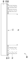
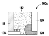
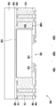
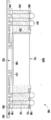
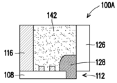
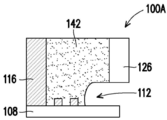
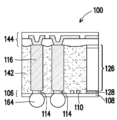
도 1, 2, 3, 4, 5a, 5b, 5c, 5d, 6, 7, 8, 9, 10, 및 11은 일부 실시예에 따라 센서 패키지를 형성하기 위한 공정 동안의 중간 단계들의 단면도를 묘사한다.
도 12, 13a, 13b, 13c, 13d, 14a, 14b, 14c, 및 14d는 일부 실시예에 따라 센서 패키지를 구현하는 감지 디바이스를 묘사한다.
도 15 내지 16은 일부 다른 실시예들에 따라 센서 패키지를 형성하기 위한 공정 동안의 중간 단계들의 단면도를 묘사한다.
도 17은 일부 실시예들에 따라 센서 패키지를 구현하는 감지 디바이스를 묘사한다.
도 18 내지 19는 일부 다른 실시예들에 따라 센서 패키지를 형성하기 위한 공정 동안의 중간 단계들의 단면도를 묘사한다.
도 20은 일부 실시예들에 따라 센서 패키지를 구현하는 감지 디바이스를 묘사한다.
도 21, 22, 및 22는 일부 다른 실시예들에 따라 센서 패키지를 구현하는 감지 디바이스를 묘사한다.
도 24a, 24b, 및 24c는 일부 실시예에 따라 패키지 컴포넌트를 묘사한다.
Claims (10)
- 디바이스에 있어서,
제1 표면과 상기 제1 표면의 반대쪽의 제2 표면을 갖는 센서 다이 - 상기 센서 다이는 상기 제1 표면에 입출력 영역과 제1 감지 영역을 가짐 -;
상기 센서 다이를 적어도 측방향으로 캡슐화하는 밀봉재;
상기 밀봉재를 관통해 연장되는 전도성 비아; 및
상기 센서 다이의 제1 표면 상의 전면 재배선 구조물
을 포함하고,
상기 전면 재배선 구조물은 상기 전도성 비아와 상기 센서 다이에 접속되고, 상기 전면 재배선 구조물은 상기 센서 다이의 입출력 영역을 덮으며, 상기 전면 재배선 구조물은 상기 센서 다이의 제1 감지 영역을 노출시키는 제1 개구를 가지는 것인, 디바이스. - 제1항에 있어서,
상기 센서 다이의 제2 표면 상에 후면 재배선 구조물을 더 포함하고, 상기 후면 재배선 구조물은 상기 전도성 비아에 접속되는 것인, 디바이스. - 제2항에 있어서,
상기 후면 재배선 구조물은,
유전체층; 및
상기 유전체층과 상기 밀봉재 사이에 배치된 금속화(metallization) 패턴을 포함하고, 상기 금속화 패턴은 상기 전도성 비아에 전기적으로 접속되는 것인, 디바이스. - 제2항에 있어서,
상기 센서 다이는 상기 제2 표면에 제2 감지 영역을 가지며, 상기 후면 재배선 구조물은 상기 센서 다이의 제2 감지 영역을 노출시키는 제2 개구를 갖는 것인, 디바이스. - 제4항에 있어서,
상기 제2 개구는 상기 밀봉재 내로 부분적으로 연장되고, 상기 센서 다이의 일부분의 측벽을 노출시키는 것인, 디바이스. - 제4항에 있어서,
상기 센서 다이의 일부분을 둘러싸는 접착제를 더 포함하고, 상기 제2 개구는 상기 접착제를 노출시키는 것인, 디바이스. - 제1항에 있어서,
상기 센서 다이는,
반도체 기판;
상기 반도체 기판 상의 패드 - 상기 패드는 상기 전면 재배선 구조물에 접속됨 -; 및
상기 패드 및 상기 반도체 기판 상의 패시베이션막을 포함하고, 상기 패시베이션막의 최상단 표면은 상기 밀봉재의 최상단 표면 위 또는 아래에 있는 것인, 디바이스. - 제1항에 있어서,
상기 센서 다이는,
반도체 기판;
상기 반도체 기판 상의 패드 - 상기 패드는 상기 전면 재배선 구조물에 접속됨 -;
상기 패드 및 상기 반도체 기판 상의 패시베이션막; 및
상기 패시베이션막 위의 유전체층
을 포함하고,
상기 유전체층은 상기 센서 다이의 제1 감지 영역을 노출시키는 제2 개구를 가지며, 상기 제2 개구의 폭은 상기 제1 개구의 폭보다 작은 것인, 디바이스. - 방법에 있어서,
전도성 비아에 인접하게 센서 다이를 배치하는 단계 - 상기 센서 다이는 입출력 영역과 제1 감지 영역을 가짐 -;
상기 센서 다이와 상기 전도성 비아를 밀봉재로 캡슐화하는 단계;
상기 밀봉재, 상기 센서 다이, 및 상기 전도성 비아 상에 제1 유전체층을 형성하는 단계;
상기 전도성 비아를 노출시키는 제1 개구, 상기 센서 다이의 입출력 영역을 노출시키는 제2 개구, 및 상기 센서 다이의 제1 감지 영역을 노출시키는 제3 개구를 갖는 상기 제1 유전체층을 패터닝하는 단계;
상기 제1 유전체층의 제1 개구 및 제2 개구를 관통해 연장되는 제1 금속화 패턴을 형성하는 단계 - 상기 제1 유전체층의 제3 개구에는 상기 제1 금속화 패턴이 없음 -;
상기 제1 금속화 패턴과 상기 제1 유전체층 상에 제2 유전체층을 형성하는 단계; 및
상기 센서 다이의 제1 감지 영역을 노출시키도록 상기 제2 유전체층을 관통해 상기 제3 개구를 연장하는 단계
를 포함하는, 방법. - 방법에 있어서,
후면 재배선 구조물을 형성하는 단계 - 상기 후면 재배선 구조물은 제1 개구를 가짐 -;
접착제를 사용해 상기 후면 재배선 구조물의 제1 개구 내에 센서 다이를 접착시키는 단계 - 상기 센서 다이는 제1 표면과 상기 제1 표면의 반대쪽의 제2 표면을 가짐 -;
밀봉재를 사용해 상기 센서 다이를 캡슐화하는 단계;
상기 밀봉재와 상기 센서 다이 위에 전면 재배선 구조물을 형성하는 단계 - 상기 전면 재배선 구조물은 상기 센서 다이의 제2 표면을 노출시키는 제2 개구를 가짐 -; 및
상기 전면 재배선 구조물을 형성하는 단계 후에, 상기 센서 다이의 제1 표면을 노출시키도록 상기 접착제를 제거하는 단계
를 포함하는, 방법.
Applications Claiming Priority (4)
| Application Number | Priority Date | Filing Date | Title |
|---|---|---|---|
| US201862737282P | 2018-09-27 | 2018-09-27 | |
| US62/737,282 | 2018-09-27 | ||
| US16/266,276 | 2019-02-04 | ||
| US16/266,276 US10832985B2 (en) | 2018-09-27 | 2019-02-04 | Sensor package and method |
Publications (2)
| Publication Number | Publication Date |
|---|---|
| KR20200036697A true KR20200036697A (ko) | 2020-04-07 |
| KR102296825B1 KR102296825B1 (ko) | 2021-09-02 |
Family
ID=69946098
Family Applications (1)
| Application Number | Title | Priority Date | Filing Date |
|---|---|---|---|
| KR1020190056263A Active KR102296825B1 (ko) | 2018-09-27 | 2019-05-14 | 센서 패키지 및 방법 |
Country Status (4)
| Country | Link |
|---|---|
| US (2) | US10832985B2 (ko) |
| KR (1) | KR102296825B1 (ko) |
| CN (1) | CN110957229B (ko) |
| TW (1) | TWI718606B (ko) |
Cited By (2)
| Publication number | Priority date | Publication date | Assignee | Title |
|---|---|---|---|---|
| KR20210135414A (ko) * | 2020-05-04 | 2021-11-15 | 타이완 세미콘덕터 매뉴팩쳐링 컴퍼니 리미티드 | 센서 패키지 및 방법 |
| KR20230117688A (ko) * | 2022-01-31 | 2023-08-09 | 타이완 세미콘덕터 매뉴팩쳐링 컴퍼니 리미티드 | 통합 광학 다이를 구비한 패키지 및 그 형성 방법 |
Families Citing this family (21)
| Publication number | Priority date | Publication date | Assignee | Title |
|---|---|---|---|---|
| US11626448B2 (en) | 2019-03-29 | 2023-04-11 | Lumileds Llc | Fan-out light-emitting diode (LED) device substrate with embedded backplane, lighting system and method of manufacture |
| CN112574668A (zh) * | 2019-09-27 | 2021-03-30 | 台湾积体电路制造股份有限公司 | 用于牺牲膜的组合物 |
| US11798857B2 (en) * | 2019-09-27 | 2023-10-24 | Taiwan Semiconductor Manufacturing Company, Ltd. | Composition for sacrificial film, package, manufacturing method of package |
| US11289396B2 (en) * | 2019-09-29 | 2022-03-29 | Taiwan Semiconductor Manufacturing Company, Ltd. | Sensing component encapsulated by an encapsulation layer with a roughness surface having a hollow region |
| US11621173B2 (en) | 2019-11-19 | 2023-04-04 | Lumileds Llc | Fan out structure for light-emitting diode (LED) device and lighting system |
| US11777066B2 (en) | 2019-12-27 | 2023-10-03 | Lumileds Llc | Flipchip interconnected light-emitting diode package assembly |
| US11664347B2 (en) | 2020-01-07 | 2023-05-30 | Lumileds Llc | Ceramic carrier and build up carrier for light-emitting diode (LED) array |
| US11476217B2 (en) | 2020-03-10 | 2022-10-18 | Lumileds Llc | Method of manufacturing an augmented LED array assembly |
| DE102020126648A1 (de) * | 2020-05-18 | 2021-11-18 | Taiwan Semiconductor Manufacturing Co., Ltd. | Umverteilungsstruktur für integrierte-schaltung-package und deren herstellungsverfahren |
| US12113022B2 (en) * | 2020-05-26 | 2024-10-08 | Taiwan Semiconductor Manufacturing Company, Ltd. | Semiconductor package and manufacturing method of semiconductor package |
| US11527518B2 (en) | 2020-07-27 | 2022-12-13 | Taiwan Semiconductor Manufacturing Co., Ltd. | Heat dissipation in semiconductor packages and methods of forming same |
| US11587899B2 (en) * | 2020-07-29 | 2023-02-21 | Texas Instruments Incorporated | Multi-layer semiconductor package with stacked passive components |
| CN112103268B (zh) * | 2020-08-05 | 2021-08-03 | 珠海越亚半导体股份有限公司 | 一种嵌入式封装结构及其制造方法 |
| CN115472636A (zh) * | 2021-06-11 | 2022-12-13 | 群创光电股份有限公司 | 感测装置以及电子装置 |
| US12051655B2 (en) * | 2021-07-16 | 2024-07-30 | Taiwan Semiconductor Manufacturing Company, Ltd. | Package structure and method of forming the same |
| US12009226B2 (en) * | 2021-08-27 | 2024-06-11 | Taiwan Semiconductor Manufacturing Co., Ltd. | Semiconductor device and method of forming same |
| US12261088B2 (en) * | 2021-08-31 | 2025-03-25 | Taiwan Semiconductor Manufacturing Company, Ltd. | Package structure and method of forming the same |
| US11908764B2 (en) * | 2021-08-31 | 2024-02-20 | Taiwan Semiconductor Manufacturing Company, Ltd. | Semiconductor package including a circuit substrate having a cavity and a floor plate embedded in a dielectric material and a semiconductor die disposed in the cavity |
| US20230253281A1 (en) * | 2022-02-09 | 2023-08-10 | Texas Instruments Incorporated | Sensor package with cavity created using sacrificial material |
| US20240030115A1 (en) * | 2022-07-22 | 2024-01-25 | Stmicroelectronics Pte Ltd | Power package with copper plating and molding structure |
| KR20250068002A (ko) * | 2023-11-08 | 2025-05-16 | 에스케이하이닉스 주식회사 | 서로 다른 봉지층들을 갖는 반도체 패키지 |
Citations (3)
| Publication number | Priority date | Publication date | Assignee | Title |
|---|---|---|---|---|
| KR20170094483A (ko) * | 2016-02-10 | 2017-08-18 | 타이완 세미콘덕터 매뉴팩쳐링 컴퍼니 리미티드 | 지문 센서 픽셀 어레이 및 이의 형성 방법 |
| KR20170101092A (ko) * | 2016-02-26 | 2017-09-05 | 타이완 세미콘덕터 매뉴팩쳐링 컴퍼니 리미티드 | 지문 센서 소자 및 방법 |
| KR20180004062A (ko) * | 2017-12-27 | 2018-01-10 | 주식회사 네패스 | 센서 패키지 및 이의 제조 방법 |
Family Cites Families (37)
| Publication number | Priority date | Publication date | Assignee | Title |
|---|---|---|---|---|
| US20080191297A1 (en) | 2007-02-12 | 2008-08-14 | Advanced Chip Engineering Technology Inc. | Wafer level image sensor package with die receiving cavity and method of the same |
| US8759964B2 (en) | 2007-07-17 | 2014-06-24 | Taiwan Semiconductor Manufacturing Company, Ltd. | Wafer level package structure and fabrication methods |
| SG152086A1 (en) * | 2007-10-23 | 2009-05-29 | Micron Technology Inc | Packaged semiconductor assemblies and associated systems and methods |
| US8263434B2 (en) | 2009-07-31 | 2012-09-11 | Stats Chippac, Ltd. | Semiconductor device and method of mounting die with TSV in cavity of substrate for electrical interconnect of Fi-PoP |
| US9324672B2 (en) * | 2009-08-21 | 2016-04-26 | Stats Chippac, Ltd. | Semiconductor device and method of forming dual-active sided semiconductor die in fan-out wafer level chip scale package |
| JP5423880B2 (ja) | 2010-04-07 | 2014-02-19 | 株式会社島津製作所 | 放射線検出器およびそれを製造する方法 |
| US9048233B2 (en) | 2010-05-26 | 2015-06-02 | Taiwan Semiconductor Manufacturing Company, Ltd. | Package systems having interposers |
| US8361842B2 (en) | 2010-07-30 | 2013-01-29 | Taiwan Semiconductor Manufacturing Company, Ltd. | Embedded wafer-level bonding approaches |
| US8884431B2 (en) | 2011-09-09 | 2014-11-11 | Taiwan Semiconductor Manufacturing Company, Ltd. | Packaging methods and structures for semiconductor devices |
| US9064879B2 (en) | 2010-10-14 | 2015-06-23 | Taiwan Semiconductor Manufacturing Company, Ltd. | Packaging methods and structures using a die attach film |
| US8829676B2 (en) | 2011-06-28 | 2014-09-09 | Taiwan Semiconductor Manufacturing Company, Ltd. | Interconnect structure for wafer level package |
| CN102903722A (zh) | 2011-07-26 | 2013-01-30 | 旭丽电子(广州)有限公司 | 薄型化有源检测模块及其制作方法 |
| US9018725B2 (en) * | 2011-09-02 | 2015-04-28 | Optiz, Inc. | Stepped package for image sensor and method of making same |
| US9000584B2 (en) | 2011-12-28 | 2015-04-07 | Taiwan Semiconductor Manufacturing Company, Ltd. | Packaged semiconductor device with a molding compound and a method of forming the same |
| US8680647B2 (en) | 2011-12-29 | 2014-03-25 | Taiwan Semiconductor Manufacturing Company, Ltd. | Packages with passive devices and methods of forming the same |
| US8703542B2 (en) | 2012-05-18 | 2014-04-22 | Taiwan Semiconductor Manufacturing Company, Ltd. | Wafer-level packaging mechanisms |
| US9991190B2 (en) | 2012-05-18 | 2018-06-05 | Taiwan Semiconductor Manufacturing Company, Ltd. | Packaging with interposer frame |
| US8809996B2 (en) | 2012-06-29 | 2014-08-19 | Taiwan Semiconductor Manufacturing Company, Ltd. | Package with passive devices and method of forming the same |
| US8653626B2 (en) * | 2012-07-18 | 2014-02-18 | Taiwan Semiconductor Manufacturing Company, Ltd. | Package structures including a capacitor and methods of forming the same |
| US8785299B2 (en) | 2012-11-30 | 2014-07-22 | Taiwan Semiconductor Manufacturing Company, Ltd. | Package with a fan-out structure and method of forming the same |
| US8803306B1 (en) | 2013-01-18 | 2014-08-12 | Taiwan Semiconductor Manufacturing Company, Ltd. | Fan-out package structure and methods for forming the same |
| US8778738B1 (en) | 2013-02-19 | 2014-07-15 | Taiwan Semiconductor Manufacturing Company, Ltd. | Packaged semiconductor devices and packaging devices and methods |
| US9035461B2 (en) * | 2013-01-30 | 2015-05-19 | Taiwan Semiconductor Manufacturing Company, Ltd. | Packaged semiconductor devices and packaging methods |
| US9299649B2 (en) * | 2013-02-08 | 2016-03-29 | Taiwan Semiconductor Manufacturing Company, Ltd. | 3D packages and methods for forming the same |
| US9263511B2 (en) | 2013-02-11 | 2016-02-16 | Taiwan Semiconductor Manufacturing Co., Ltd. | Package with metal-insulator-metal capacitor and method of manufacturing the same |
| KR102063817B1 (ko) * | 2013-03-04 | 2020-01-08 | 삼성전자주식회사 | 반도체 패키지를 포함하는 반도체 장치의 표면 온도 제어 방법 |
| US9048222B2 (en) * | 2013-03-06 | 2015-06-02 | Taiwan Semiconductor Manufacturing Company, Ltd. | Method of fabricating interconnect structure for package-on-package devices |
| US9368460B2 (en) | 2013-03-15 | 2016-06-14 | Taiwan Semiconductor Manufacturing Company, Ltd. | Fan-out interconnect structure and method for forming same |
| US8877554B2 (en) | 2013-03-15 | 2014-11-04 | Taiwan Semiconductor Manufacturing Company, Ltd. | Packaged semiconductor devices, methods of packaging semiconductor devices, and PoP devices |
| TWI538174B (zh) * | 2013-09-25 | 2016-06-11 | 晶相光電股份有限公司 | 半導體裝置的製造方法 |
| US9527723B2 (en) * | 2014-03-13 | 2016-12-27 | STATS ChipPAC Pte. Ltd. | Semiconductor device and method of forming microelectromechanical systems (MEMS) package |
| US9543170B2 (en) * | 2014-08-22 | 2017-01-10 | Taiwan Semiconductor Manufacturing Company, Ltd. | Semiconductor packages and methods of forming the same |
| US9812337B2 (en) * | 2014-12-03 | 2017-11-07 | Taiwan Semiconductor Manufacturing Company, Ltd. | Integrated circuit package pad and methods of forming |
| CN105845639B (zh) | 2015-01-16 | 2019-03-19 | 恒劲科技股份有限公司 | 电子封装结构及导电结构 |
| US9847269B2 (en) * | 2015-07-31 | 2017-12-19 | Taiwan Semiconductor Manufacturing Company, Ltd. | Fan-out packages and methods of forming same |
| US9929112B2 (en) * | 2015-09-25 | 2018-03-27 | Taiwan Semiconductor Manufacturing Company, Ltd. | Semiconductor device and method of manufacture |
| US9691708B1 (en) | 2016-07-20 | 2017-06-27 | Taiwan Semiconductor Manufacturing Co., Ltd. | Semiconductor package and manufacturing method thereof |
-
2019
- 2019-02-04 US US16/266,276 patent/US10832985B2/en active Active
- 2019-05-14 KR KR1020190056263A patent/KR102296825B1/ko active Active
- 2019-07-31 TW TW108127160A patent/TWI718606B/zh active
- 2019-09-25 CN CN201910912553.7A patent/CN110957229B/zh active Active
-
2020
- 2020-11-09 US US17/092,543 patent/US11742254B2/en active Active
Patent Citations (3)
| Publication number | Priority date | Publication date | Assignee | Title |
|---|---|---|---|---|
| KR20170094483A (ko) * | 2016-02-10 | 2017-08-18 | 타이완 세미콘덕터 매뉴팩쳐링 컴퍼니 리미티드 | 지문 센서 픽셀 어레이 및 이의 형성 방법 |
| KR20170101092A (ko) * | 2016-02-26 | 2017-09-05 | 타이완 세미콘덕터 매뉴팩쳐링 컴퍼니 리미티드 | 지문 센서 소자 및 방법 |
| KR20180004062A (ko) * | 2017-12-27 | 2018-01-10 | 주식회사 네패스 | 센서 패키지 및 이의 제조 방법 |
Cited By (5)
| Publication number | Priority date | Publication date | Assignee | Title |
|---|---|---|---|---|
| KR20210135414A (ko) * | 2020-05-04 | 2021-11-15 | 타이완 세미콘덕터 매뉴팩쳐링 컴퍼니 리미티드 | 센서 패키지 및 방법 |
| TWI796618B (zh) * | 2020-05-04 | 2023-03-21 | 台灣積體電路製造股份有限公司 | 半導體裝置、半導體封裝及形成半導體裝置的方法 |
| US11942417B2 (en) | 2020-05-04 | 2024-03-26 | Taiwan Semiconductor Manufacturing Co., Ltd. | Sensor package and method |
| KR20230117688A (ko) * | 2022-01-31 | 2023-08-09 | 타이완 세미콘덕터 매뉴팩쳐링 컴퍼니 리미티드 | 통합 광학 다이를 구비한 패키지 및 그 형성 방법 |
| US12228776B2 (en) | 2022-01-31 | 2025-02-18 | Taiwan Semiconductor Manufacturing Co., Ltd. | Package with integrated optical die and method forming same |
Also Published As
| Publication number | Publication date |
|---|---|
| CN110957229A (zh) | 2020-04-03 |
| US20200105638A1 (en) | 2020-04-02 |
| KR102296825B1 (ko) | 2021-09-02 |
| US20210057302A1 (en) | 2021-02-25 |
| CN110957229B (zh) | 2021-08-24 |
| TWI718606B (zh) | 2021-02-11 |
| US10832985B2 (en) | 2020-11-10 |
| TW202013660A (zh) | 2020-04-01 |
| US11742254B2 (en) | 2023-08-29 |
Similar Documents
| Publication | Publication Date | Title |
|---|---|---|
| KR102296825B1 (ko) | 센서 패키지 및 방법 | |
| US20220320029A1 (en) | Dummy Structure of Stacked and Bonded Semiconductor Device | |
| KR102108236B1 (ko) | 반도체 패키지들 내의 금속화 패턴들 및 그 형성 방법들 | |
| TWI652786B (zh) | 半導體封裝及其形成方法 | |
| TWI790503B (zh) | 積體電路封裝及其形成方法 | |
| KR102484495B1 (ko) | 디바이스, 패키지 및 방법 | |
| US20180269188A1 (en) | Semiconductor packages and methods of forming same | |
| US20180122774A1 (en) | Redistribution Layers in Semiconductor Packages and Methods of Forming Same | |
| CN110034026A (zh) | 封装件结构和方法 | |
| KR20200037051A (ko) | 집적 회로 패키지 및 방법 | |
| US12205860B2 (en) | Sensor packages | |
| KR20210134868A (ko) | 반도체 패키지 및 그 제조 방법 | |
| TW201816897A (zh) | 半導體封裝中的密集型重佈線層以及其形成方法 | |
| CN108269767A (zh) | 衬底晶片上芯片结构的形成方法 | |
| TW201924007A (zh) | 半導體元件及其形成方法 | |
| CN113140516A (zh) | 封装件及其形成方法 | |
| TW202008481A (zh) | 形成半導體封裝體的方法 | |
| KR102557597B1 (ko) | 반도체 패키징 및 그 형성 방법 | |
| US12381163B2 (en) | Semiconductor package and manufacturing method thereof | |
| CN112542449B (zh) | 半导体器件及其制造方法 | |
| TW202141709A (zh) | 半導體封裝體及其製造方法 | |
| TWI905705B (zh) | 積體電路封裝件及其形成方法 |
Legal Events
| Date | Code | Title | Description |
|---|---|---|---|
| PA0109 | Patent application |
St.27 status event code: A-0-1-A10-A12-nap-PA0109 |
|
| PA0201 | Request for examination |
St.27 status event code: A-1-2-D10-D11-exm-PA0201 |
|
| R18-X000 | Changes to party contact information recorded |
St.27 status event code: A-3-3-R10-R18-oth-X000 |
|
| PG1501 | Laying open of application |
St.27 status event code: A-1-1-Q10-Q12-nap-PG1501 |
|
| D13-X000 | Search requested |
St.27 status event code: A-1-2-D10-D13-srh-X000 |
|
| D14-X000 | Search report completed |
St.27 status event code: A-1-2-D10-D14-srh-X000 |
|
| E902 | Notification of reason for refusal | ||
| PE0902 | Notice of grounds for rejection |
St.27 status event code: A-1-2-D10-D21-exm-PE0902 |
|
| T11-X000 | Administrative time limit extension requested |
St.27 status event code: U-3-3-T10-T11-oth-X000 |
|
| T11-X000 | Administrative time limit extension requested |
St.27 status event code: U-3-3-T10-T11-oth-X000 |
|
| T11-X000 | Administrative time limit extension requested |
St.27 status event code: U-3-3-T10-T11-oth-X000 |
|
| P11-X000 | Amendment of application requested |
St.27 status event code: A-2-2-P10-P11-nap-X000 |
|
| P13-X000 | Application amended |
St.27 status event code: A-2-2-P10-P13-nap-X000 |
|
| E701 | Decision to grant or registration of patent right | ||
| PE0701 | Decision of registration |
St.27 status event code: A-1-2-D10-D22-exm-PE0701 |
|
| GRNT | Written decision to grant | ||
| PR0701 | Registration of establishment |
St.27 status event code: A-2-4-F10-F11-exm-PR0701 |
|
| PR1002 | Payment of registration fee |
St.27 status event code: A-2-2-U10-U11-oth-PR1002 Fee payment year number: 1 |
|
| PG1601 | Publication of registration |
St.27 status event code: A-4-4-Q10-Q13-nap-PG1601 |
|
| PR1001 | Payment of annual fee |
St.27 status event code: A-4-4-U10-U11-oth-PR1001 Fee payment year number: 4 |
|
| PR1001 | Payment of annual fee |
St.27 status event code: A-4-4-U10-U11-oth-PR1001 Fee payment year number: 5 |
|
| U11 | Full renewal or maintenance fee paid |
Free format text: ST27 STATUS EVENT CODE: A-4-4-U10-U11-OTH-PR1001 (AS PROVIDED BY THE NATIONAL OFFICE) Year of fee payment: 5 |
|
| P22-X000 | Classification modified |
St.27 status event code: A-4-4-P10-P22-nap-X000 |
|
| P22-X000 | Classification modified |
St.27 status event code: A-4-4-P10-P22-nap-X000 |