KR20200036744A - 프로브 카드 지지장치 - Google Patents
프로브 카드 지지장치 Download PDFInfo
- Publication number
- KR20200036744A KR20200036744A KR1020190111533A KR20190111533A KR20200036744A KR 20200036744 A KR20200036744 A KR 20200036744A KR 1020190111533 A KR1020190111533 A KR 1020190111533A KR 20190111533 A KR20190111533 A KR 20190111533A KR 20200036744 A KR20200036744 A KR 20200036744A
- Authority
- KR
- South Korea
- Prior art keywords
- probe card
- card
- support
- edge
- shaped member
- Prior art date
- Legal status (The legal status is an assumption and is not a legal conclusion. Google has not performed a legal analysis and makes no representation as to the accuracy of the status listed.)
- Granted
Links
- 239000000523 sample Substances 0.000 claims abstract description 188
- 238000007689 inspection Methods 0.000 description 15
- 238000010586 diagram Methods 0.000 description 6
- 230000008878 coupling Effects 0.000 description 3
- 238000010168 coupling process Methods 0.000 description 3
- 238000005859 coupling reaction Methods 0.000 description 3
- 230000000694 effects Effects 0.000 description 3
- 239000004065 semiconductor Substances 0.000 description 3
- 230000007423 decrease Effects 0.000 description 1
- 230000007547 defect Effects 0.000 description 1
- 238000012423 maintenance Methods 0.000 description 1
- 229920003002 synthetic resin Polymers 0.000 description 1
- 239000000057 synthetic resin Substances 0.000 description 1
Images



Classifications
-
- G—PHYSICS
- G01—MEASURING; TESTING
- G01R—MEASURING ELECTRIC VARIABLES; MEASURING MAGNETIC VARIABLES
- G01R1/00—Details of instruments or arrangements of the types included in groups G01R5/00 - G01R13/00 and G01R31/00
- G01R1/02—General constructional details
- G01R1/04—Housings; Supporting members; Arrangements of terminals
- G01R1/0408—Test fixtures or contact fields; Connectors or connecting adaptors; Test clips; Test sockets
-
- G—PHYSICS
- G01—MEASURING; TESTING
- G01R—MEASURING ELECTRIC VARIABLES; MEASURING MAGNETIC VARIABLES
- G01R1/00—Details of instruments or arrangements of the types included in groups G01R5/00 - G01R13/00 and G01R31/00
- G01R1/02—General constructional details
- G01R1/06—Measuring leads; Measuring probes
- G01R1/067—Measuring probes
- G01R1/073—Multiple probes
- G01R1/07307—Multiple probes with individual probe elements, e.g. needles, cantilever beams or bump contacts, fixed in relation to each other, e.g. bed of nails fixture or probe card
- G01R1/07342—Multiple probes with individual probe elements, e.g. needles, cantilever beams or bump contacts, fixed in relation to each other, e.g. bed of nails fixture or probe card the body of the probe being at an angle other than perpendicular to test object, e.g. probe card
-
- G—PHYSICS
- G01—MEASURING; TESTING
- G01R—MEASURING ELECTRIC VARIABLES; MEASURING MAGNETIC VARIABLES
- G01R1/00—Details of instruments or arrangements of the types included in groups G01R5/00 - G01R13/00 and G01R31/00
- G01R1/02—General constructional details
- G01R1/04—Housings; Supporting members; Arrangements of terminals
-
- G—PHYSICS
- G01—MEASURING; TESTING
- G01R—MEASURING ELECTRIC VARIABLES; MEASURING MAGNETIC VARIABLES
- G01R1/00—Details of instruments or arrangements of the types included in groups G01R5/00 - G01R13/00 and G01R31/00
- G01R1/02—General constructional details
- G01R1/04—Housings; Supporting members; Arrangements of terminals
- G01R1/0408—Test fixtures or contact fields; Connectors or connecting adaptors; Test clips; Test sockets
- G01R1/0491—Test fixtures or contact fields; Connectors or connecting adaptors; Test clips; Test sockets for testing integrated circuits on wafers, e.g. wafer-level test cartridge
-
- G—PHYSICS
- G01—MEASURING; TESTING
- G01R—MEASURING ELECTRIC VARIABLES; MEASURING MAGNETIC VARIABLES
- G01R1/00—Details of instruments or arrangements of the types included in groups G01R5/00 - G01R13/00 and G01R31/00
- G01R1/02—General constructional details
- G01R1/06—Measuring leads; Measuring probes
- G01R1/067—Measuring probes
- G01R1/06788—Hand-held or hand-manipulated probes, e.g. for oscilloscopes or for portable test instruments
-
- G—PHYSICS
- G01—MEASURING; TESTING
- G01R—MEASURING ELECTRIC VARIABLES; MEASURING MAGNETIC VARIABLES
- G01R1/00—Details of instruments or arrangements of the types included in groups G01R5/00 - G01R13/00 and G01R31/00
- G01R1/02—General constructional details
- G01R1/06—Measuring leads; Measuring probes
- G01R1/067—Measuring probes
- G01R1/073—Multiple probes
- G01R1/07307—Multiple probes with individual probe elements, e.g. needles, cantilever beams or bump contacts, fixed in relation to each other, e.g. bed of nails fixture or probe card
-
- G—PHYSICS
- G01—MEASURING; TESTING
- G01R—MEASURING ELECTRIC VARIABLES; MEASURING MAGNETIC VARIABLES
- G01R1/00—Details of instruments or arrangements of the types included in groups G01R5/00 - G01R13/00 and G01R31/00
- G01R1/02—General constructional details
- G01R1/06—Measuring leads; Measuring probes
- G01R1/067—Measuring probes
- G01R1/073—Multiple probes
- G01R1/07307—Multiple probes with individual probe elements, e.g. needles, cantilever beams or bump contacts, fixed in relation to each other, e.g. bed of nails fixture or probe card
- G01R1/07314—Multiple probes with individual probe elements, e.g. needles, cantilever beams or bump contacts, fixed in relation to each other, e.g. bed of nails fixture or probe card the body of the probe being perpendicular to test object, e.g. bed of nails or probe with bump contacts on a rigid support
-
- G—PHYSICS
- G01—MEASURING; TESTING
- G01R—MEASURING ELECTRIC VARIABLES; MEASURING MAGNETIC VARIABLES
- G01R31/00—Arrangements for testing electric properties; Arrangements for locating electric faults; Arrangements for electrical testing characterised by what is being tested not provided for elsewhere
- G01R31/28—Testing of electronic circuits, e.g. by signal tracer
- G01R31/2851—Testing of integrated circuits [IC]
- G01R31/2886—Features relating to contacting the IC under test, e.g. probe heads; chucks
-
- G—PHYSICS
- G01—MEASURING; TESTING
- G01R—MEASURING ELECTRIC VARIABLES; MEASURING MAGNETIC VARIABLES
- G01R31/00—Arrangements for testing electric properties; Arrangements for locating electric faults; Arrangements for electrical testing characterised by what is being tested not provided for elsewhere
- G01R31/28—Testing of electronic circuits, e.g. by signal tracer
- G01R31/2851—Testing of integrated circuits [IC]
- G01R31/2886—Features relating to contacting the IC under test, e.g. probe heads; chucks
- G01R31/2889—Interfaces, e.g. between probe and tester
-
- G—PHYSICS
- G01—MEASURING; TESTING
- G01R—MEASURING ELECTRIC VARIABLES; MEASURING MAGNETIC VARIABLES
- G01R31/00—Arrangements for testing electric properties; Arrangements for locating electric faults; Arrangements for electrical testing characterised by what is being tested not provided for elsewhere
- G01R31/28—Testing of electronic circuits, e.g. by signal tracer
- G01R31/2851—Testing of integrated circuits [IC]
- G01R31/2893—Handling, conveying or loading, e.g. belts, boats, vacuum fingers
Landscapes
- Physics & Mathematics (AREA)
- General Physics & Mathematics (AREA)
- Engineering & Computer Science (AREA)
- Computer Hardware Design (AREA)
- Microelectronics & Electronic Packaging (AREA)
- General Engineering & Computer Science (AREA)
- Testing Or Measuring Of Semiconductors Or The Like (AREA)
- Testing Of Individual Semiconductor Devices (AREA)
- Measuring Leads Or Probes (AREA)
Abstract
Description
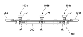
도 2는 제1 실시형태에 따른 프로브 카드 지지장치의 측면도이다.
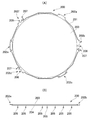
도 3은 제1 실시형태에 따른 프로브 카드의 구성을 나타낸 구성도이다.
도 4는 제1 실시형태에 따른 카드 하면 지지부의 구성을 나타낸 구성도이다.
도 5는 제1 실시형태에 따른 카드 상면 지지부의 구성을 나타낸 구성도이다.
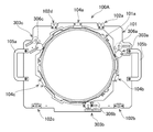
도 6은 제2 실시형태에 따른 프로브 카드 지지장치의 평면도이다.
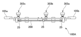
도 7은 제2 실시형태에 따른 프로브 카드 지지장치의 측면도이다.
101a: 개구부 102(102a∼102c): 위치결정 블록부
103(103a∼103c) 및 303(303a∼303c): 카드 하면(下面) 지지부
21: 손잡이부 22: 제1 받음부
23: 부세(付勢)부재 24: 제2 받음부
25: L자 부재 251: 카드 지지부
252: 기부(基部)
104(104a∼104c): 카드 상면(上面) 지지부
31: 상면(上面) 지지부 311: 아랫면(下面)
32: 단면(端面) 지지부 321: 단차(段差)부
105a 및 105b: 손잡이부재 306a∼306c: 가이드부
Claims (5)
- 판상의 프레임부의 아랫면 쪽에 프로브 카드를 지지하는 프로브 카드 지지장치로서,
상기 프레임부는, 판상부재의 중앙부에 상기 프로브 카드와 동일한 크기의 개구부를 갖고 있고,
상기 프레임부에서의 상기 개구부의 가장자리에 설치되고, 상기 프로브 카드의 가장자리의 아랫면을, 윗방향으로 힘을 가하면서 지지하는 복수의 카드 하면(下面) 지지부; 및
상기 프레임부에서의 상기 개구부의 가장자리의 아랫면에 설치되고, 상기 복수의 카드 하면 지지부에 의해 지지되는 상기 프로브 카드의 가장자리의 윗면을 지지하는 복수의 카드 상면(上面) 지지부;
를 포함하고,
상기 각 카드 하면 지지부가,
상기 프레임부의 아랫면에서 윗면을 향해 설치되는 기부와, 상기 프레임부의 아랫면 쪽에 있는 하면 지지부를 갖는 L자 부재;
상기 L자 부재의 상기 기부의 선단부와 연결하는 손잡이부; 및
상기 손잡이부와 상기 프레임부의 윗면 사이에 설치되고, 상기 프레임부의 아랫면에 대하여 상기 L자 부재의 상기 하면 지지부를 윗방향으로 힘을 가하는 부세(付勢)부재;
를 포함하는 것을 특징으로 하는 프로브 카드 지지장치.
- 제1항에 있어서, 상기 각 카드 하면 지지부의 상기 손잡이부가 회전 가능한 것이고,
상기 손잡이부의 회전에 의해, 상기 손잡이부와 연결된 상기 L자 부재의 상기 하면 지지부가, 상기 프레임부의 상기 개구부 쪽으로 돌출하는 것을 특징으로 하는 프로브 카드 지지장치.
- 제1항에 있어서, 상기 각 카드 하면 지지부의 상기 손잡이부가 상기 프레임부의 상기 개구부 쪽으로 슬라이드 가능한 것이고,
상기 손잡이부의 슬라이드에 의해, 상기 손잡이부와 연결된 상기 L자 부재의 상기 하면 지지부가, 상기 프레임부의 상기 개구부 쪽으로 돌출하는 것을 특징으로 하는 프로브 카드 지지장치.
- 제1항 내지 제3항의 어느 한 항에 있어서, 상기 각 카드 상면 지지부가, 상기 프로브 카드의 가장자리의 윗면을 지지하는 상면 지지부와, 상기 프로브 카드의 가장자리의 단면을 지지하는 단차부를 갖는 것을 특징으로 하는 프로브 카드 지지장치.
- 제1항에 있어서, 상기 복수의 카드 하면 지지부가, 상기 프레임부에서의 상기 개구부의 가장자리의 주방향으로 등간격으로 설치되고,
상기 복수의 카드 상면 지지부가, 상기 프레임부에서의 상기 개구부의 가장자리의 주방향으로 등간격으로, 그리고 상기 각 카드 하면 지지부와 마주보는 위치에 설치되어 있는 것을 특징으로 하는 프로브 카드 지지장치.
Applications Claiming Priority (2)
| Application Number | Priority Date | Filing Date | Title |
|---|---|---|---|
| JPJP-P-2018-183116 | 2018-09-28 | ||
| JP2018183116A JP7138004B2 (ja) | 2018-09-28 | 2018-09-28 | プローブカード保持具 |
Publications (2)
| Publication Number | Publication Date |
|---|---|
| KR20200036744A true KR20200036744A (ko) | 2020-04-07 |
| KR102129849B1 KR102129849B1 (ko) | 2020-08-05 |
Family
ID=69947849
Family Applications (1)
| Application Number | Title | Priority Date | Filing Date |
|---|---|---|---|
| KR1020190111533A Active KR102129849B1 (ko) | 2018-09-28 | 2019-09-09 | 프로브 카드 지지장치 |
Country Status (7)
| Country | Link |
|---|---|
| US (1) | US10989739B2 (ko) |
| JP (1) | JP7138004B2 (ko) |
| KR (1) | KR102129849B1 (ko) |
| CN (1) | CN110967620B (ko) |
| MY (1) | MY197465A (ko) |
| SG (1) | SG10201908362UA (ko) |
| TW (1) | TWI729471B (ko) |
Cited By (1)
| Publication number | Priority date | Publication date | Assignee | Title |
|---|---|---|---|---|
| KR102520852B1 (ko) * | 2022-10-14 | 2023-04-13 | 주식회사 유니밴스 | 프로브카드용 탑 보강판 |
Families Citing this family (2)
| Publication number | Priority date | Publication date | Assignee | Title |
|---|---|---|---|---|
| JP7416533B2 (ja) * | 2019-12-03 | 2024-01-17 | 株式会社協同 | プローブカード収納ケース、及びプローブカード収納ケースの下側ケース部の製造方法 |
| TWI870194B (zh) * | 2024-01-04 | 2025-01-11 | 京元電子股份有限公司 | 探針卡自動倉儲系統 |
Citations (13)
| Publication number | Priority date | Publication date | Assignee | Title |
|---|---|---|---|---|
| JPH029145A (ja) * | 1988-06-27 | 1990-01-12 | Tokyo Electron Ltd | プローブ装置 |
| JPH0794561A (ja) * | 1993-09-24 | 1995-04-07 | Tokyo Electron Ltd | プローブ装置 |
| JPH0883825A (ja) * | 1994-09-09 | 1996-03-26 | Tokyo Electron Ltd | プローブ装置 |
| JPH0943276A (ja) * | 1995-05-23 | 1997-02-14 | Tokyo Electron Ltd | プローブ装置に用いられるプローブカードデバイス |
| JPH10223708A (ja) * | 1997-02-04 | 1998-08-21 | Hewlett Packard Co <Hp> | 従順なウェハプローバ結合アダプタ |
| KR20010058701A (ko) * | 1999-12-30 | 2001-07-06 | 서성원 | 반도체 웨이퍼 테스트용 링 캐리어 장치 |
| JP2002022767A (ja) * | 2000-05-31 | 2002-01-23 | Advantest Corp | プローブコンタクトシステムの平面調整機構 |
| JP2005265658A (ja) * | 2004-03-19 | 2005-09-29 | Tokyo Electron Ltd | 複数種のテスタに対応可能なプローブ装置 |
| KR20080008271A (ko) * | 2006-07-19 | 2008-01-23 | 동경 엘렉트론 주식회사 | 프로브 카드의 고정 기구, 프로브 카드의 고정 방법 및프로브 장치 |
| JP2010122201A (ja) * | 2008-02-15 | 2010-06-03 | Sharp Corp | 半導体機能試験電気接続装置 |
| JP2011064659A (ja) * | 2009-09-21 | 2011-03-31 | Tokyo Electron Ltd | プローブカードのクランプ機構及び検査装置 |
| JP2013084685A (ja) * | 2011-10-06 | 2013-05-09 | Micronics Japan Co Ltd | プローブカードのハンドリング機構 |
| JP2014103358A (ja) | 2012-11-22 | 2014-06-05 | Tokyo Electron Ltd | プローブカードケース及びプローブカードの搬送方法 |
Family Cites Families (19)
| Publication number | Priority date | Publication date | Assignee | Title |
|---|---|---|---|---|
| JPS63293935A (ja) * | 1987-05-27 | 1988-11-30 | Hitachi Ltd | プロ−ブ検査装置 |
| JPH01161173A (ja) * | 1987-12-16 | 1989-06-23 | Tokyo Electron Ltd | プローブ装置のプローブカード自動交換方法 |
| US5695068A (en) * | 1994-09-09 | 1997-12-09 | Digital Equipment Corporation | Probe card shipping and handling system |
| JP4022335B2 (ja) * | 1999-04-15 | 2007-12-19 | 株式会社日本マイクロニクス | プローブカードの検査装置 |
| DE10039336C2 (de) * | 2000-08-04 | 2003-12-11 | Infineon Technologies Ag | Verfahren zum Testen von Halbleiterschaltungen und Testvorrichtung zur Durchführung des Verfahrens |
| JP2003324132A (ja) | 2002-04-30 | 2003-11-14 | Japan Electronic Materials Corp | テスト用基板 |
| JP4548817B2 (ja) * | 2002-10-18 | 2010-09-22 | 東京エレクトロン株式会社 | プローブ装置 |
| JP2005251813A (ja) | 2004-03-02 | 2005-09-15 | Matsushita Electric Ind Co Ltd | ウエハレベルバーンインアライメント装置およびウエハレベルバーンインアライメント方法 |
| JP4625387B2 (ja) * | 2005-09-16 | 2011-02-02 | 東京エレクトロン株式会社 | プローブカードのクランプ機構及びプローブ装置 |
| US7598727B1 (en) * | 2006-09-12 | 2009-10-06 | Xilinx, Inc. | Probe card head protection device for wafer sort set up |
| JP5190195B2 (ja) * | 2006-11-29 | 2013-04-24 | 株式会社日本マイクロニクス | 電気的接続装置 |
| JP2008216060A (ja) * | 2007-03-05 | 2008-09-18 | Micronics Japan Co Ltd | 電気的接続装置 |
| JP5134864B2 (ja) * | 2007-05-30 | 2013-01-30 | 株式会社日本マイクロニクス | 半導体検査装置 |
| US7960989B2 (en) * | 2008-12-03 | 2011-06-14 | Formfactor, Inc. | Mechanical decoupling of a probe card assembly to improve thermal response |
| TWI604198B (zh) * | 2016-06-22 | 2017-11-01 | 思達科技股份有限公司 | 測試裝置、夾持組件及探針卡載具 |
| CN206817146U (zh) * | 2017-06-26 | 2017-12-29 | 卢丽花 | 一种纺织机械防夹结构 |
| CN207116348U (zh) * | 2017-08-23 | 2018-03-16 | 四川阿尔凯电气有限公司 | 一种紧急分闸装置 |
| CN207740524U (zh) * | 2018-01-04 | 2018-08-17 | 田军璠 | 一种井口采油树阀门防护装置 |
| CN207889402U (zh) * | 2018-02-26 | 2018-09-21 | 李言哲 | 一种金融票据夹持板 |
-
2018
- 2018-09-28 JP JP2018183116A patent/JP7138004B2/ja active Active
-
2019
- 2019-08-26 TW TW108130403A patent/TWI729471B/zh active
- 2019-09-09 US US16/564,293 patent/US10989739B2/en active Active
- 2019-09-09 KR KR1020190111533A patent/KR102129849B1/ko active Active
- 2019-09-10 SG SG10201908362UA patent/SG10201908362UA/en unknown
- 2019-09-17 MY MYPI2019005348A patent/MY197465A/en unknown
- 2019-09-27 CN CN201910922675.4A patent/CN110967620B/zh active Active
Patent Citations (14)
| Publication number | Priority date | Publication date | Assignee | Title |
|---|---|---|---|---|
| JPH029145A (ja) * | 1988-06-27 | 1990-01-12 | Tokyo Electron Ltd | プローブ装置 |
| JPH0794561A (ja) * | 1993-09-24 | 1995-04-07 | Tokyo Electron Ltd | プローブ装置 |
| JPH0883825A (ja) * | 1994-09-09 | 1996-03-26 | Tokyo Electron Ltd | プローブ装置 |
| JPH0943276A (ja) * | 1995-05-23 | 1997-02-14 | Tokyo Electron Ltd | プローブ装置に用いられるプローブカードデバイス |
| JPH10223708A (ja) * | 1997-02-04 | 1998-08-21 | Hewlett Packard Co <Hp> | 従順なウェハプローバ結合アダプタ |
| KR20010058701A (ko) * | 1999-12-30 | 2001-07-06 | 서성원 | 반도체 웨이퍼 테스트용 링 캐리어 장치 |
| JP2002022767A (ja) * | 2000-05-31 | 2002-01-23 | Advantest Corp | プローブコンタクトシステムの平面調整機構 |
| JP2005265658A (ja) * | 2004-03-19 | 2005-09-29 | Tokyo Electron Ltd | 複数種のテスタに対応可能なプローブ装置 |
| KR20080008271A (ko) * | 2006-07-19 | 2008-01-23 | 동경 엘렉트론 주식회사 | 프로브 카드의 고정 기구, 프로브 카드의 고정 방법 및프로브 장치 |
| JP2010122201A (ja) * | 2008-02-15 | 2010-06-03 | Sharp Corp | 半導体機能試験電気接続装置 |
| JP2011064659A (ja) * | 2009-09-21 | 2011-03-31 | Tokyo Electron Ltd | プローブカードのクランプ機構及び検査装置 |
| JP2013084685A (ja) * | 2011-10-06 | 2013-05-09 | Micronics Japan Co Ltd | プローブカードのハンドリング機構 |
| JP2014103358A (ja) | 2012-11-22 | 2014-06-05 | Tokyo Electron Ltd | プローブカードケース及びプローブカードの搬送方法 |
| KR20150090056A (ko) * | 2012-11-22 | 2015-08-05 | 도쿄엘렉트론가부시키가이샤 | 프로브 카드 케이스 및 프로브 카드의 반송 방법 |
Cited By (1)
| Publication number | Priority date | Publication date | Assignee | Title |
|---|---|---|---|---|
| KR102520852B1 (ko) * | 2022-10-14 | 2023-04-13 | 주식회사 유니밴스 | 프로브카드용 탑 보강판 |
Also Published As
| Publication number | Publication date |
|---|---|
| CN110967620B (zh) | 2022-07-22 |
| US20200103442A1 (en) | 2020-04-02 |
| JP7138004B2 (ja) | 2022-09-15 |
| KR102129849B1 (ko) | 2020-08-05 |
| MY197465A (en) | 2023-06-19 |
| CN110967620A (zh) | 2020-04-07 |
| US10989739B2 (en) | 2021-04-27 |
| SG10201908362UA (en) | 2020-04-29 |
| TWI729471B (zh) | 2021-06-01 |
| TW202035999A (zh) | 2020-10-01 |
| JP2020053609A (ja) | 2020-04-02 |
Similar Documents
| Publication | Publication Date | Title |
|---|---|---|
| KR102129849B1 (ko) | 프로브 카드 지지장치 | |
| US6686753B1 (en) | Prober and apparatus for semiconductor chip analysis | |
| KR101887071B1 (ko) | 검사장치의 슬라이더 조작기구 | |
| KR101570215B1 (ko) | 전자 디바이스의 검사장치 | |
| CN104764986A (zh) | 基板检查装置和探针卡输送方法 | |
| US9453875B2 (en) | Multi-stage circuit board test | |
| CN104813458A (zh) | 探针卡盒和探针卡输送方法 | |
| JPWO2006097973A1 (ja) | Icキャリア,icソケット及びicデバイスの試験方法 | |
| KR101077940B1 (ko) | 반도체 패키지 인서트 장치 | |
| KR102358771B1 (ko) | Ssd 테스트 기구 및 이를 적용한 테스트 장치 | |
| CN101388517B (zh) | 测试插座 | |
| CN108352666B (zh) | 电气部件用插座 | |
| JP2016197689A (ja) | 半導体試験治具、半導体装置の試験方法 | |
| TWM514004U (zh) | 積體電路的檢測裝置及檢測設備 | |
| KR20220131890A (ko) | 웨이퍼 반송 유닛 및 웨이퍼 반송 방법 | |
| KR20160044737A (ko) | 전자 부품을 수납하기 위한 인서트 조립체 | |
| CN106970313B (zh) | 电子部件输送装置以及电子部件检查装置 | |
| KR20190135153A (ko) | 소켓 보드 조립체 | |
| JP6877260B2 (ja) | 検査用治具 | |
| KR20180090647A (ko) | 디스플레이 패널용 트레이 | |
| JP2025024953A (ja) | ソケット及び検査用ソケット | |
| KR101627869B1 (ko) | 하이픽스 보드 검사 장치 | |
| JP6593071B2 (ja) | 電子部品搬送装置および電子部品検査装置 | |
| JP2017067593A (ja) | 電子部品搬送装置および電子部品検査装置 | |
| JP2019082362A (ja) | 基板検査装置 |
Legal Events
| Date | Code | Title | Description |
|---|---|---|---|
| PA0109 | Patent application |
Patent event code: PA01091R01D Comment text: Patent Application Patent event date: 20190909 |
|
| PA0201 | Request for examination | ||
| PG1501 | Laying open of application | ||
| E701 | Decision to grant or registration of patent right | ||
| PE0701 | Decision of registration |
Patent event code: PE07011S01D Comment text: Decision to Grant Registration Patent event date: 20200624 |
|
| GRNT | Written decision to grant | ||
| PR0701 | Registration of establishment |
Comment text: Registration of Establishment Patent event date: 20200629 Patent event code: PR07011E01D |
|
| PR1002 | Payment of registration fee |
Payment date: 20200630 End annual number: 3 Start annual number: 1 |
|
| PG1601 | Publication of registration |