KR20200037244A - 촬상 소자 및 촬상 장치 - Google Patents
촬상 소자 및 촬상 장치 Download PDFInfo
- Publication number
- KR20200037244A KR20200037244A KR1020207003422A KR20207003422A KR20200037244A KR 20200037244 A KR20200037244 A KR 20200037244A KR 1020207003422 A KR1020207003422 A KR 1020207003422A KR 20207003422 A KR20207003422 A KR 20207003422A KR 20200037244 A KR20200037244 A KR 20200037244A
- Authority
- KR
- South Korea
- Prior art keywords
- pixel
- phase difference
- conversion efficiency
- light
- photoelectric conversion
- Prior art date
- Legal status (The legal status is an assumption and is not a legal conclusion. Google has not performed a legal analysis and makes no representation as to the accuracy of the status listed.)
- Ceased
Links
- 238000003384 imaging method Methods 0.000 title claims abstract description 141
- 238000006243 chemical reaction Methods 0.000 claims abstract description 138
- 238000001514 detection method Methods 0.000 claims abstract description 19
- 238000009792 diffusion process Methods 0.000 claims description 30
- 238000007667 floating Methods 0.000 claims description 30
- 238000000034 method Methods 0.000 claims description 17
- 238000005516 engineering process Methods 0.000 abstract description 11
- 238000012545 processing Methods 0.000 description 45
- 210000003128 head Anatomy 0.000 description 38
- 238000004891 communication Methods 0.000 description 28
- 230000006870 function Effects 0.000 description 24
- 230000003287 optical effect Effects 0.000 description 22
- 238000010586 diagram Methods 0.000 description 14
- 238000002674 endoscopic surgery Methods 0.000 description 12
- 239000004065 semiconductor Substances 0.000 description 11
- 239000010410 layer Substances 0.000 description 10
- 238000007789 sealing Methods 0.000 description 10
- 238000001356 surgical procedure Methods 0.000 description 10
- 239000000758 substrate Substances 0.000 description 9
- 230000005540 biological transmission Effects 0.000 description 8
- 230000000694 effects Effects 0.000 description 7
- 238000010336 energy treatment Methods 0.000 description 7
- 238000012546 transfer Methods 0.000 description 6
- CNQCVBJFEGMYDW-UHFFFAOYSA-N lawrencium atom Chemical compound [Lr] CNQCVBJFEGMYDW-UHFFFAOYSA-N 0.000 description 5
- 238000013139 quantization Methods 0.000 description 5
- 230000005284 excitation Effects 0.000 description 4
- 210000004204 blood vessel Anatomy 0.000 description 3
- 238000005286 illumination Methods 0.000 description 3
- 230000001678 irradiating effect Effects 0.000 description 3
- 230000035945 sensitivity Effects 0.000 description 3
- XUIMIQQOPSSXEZ-UHFFFAOYSA-N Silicon Chemical compound [Si] XUIMIQQOPSSXEZ-UHFFFAOYSA-N 0.000 description 2
- 210000003815 abdominal wall Anatomy 0.000 description 2
- 230000002411 adverse Effects 0.000 description 2
- 230000008901 benefit Effects 0.000 description 2
- 230000008859 change Effects 0.000 description 2
- 239000003153 chemical reaction reagent Substances 0.000 description 2
- 230000000295 complement effect Effects 0.000 description 2
- 238000010276 construction Methods 0.000 description 2
- 230000002950 deficient Effects 0.000 description 2
- 230000006866 deterioration Effects 0.000 description 2
- 238000011161 development Methods 0.000 description 2
- MOFVSTNWEDAEEK-UHFFFAOYSA-M indocyanine green Chemical compound [Na+].[O-]S(=O)(=O)CCCCN1C2=CC=C3C=CC=CC3=C2C(C)(C)C1=CC=CC=CC=CC1=[N+](CCCCS([O-])(=O)=O)C2=CC=C(C=CC=C3)C3=C2C1(C)C MOFVSTNWEDAEEK-UHFFFAOYSA-M 0.000 description 2
- 229960004657 indocyanine green Drugs 0.000 description 2
- 229910044991 metal oxide Inorganic materials 0.000 description 2
- 150000004706 metal oxides Chemical class 0.000 description 2
- 238000012544 monitoring process Methods 0.000 description 2
- 229910052710 silicon Inorganic materials 0.000 description 2
- 239000010703 silicon Substances 0.000 description 2
- 230000009471 action Effects 0.000 description 1
- 238000002583 angiography Methods 0.000 description 1
- 230000000740 bleeding effect Effects 0.000 description 1
- 230000000903 blocking effect Effects 0.000 description 1
- 239000003990 capacitor Substances 0.000 description 1
- 239000002131 composite material Substances 0.000 description 1
- 238000012937 correction Methods 0.000 description 1
- 239000002537 cosmetic Substances 0.000 description 1
- 238000003745 diagnosis Methods 0.000 description 1
- 230000036541 health Effects 0.000 description 1
- 238000007689 inspection Methods 0.000 description 1
- 230000031700 light absorption Effects 0.000 description 1
- 238000004519 manufacturing process Methods 0.000 description 1
- 230000007246 mechanism Effects 0.000 description 1
- 239000003595 mist Substances 0.000 description 1
- 239000000203 mixture Substances 0.000 description 1
- 229910021421 monocrystalline silicon Inorganic materials 0.000 description 1
- 239000013307 optical fiber Substances 0.000 description 1
- 230000001151 other effect Effects 0.000 description 1
- 230000005622 photoelectricity Effects 0.000 description 1
- 238000007639 printing Methods 0.000 description 1
- 210000001747 pupil Anatomy 0.000 description 1
- 230000009467 reduction Effects 0.000 description 1
- 230000004044 response Effects 0.000 description 1
- 229920006395 saturated elastomer Polymers 0.000 description 1
- 210000004761 scalp Anatomy 0.000 description 1
- 238000000926 separation method Methods 0.000 description 1
- 230000001954 sterilising effect Effects 0.000 description 1
- 238000004659 sterilization and disinfection Methods 0.000 description 1
- 239000002344 surface layer Substances 0.000 description 1
Images






Classifications
-
- H—ELECTRICITY
- H04—ELECTRIC COMMUNICATION TECHNIQUE
- H04N—PICTORIAL COMMUNICATION, e.g. TELEVISION
- H04N9/00—Details of colour television systems
- H04N9/01—Circuitry for demodulating colour component signals modulated spatially by colour striped filters by phase separation
-
- H04N5/36961—
-
- G—PHYSICS
- G02—OPTICS
- G02B—OPTICAL ELEMENTS, SYSTEMS OR APPARATUS
- G02B7/00—Mountings, adjusting means, or light-tight connections, for optical elements
- G02B7/28—Systems for automatic generation of focusing signals
- G02B7/34—Systems for automatic generation of focusing signals using different areas in a pupil plane
-
- G—PHYSICS
- G03—PHOTOGRAPHY; CINEMATOGRAPHY; ANALOGOUS TECHNIQUES USING WAVES OTHER THAN OPTICAL WAVES; ELECTROGRAPHY; HOLOGRAPHY
- G03B—APPARATUS OR ARRANGEMENTS FOR TAKING PHOTOGRAPHS OR FOR PROJECTING OR VIEWING THEM; APPARATUS OR ARRANGEMENTS EMPLOYING ANALOGOUS TECHNIQUES USING WAVES OTHER THAN OPTICAL WAVES; ACCESSORIES THEREFOR
- G03B13/00—Viewfinders; Focusing aids for cameras; Means for focusing for cameras; Autofocus systems for cameras
- G03B13/32—Means for focusing
- G03B13/34—Power focusing
- G03B13/36—Autofocus systems
-
- H01L27/14621—
-
- H01L27/14627—
-
- H—ELECTRICITY
- H04—ELECTRIC COMMUNICATION TECHNIQUE
- H04N—PICTORIAL COMMUNICATION, e.g. TELEVISION
- H04N23/00—Cameras or camera modules comprising electronic image sensors; Control thereof
- H04N23/10—Cameras or camera modules comprising electronic image sensors; Control thereof for generating image signals from different wavelengths
- H04N23/12—Cameras or camera modules comprising electronic image sensors; Control thereof for generating image signals from different wavelengths with one sensor only
-
- H—ELECTRICITY
- H04—ELECTRIC COMMUNICATION TECHNIQUE
- H04N—PICTORIAL COMMUNICATION, e.g. TELEVISION
- H04N23/00—Cameras or camera modules comprising electronic image sensors; Control thereof
- H04N23/50—Constructional details
- H04N23/54—Mounting of pick-up tubes, electronic image sensors, deviation or focusing coils
-
- H—ELECTRICITY
- H04—ELECTRIC COMMUNICATION TECHNIQUE
- H04N—PICTORIAL COMMUNICATION, e.g. TELEVISION
- H04N25/00—Circuitry of solid-state image sensors [SSIS]; Control thereof
- H04N25/10—Circuitry of solid-state image sensors [SSIS]; Control thereof for transforming different wavelengths into image signals
- H04N25/11—Arrangement of colour filter arrays [CFA]; Filter mosaics
-
- H—ELECTRICITY
- H04—ELECTRIC COMMUNICATION TECHNIQUE
- H04N—PICTORIAL COMMUNICATION, e.g. TELEVISION
- H04N25/00—Circuitry of solid-state image sensors [SSIS]; Control thereof
- H04N25/10—Circuitry of solid-state image sensors [SSIS]; Control thereof for transforming different wavelengths into image signals
- H04N25/11—Arrangement of colour filter arrays [CFA]; Filter mosaics
- H04N25/13—Arrangement of colour filter arrays [CFA]; Filter mosaics characterised by the spectral characteristics of the filter elements
- H04N25/134—Arrangement of colour filter arrays [CFA]; Filter mosaics characterised by the spectral characteristics of the filter elements based on three different wavelength filter elements
-
- H—ELECTRICITY
- H04—ELECTRIC COMMUNICATION TECHNIQUE
- H04N—PICTORIAL COMMUNICATION, e.g. TELEVISION
- H04N25/00—Circuitry of solid-state image sensors [SSIS]; Control thereof
- H04N25/40—Extracting pixel data from image sensors by controlling scanning circuits, e.g. by modifying the number of pixels sampled or to be sampled
- H04N25/46—Extracting pixel data from image sensors by controlling scanning circuits, e.g. by modifying the number of pixels sampled or to be sampled by combining or binning pixels
-
- H—ELECTRICITY
- H04—ELECTRIC COMMUNICATION TECHNIQUE
- H04N—PICTORIAL COMMUNICATION, e.g. TELEVISION
- H04N25/00—Circuitry of solid-state image sensors [SSIS]; Control thereof
- H04N25/70—SSIS architectures; Circuits associated therewith
- H04N25/703—SSIS architectures incorporating pixels for producing signals other than image signals
- H04N25/704—Pixels specially adapted for focusing, e.g. phase difference pixel sets
-
- H—ELECTRICITY
- H04—ELECTRIC COMMUNICATION TECHNIQUE
- H04N—PICTORIAL COMMUNICATION, e.g. TELEVISION
- H04N25/00—Circuitry of solid-state image sensors [SSIS]; Control thereof
- H04N25/70—SSIS architectures; Circuits associated therewith
- H04N25/76—Addressed sensors, e.g. MOS or CMOS sensors
-
- H—ELECTRICITY
- H04—ELECTRIC COMMUNICATION TECHNIQUE
- H04N—PICTORIAL COMMUNICATION, e.g. TELEVISION
- H04N25/00—Circuitry of solid-state image sensors [SSIS]; Control thereof
- H04N25/70—SSIS architectures; Circuits associated therewith
- H04N25/76—Addressed sensors, e.g. MOS or CMOS sensors
- H04N25/77—Pixel circuitry, e.g. memories, A/D converters, pixel amplifiers, shared circuits or shared components
- H04N25/778—Pixel circuitry, e.g. memories, A/D converters, pixel amplifiers, shared circuits or shared components comprising amplifiers shared between a plurality of pixels, i.e. at least one part of the amplifier must be on the sensor array itself
-
- H04N5/2253—
-
- H04N5/374—
-
- H04N9/0455—
-
- H—ELECTRICITY
- H10—SEMICONDUCTOR DEVICES; ELECTRIC SOLID-STATE DEVICES NOT OTHERWISE PROVIDED FOR
- H10F—INORGANIC SEMICONDUCTOR DEVICES SENSITIVE TO INFRARED RADIATION, LIGHT, ELECTROMAGNETIC RADIATION OF SHORTER WAVELENGTH OR CORPUSCULAR RADIATION
- H10F39/00—Integrated devices, or assemblies of multiple devices, comprising at least one element covered by group H10F30/00, e.g. radiation detectors comprising photodiode arrays
- H10F39/10—Integrated devices
- H10F39/12—Image sensors
- H10F39/18—Complementary metal-oxide-semiconductor [CMOS] image sensors; Photodiode array image sensors
-
- H—ELECTRICITY
- H10—SEMICONDUCTOR DEVICES; ELECTRIC SOLID-STATE DEVICES NOT OTHERWISE PROVIDED FOR
- H10F—INORGANIC SEMICONDUCTOR DEVICES SENSITIVE TO INFRARED RADIATION, LIGHT, ELECTROMAGNETIC RADIATION OF SHORTER WAVELENGTH OR CORPUSCULAR RADIATION
- H10F39/00—Integrated devices, or assemblies of multiple devices, comprising at least one element covered by group H10F30/00, e.g. radiation detectors comprising photodiode arrays
- H10F39/80—Constructional details of image sensors
- H10F39/802—Geometry or disposition of elements in pixels, e.g. address-lines or gate electrodes
-
- H—ELECTRICITY
- H10—SEMICONDUCTOR DEVICES; ELECTRIC SOLID-STATE DEVICES NOT OTHERWISE PROVIDED FOR
- H10F—INORGANIC SEMICONDUCTOR DEVICES SENSITIVE TO INFRARED RADIATION, LIGHT, ELECTROMAGNETIC RADIATION OF SHORTER WAVELENGTH OR CORPUSCULAR RADIATION
- H10F39/00—Integrated devices, or assemblies of multiple devices, comprising at least one element covered by group H10F30/00, e.g. radiation detectors comprising photodiode arrays
- H10F39/80—Constructional details of image sensors
- H10F39/803—Pixels having integrated switching, control, storage or amplification elements
-
- H—ELECTRICITY
- H10—SEMICONDUCTOR DEVICES; ELECTRIC SOLID-STATE DEVICES NOT OTHERWISE PROVIDED FOR
- H10F—INORGANIC SEMICONDUCTOR DEVICES SENSITIVE TO INFRARED RADIATION, LIGHT, ELECTROMAGNETIC RADIATION OF SHORTER WAVELENGTH OR CORPUSCULAR RADIATION
- H10F39/00—Integrated devices, or assemblies of multiple devices, comprising at least one element covered by group H10F30/00, e.g. radiation detectors comprising photodiode arrays
- H10F39/80—Constructional details of image sensors
- H10F39/805—Coatings
- H10F39/8053—Colour filters
-
- H—ELECTRICITY
- H10—SEMICONDUCTOR DEVICES; ELECTRIC SOLID-STATE DEVICES NOT OTHERWISE PROVIDED FOR
- H10F—INORGANIC SEMICONDUCTOR DEVICES SENSITIVE TO INFRARED RADIATION, LIGHT, ELECTROMAGNETIC RADIATION OF SHORTER WAVELENGTH OR CORPUSCULAR RADIATION
- H10F39/00—Integrated devices, or assemblies of multiple devices, comprising at least one element covered by group H10F30/00, e.g. radiation detectors comprising photodiode arrays
- H10F39/80—Constructional details of image sensors
- H10F39/805—Coatings
- H10F39/8057—Optical shielding
-
- H—ELECTRICITY
- H10—SEMICONDUCTOR DEVICES; ELECTRIC SOLID-STATE DEVICES NOT OTHERWISE PROVIDED FOR
- H10F—INORGANIC SEMICONDUCTOR DEVICES SENSITIVE TO INFRARED RADIATION, LIGHT, ELECTROMAGNETIC RADIATION OF SHORTER WAVELENGTH OR CORPUSCULAR RADIATION
- H10F39/00—Integrated devices, or assemblies of multiple devices, comprising at least one element covered by group H10F30/00, e.g. radiation detectors comprising photodiode arrays
- H10F39/80—Constructional details of image sensors
- H10F39/806—Optical elements or arrangements associated with the image sensors
- H10F39/8063—Microlenses
Landscapes
- Signal Processing (AREA)
- Engineering & Computer Science (AREA)
- Multimedia (AREA)
- Physics & Mathematics (AREA)
- General Physics & Mathematics (AREA)
- Optics & Photonics (AREA)
- Spectroscopy & Molecular Physics (AREA)
- Studio Devices (AREA)
- Focusing (AREA)
- Solid State Image Pick-Up Elements (AREA)
- Transforming Light Signals Into Electric Signals (AREA)
- Color Television Image Signal Generators (AREA)
- Blocking Light For Cameras (AREA)
- Automatic Focus Adjustment (AREA)
Abstract
Description
[도 2] 통상 화소 및 위상차 화소의 제1 배치 패턴을 나타내는 도면이다.
[도 3] 위상차 화소의 제1 내지 제3 구성예를 나타내는 도면이다.
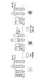
[도 4] 위상차 화소의 변환효율에 대해서 설명하는 도면이다.
[도 5] 통상 화소 및 위상차 화소의 제2 배치 패턴을 나타내는 도면이다.
[도 6] 위상차 화소의 제4 및 제5 구성예를 나타내는 도면이다.
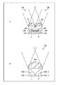
[도 7] 대형의 마이크로 렌즈를 채용하는 구성의 장점에 대해서 설명하는 도면이다.
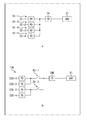
[도8] 4화소가산이 행해지는 구조에서의 배선 구성의 일례를 나타내는 도면이다.
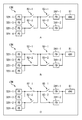
[도9] 통상 화소 모드 및 위상차 화소 모드를 전환할 수 있는 위상차 화소의 구성예에 대해서 설명하는 도면이다.
[도 10] 촬상 장치의 구성예를 나타내는 블록도이다.
[도 11] 이미지 센서를 사용하는 사용 예를 나타내는 도면이다.
[도 12] 수술실 시스템의 전체구성을 개략적으로 나타내는 도면이다.
[도 13] 집중 조작 패널에 있어서의 조작 화면의 표시예를 나타내는 도면이다.
[도 14] 수술실 시스템이 적용된 수술의 모습의 일례를 나타내는 도면이다.
[도 15] 도 14에 나타내는 카메라 헤드 및 CCU의 기능 구성에 일례를 나타내
는 블록도이다.
12: 통상 화소
13: 위상차 화소
21: 반도체기판
22: 평탄화층
23: 필터층
24: 온 칩 렌즈층
31: 실리콘 웨이퍼
32: PD
33: 전송 트랜지스터
34: FD부
35: 화소간 차광막
36: 위상차 차광막
37 및 38: 개구부
41: 산화막
51: 컬러 필터
52: 투명 필터
61: 마이크로 렌즈
71: 증폭 트랜지스터
72: 선택 트랜지스터
73: 수직신호선
81: AD컨버터
82: 절환 트랜지스터
Claims (18)
- 광전 변환에 의해 발생한 전하를 제1 변환효율로 전압으로 변환하여, 화상의 구축에 이용되는 화소 신호를 출력하는 제1 화소와,
광전 변환에 의해 발생한 전하를 상기 제1 변환효율보다 큰 제2 변환효율로 전압으로 변환하여, 위상차 검출에 이용되는 화소 신호를 출력하는 제2 화소를 구비하는 촬상 소자. - 제1항에 있어서,
상기 변환효율은, 상기 제1 화소가 광을 수광하는 수광 면적과, 상기 제2 화소가 광을 수광하는 수광 면적과의 비율에 따라 설정되는 촬상 소자. - 제2항에 있어서,
상기 제2 화소는, 차광성을 구비한 위상차 차광막에 의해 수광 면적의 약 절반이 차광 되어 있고,
상기 제2 변환효율이, 상기 제1 변환효율의 약2배인 촬상 소자. - 제1항에 있어서,
상기 제1 화소 및 상기 제2 화소는,
수광한 광을 광전 변환하는 광전 변환부와,
상기 광전 변환부에서 발생한 전하를 일시적으로 축적하는 부유 확산 영역과,
상기 부유 확산 영역에 축적되어 있는 전하를, 상기 부유 확산 영역의 용량에 따른 변환효율로, 상기 화소 신호를 나타내는 전압으로 변환하는 전하전압변환부를 각각 가지고 있으며,
상기 제2 화소가 가지는 상기 부유 확산 영역의 용량이, 상기 제1 화소가 가지는 상기 부유 확산 영역의 용량보다도 작아지도록 형성된 촬상 소자. - 제4항에 있어서,
상기 제2 화소가 가지는 상기 부유 확산 영역의 용량이, 상기 제1 화소가 가지는 상기 부유 확산 영역의 용량의 약 절반이 되도록 형성함으로써, 상기 제2 변환효율이, 상기 제1 변환효율의 약 2배로 설정되는 촬상 소자. - 제1항에 있어서,
상기 제2 화소는, 4개의 광전 변환부가 세로×가로가 2Х2가 되는 배치로 구성되어 있고,
이들 4개의 상기 광전 변환부가 배치되는 영역에 따른 사이즈의 마이크로 렌즈를 더 구비하는 촬상 소자. - 제6항에 있어서,
세로×가로가 2Х2로 배치된 4개의 상기 제1 화소마다, 적색, 녹색 및 청색의 광을 수광하도록 컬러 필터가 배치되어 있는 촬상 소자. - 제1항에 있어서,
상기 제2 화소는, 상기 화상의 구축에 이용되는 화소 신호를 출력하는 제1 모드와, 상기 위상차 검출에 이용되는 화소 신호를 출력하는 제2 모드를 절환할 수 있고, 상기 제1 모드일 때에는 상기 제1 변환효율로 전하를 전압으로 변환하고, 상기 제2 모드일 때에는 상기 제2의 변환효율로 전하를 전압으로 변환하는 촬상 소자. - 제8항에 있어서,
상기 제2 화소는, 2개 이상의 광전 변환부를 가지도록 구성되어 있고, 상기 제1 모드의 경우, 모든 상기 광전 변환부의 전하를 전압으로 변환하고, 상기 제2 모드의 경우, 일부의 상기 광전 변환부의 전하를 전압으로 하는 촬상 소자. - 광전 변환에 의해 발생한 전하를 제1 변환효율로 전압으로 변환하여, 화상의 구축에 이용되는 화소 신호를 출력하는 제1 화소와,
광전 변환에 의해 발생한 전하를 상기 제1 변환효율보다 큰 제2 변환효율로 전압으로 변환하여, 위상차 검출에 이용되는 화소 신호를 출력하는 제2 화소를 가지는 촬상 소자를 구비하는 촬상 장치. - 제10항에 있어서,
상기 변환효율은, 상기 제1 화소가 광을 수광하는 수광 면적과, 상기 제2 화소가 광을 수광하는 수광 면적과의 비율에 따라 설정되는 촬상 장치. - 제11항에 있어서,
상기 제2의 화소는, 차광성을 구비한 위상차 차광막에 의해 수광 면적의 약 절반이 차광 되어 있고,
상기 제의 변환효율이, 상기 제1 변환효율의 약2배인 촬상 장치. - 제10항에 있어서,
상기 제1 화소 및 상기 제2 화소는,
수광한 광을 광전 변환하는 광전 변환부와,
상기 광전 변환부에서 발생한 전하를 일시적으로 축적하는 부유 확산 영역과,
상기 부유 확산 영역에 축적되어 있는 전하를, 상기 부유 확산 영역의 용량에 따른 변환효율로, 상기 화소 신호를 나타내는 전압으로 변환하는 전하전압변환부를 각각 가지고 있으며,
상기 제2 화소가 가지는 상기 부유 확산 영역의 용량이, 상기 제1 화소가 가지는 상기 부유 확산 영역의 용량보다도 작아지도록 형성된 촬상 장치. - 제13항에 있어서,
상기 제2 화소가 가지는 상기 부유 확산 영역의 용량이, 상기 제1 화소가 가지는 상기 부유 확산 영역의 용량의 약 절반이 되도록 형성함으로써, 상기 제2 변환효율이, 상기 제1 변환효율의 약 2배로 설정되는 촬상 장치. - 제10항에 있어서,
상기 제2 화소는, 4개의 광전 변환부가 세로×가로가 2Х2가 되는 배치로 구성되어 있고,
이들 4개의 상기 광전 변환부가 배치되는 영역에 따른 사이즈의 마이크로 렌즈를 더 구비하는 촬상 장치. - 제15항에 있어서,
세로×가로가 2Х2로 배치된 4개의 상기 제1 화소마다, 적색, 녹색 및 청색의 광을 수광하도록 컬러 필터가 배치되어 있는 촬상 장치. - 제10항에 있어서,
상기 제2 화소는, 상기 화상의 구축에 이용되는 화소 신호를 출력하는 제1 모드와, 상기 위상차 검출에 이용되는 화소 신호를 출력하는 제2 모드를 절환할 수 있고, 상기 제1 모드일 때에는 상기 제1 변환효율로 전하를 전압으로 변환하고, 상기 제2 모드일 때에는 상기 제2 변환효율로 전하를 전압으로 변환하는 촬상 장치. - 제17항에 있어서,
상기 제2 화소는, 2개 이상의 광전 변환부를 가지도록 구성되어 있고, 상기 제1 모드의 경우, 모든 상기 광전 변환부의 전하를 전압으로 변환하고, 상기 제2 모드의 경우, 일부의 상기 광전 변환부의 전하를 전압으로 하는 촬상 장치.
Applications Claiming Priority (3)
| Application Number | Priority Date | Filing Date | Title |
|---|---|---|---|
| JP2017158066 | 2017-08-18 | ||
| JPJP-P-2017-158066 | 2017-08-18 | ||
| PCT/JP2018/029181 WO2019035374A1 (ja) | 2017-08-18 | 2018-08-03 | 撮像素子および撮像装置 |
Publications (1)
| Publication Number | Publication Date |
|---|---|
| KR20200037244A true KR20200037244A (ko) | 2020-04-08 |
Family
ID=65361889
Family Applications (1)
| Application Number | Title | Priority Date | Filing Date |
|---|---|---|---|
| KR1020207003422A Ceased KR20200037244A (ko) | 2017-08-18 | 2018-08-03 | 촬상 소자 및 촬상 장치 |
Country Status (4)
| Country | Link |
|---|---|
| US (1) | US20200169704A1 (ko) |
| JP (1) | JP7230808B2 (ko) |
| KR (1) | KR20200037244A (ko) |
| WO (1) | WO2019035374A1 (ko) |
Cited By (1)
| Publication number | Priority date | Publication date | Assignee | Title |
|---|---|---|---|---|
| KR20220147448A (ko) * | 2021-04-27 | 2022-11-03 | 삼성전자주식회사 | 색분리 렌즈 어레이를 구비하는 이미지 센서 및 이를 포함하는 전자 장치 |
Families Citing this family (13)
| Publication number | Priority date | Publication date | Assignee | Title |
|---|---|---|---|---|
| JP7230807B2 (ja) * | 2017-08-09 | 2023-03-01 | ソニーグループ株式会社 | 信号処理装置、撮像装置、信号処理方法及びプログラム |
| JP7472902B2 (ja) * | 2019-03-29 | 2024-04-23 | Toppanホールディングス株式会社 | 固体撮像装置、撮像システム及び撮像方法 |
| US12231791B2 (en) | 2019-07-02 | 2025-02-18 | Sony Semiconductor Solutions Corporation | Solid-state imaging device, method for driving the same, and electronic device |
| JP7486929B2 (ja) * | 2019-08-22 | 2024-05-20 | ソニーセミコンダクタソリューションズ株式会社 | 撮像素子、測距装置 |
| JP7692840B2 (ja) * | 2019-12-17 | 2025-06-16 | ソニーセミコンダクタソリューションズ株式会社 | 撮像素子、撮像素子の駆動方法および電子機器 |
| KR102727266B1 (ko) * | 2020-02-18 | 2024-11-07 | 에스케이하이닉스 주식회사 | 이미지 센서 및 이를 포함하는 촬영 장치 |
| WO2021166672A1 (ja) * | 2020-02-20 | 2021-08-26 | ソニーセミコンダクタソリューションズ株式会社 | 撮像装置、電子機器 |
| US11284045B2 (en) * | 2020-04-22 | 2022-03-22 | OmniVision Technologies. Inc. | Image sensor with shifted color filter array pattern and bit line pairs |
| WO2021241015A1 (ja) * | 2020-05-25 | 2021-12-02 | ソニーグループ株式会社 | 撮像装置、撮像方法 |
| KR102889849B1 (ko) | 2020-11-24 | 2025-11-27 | 삼성전자주식회사 | 이미지 센서 |
| KR20230055626A (ko) * | 2021-10-19 | 2023-04-26 | 에스케이하이닉스 주식회사 | 촬영 장치 |
| JPWO2023181735A1 (ko) * | 2022-03-25 | 2023-09-28 | ||
| JP2024168191A (ja) * | 2023-05-23 | 2024-12-05 | ソニーセミコンダクタソリューションズ株式会社 | 光検出装置及び電子機器 |
Citations (1)
| Publication number | Priority date | Publication date | Assignee | Title |
|---|---|---|---|---|
| JP2015091025A (ja) | 2013-11-06 | 2015-05-11 | ソニー株式会社 | 固体撮像装置およびその駆動方法、並びに電子機器 |
Family Cites Families (4)
| Publication number | Priority date | Publication date | Assignee | Title |
|---|---|---|---|---|
| EP2690874A4 (en) * | 2011-03-24 | 2014-09-03 | Fujifilm Corp | COLOR IMAGE SENSOR, IMAGING DEVICE AND CONTROL PLAN FOR THE IMAGING APPARATUS |
| JP5744599B2 (ja) * | 2011-03-31 | 2015-07-08 | キヤノン株式会社 | 撮像素子、および撮像装置 |
| WO2015045785A1 (ja) * | 2013-09-30 | 2015-04-02 | 富士フイルム株式会社 | 画像処理装置、撮像装置、画像処理方法及び画像処理プログラム |
| CN107004685B (zh) * | 2014-12-18 | 2022-06-14 | 索尼公司 | 固体摄像器件和电子装置 |
-
2018
- 2018-08-03 KR KR1020207003422A patent/KR20200037244A/ko not_active Ceased
- 2018-08-03 JP JP2019536736A patent/JP7230808B2/ja active Active
- 2018-08-03 US US16/638,243 patent/US20200169704A1/en not_active Abandoned
- 2018-08-03 WO PCT/JP2018/029181 patent/WO2019035374A1/ja not_active Ceased
Patent Citations (1)
| Publication number | Priority date | Publication date | Assignee | Title |
|---|---|---|---|---|
| JP2015091025A (ja) | 2013-11-06 | 2015-05-11 | ソニー株式会社 | 固体撮像装置およびその駆動方法、並びに電子機器 |
Cited By (2)
| Publication number | Priority date | Publication date | Assignee | Title |
|---|---|---|---|---|
| KR20220147448A (ko) * | 2021-04-27 | 2022-11-03 | 삼성전자주식회사 | 색분리 렌즈 어레이를 구비하는 이미지 센서 및 이를 포함하는 전자 장치 |
| US12300710B2 (en) | 2021-04-27 | 2025-05-13 | Samsung Electronics Co., Ltd. | Image sensor including color separating lens array and electronic apparatus including the image sensor |
Also Published As
| Publication number | Publication date |
|---|---|
| JPWO2019035374A1 (ja) | 2020-10-08 |
| US20200169704A1 (en) | 2020-05-28 |
| WO2019035374A1 (ja) | 2019-02-21 |
| JP7230808B2 (ja) | 2023-03-01 |
Similar Documents
| Publication | Publication Date | Title |
|---|---|---|
| JP7230808B2 (ja) | 撮像素子および撮像装置 | |
| US20230124400A1 (en) | Imaging device and electronic device | |
| US12004722B2 (en) | Microscope system and medical light source apparatus | |
| JP6915615B2 (ja) | 撮像素子、撮像装置、電子機器 | |
| US11729493B2 (en) | Image capture apparatus and image capture method | |
| US11729519B2 (en) | Video signal processing apparatus, video signal processing method, and image-capturing apparatus | |
| US11503980B2 (en) | Surgical system and surgical imaging device | |
| US12355935B2 (en) | Medical imaging system, medical imaging device, and operation method | |
| WO2019198553A1 (en) | Microscope system and medical light source apparatus | |
| US20230248231A1 (en) | Medical system, information processing apparatus, and information processing method | |
| US20220217260A1 (en) | Signal processing device, imaging device, and signal processing method | |
| CN110945399B (zh) | 信号处理设备、成像设备、信号处理方法和存储器 | |
| JP2019042413A (ja) | 医療用観察装置、および医療用観察システム | |
| US11039067B2 (en) | Image pickup apparatus, video signal processing apparatus, and video signal processing method | |
| US12102296B2 (en) | Medical imaging system, medical imaging device, and operation method | |
| US10917555B2 (en) | Imaging apparatus, focus control method, and focus determination method | |
| US11979670B2 (en) | Image processing apparatus, imaging apparatus, image processing method, and program for blending plurality of image signals based on a peaking signal |
Legal Events
| Date | Code | Title | Description |
|---|---|---|---|
| PA0105 | International application |
Patent event date: 20200205 Patent event code: PA01051R01D Comment text: International Patent Application |
|
| PG1501 | Laying open of application | ||
| A201 | Request for examination | ||
| PA0201 | Request for examination |
Patent event code: PA02012R01D Patent event date: 20210616 Comment text: Request for Examination of Application |
|
| E902 | Notification of reason for refusal | ||
| PE0902 | Notice of grounds for rejection |
Comment text: Notification of reason for refusal Patent event date: 20221020 Patent event code: PE09021S01D |
|
| E601 | Decision to refuse application | ||
| PE0601 | Decision on rejection of patent |
Patent event date: 20230410 Comment text: Decision to Refuse Application Patent event code: PE06012S01D Patent event date: 20221020 Comment text: Notification of reason for refusal Patent event code: PE06011S01I |