KR20200039849A - 포토마스크 세정 프로세스들 - Google Patents
포토마스크 세정 프로세스들 Download PDFInfo
- Publication number
- KR20200039849A KR20200039849A KR1020207010352A KR20207010352A KR20200039849A KR 20200039849 A KR20200039849 A KR 20200039849A KR 1020207010352 A KR1020207010352 A KR 1020207010352A KR 20207010352 A KR20207010352 A KR 20207010352A KR 20200039849 A KR20200039849 A KR 20200039849A
- Authority
- KR
- South Korea
- Prior art keywords
- photomask
- etchant
- coupling material
- clean
- less
- Prior art date
- Legal status (The legal status is an assumption and is not a legal conclusion. Google has not performed a legal analysis and makes no representation as to the accuracy of the status listed.)
- Granted
Links
Images




Classifications
-
- G—PHYSICS
- G03—PHOTOGRAPHY; CINEMATOGRAPHY; ANALOGOUS TECHNIQUES USING WAVES OTHER THAN OPTICAL WAVES; ELECTROGRAPHY; HOLOGRAPHY
- G03F—PHOTOMECHANICAL PRODUCTION OF TEXTURED OR PATTERNED SURFACES, e.g. FOR PRINTING, FOR PROCESSING OF SEMICONDUCTOR DEVICES; MATERIALS THEREFOR; ORIGINALS THEREFOR; APPARATUS SPECIALLY ADAPTED THEREFOR
- G03F7/00—Photomechanical, e.g. photolithographic, production of textured or patterned surfaces, e.g. printing surfaces; Materials therefor, e.g. comprising photoresists; Apparatus specially adapted therefor
- G03F7/70—Microphotolithographic exposure; Apparatus therefor
- G03F7/708—Construction of apparatus, e.g. environment aspects, hygiene aspects or materials
- G03F7/70908—Hygiene, e.g. preventing apparatus pollution, mitigating effect of pollution or removing pollutants from apparatus
- G03F7/70925—Cleaning, i.e. actively freeing apparatus from pollutants, e.g. using plasma cleaning
-
- G—PHYSICS
- G03—PHOTOGRAPHY; CINEMATOGRAPHY; ANALOGOUS TECHNIQUES USING WAVES OTHER THAN OPTICAL WAVES; ELECTROGRAPHY; HOLOGRAPHY
- G03F—PHOTOMECHANICAL PRODUCTION OF TEXTURED OR PATTERNED SURFACES, e.g. FOR PRINTING, FOR PROCESSING OF SEMICONDUCTOR DEVICES; MATERIALS THEREFOR; ORIGINALS THEREFOR; APPARATUS SPECIALLY ADAPTED THEREFOR
- G03F1/00—Originals for photomechanical production of textured or patterned surfaces, e.g., masks, photo-masks, reticles; Mask blanks or pellicles therefor; Containers specially adapted therefor; Preparation thereof
- G03F1/68—Preparation processes not covered by groups G03F1/20 - G03F1/50
- G03F1/82—Auxiliary processes, e.g. cleaning or inspecting
-
- G—PHYSICS
- G03—PHOTOGRAPHY; CINEMATOGRAPHY; ANALOGOUS TECHNIQUES USING WAVES OTHER THAN OPTICAL WAVES; ELECTROGRAPHY; HOLOGRAPHY
- G03F—PHOTOMECHANICAL PRODUCTION OF TEXTURED OR PATTERNED SURFACES, e.g. FOR PRINTING, FOR PROCESSING OF SEMICONDUCTOR DEVICES; MATERIALS THEREFOR; ORIGINALS THEREFOR; APPARATUS SPECIALLY ADAPTED THEREFOR
- G03F1/00—Originals for photomechanical production of textured or patterned surfaces, e.g., masks, photo-masks, reticles; Mask blanks or pellicles therefor; Containers specially adapted therefor; Preparation thereof
- G03F1/22—Masks or mask blanks for imaging by radiation of 100nm or shorter wavelength, e.g. X-ray masks, extreme ultraviolet [EUV] masks; Preparation thereof
-
- G—PHYSICS
- G03—PHOTOGRAPHY; CINEMATOGRAPHY; ANALOGOUS TECHNIQUES USING WAVES OTHER THAN OPTICAL WAVES; ELECTROGRAPHY; HOLOGRAPHY
- G03F—PHOTOMECHANICAL PRODUCTION OF TEXTURED OR PATTERNED SURFACES, e.g. FOR PRINTING, FOR PROCESSING OF SEMICONDUCTOR DEVICES; MATERIALS THEREFOR; ORIGINALS THEREFOR; APPARATUS SPECIALLY ADAPTED THEREFOR
- G03F1/00—Originals for photomechanical production of textured or patterned surfaces, e.g., masks, photo-masks, reticles; Mask blanks or pellicles therefor; Containers specially adapted therefor; Preparation thereof
- G03F1/62—Pellicles, e.g. pellicle assemblies, e.g. having membrane on support frame; Preparation thereof
- G03F1/64—Pellicles, e.g. pellicle assemblies, e.g. having membrane on support frame; Preparation thereof characterised by the frames, e.g. structure or material, including bonding means therefor
-
- G—PHYSICS
- G03—PHOTOGRAPHY; CINEMATOGRAPHY; ANALOGOUS TECHNIQUES USING WAVES OTHER THAN OPTICAL WAVES; ELECTROGRAPHY; HOLOGRAPHY
- G03F—PHOTOMECHANICAL PRODUCTION OF TEXTURED OR PATTERNED SURFACES, e.g. FOR PRINTING, FOR PROCESSING OF SEMICONDUCTOR DEVICES; MATERIALS THEREFOR; ORIGINALS THEREFOR; APPARATUS SPECIALLY ADAPTED THEREFOR
- G03F7/00—Photomechanical, e.g. photolithographic, production of textured or patterned surfaces, e.g. printing surfaces; Materials therefor, e.g. comprising photoresists; Apparatus specially adapted therefor
- G03F7/70—Microphotolithographic exposure; Apparatus therefor
- G03F7/70008—Production of exposure light, i.e. light sources
- G03F7/70033—Production of exposure light, i.e. light sources by plasma extreme ultraviolet [EUV] sources
-
- G—PHYSICS
- G03—PHOTOGRAPHY; CINEMATOGRAPHY; ANALOGOUS TECHNIQUES USING WAVES OTHER THAN OPTICAL WAVES; ELECTROGRAPHY; HOLOGRAPHY
- G03F—PHOTOMECHANICAL PRODUCTION OF TEXTURED OR PATTERNED SURFACES, e.g. FOR PRINTING, FOR PROCESSING OF SEMICONDUCTOR DEVICES; MATERIALS THEREFOR; ORIGINALS THEREFOR; APPARATUS SPECIALLY ADAPTED THEREFOR
- G03F7/00—Photomechanical, e.g. photolithographic, production of textured or patterned surfaces, e.g. printing surfaces; Materials therefor, e.g. comprising photoresists; Apparatus specially adapted therefor
- G03F7/70—Microphotolithographic exposure; Apparatus therefor
- G03F7/708—Construction of apparatus, e.g. environment aspects, hygiene aspects or materials
- G03F7/70858—Environment aspects, e.g. pressure of beam-path gas, temperature
- G03F7/70866—Environment aspects, e.g. pressure of beam-path gas, temperature of mask or workpiece
-
- G—PHYSICS
- G03—PHOTOGRAPHY; CINEMATOGRAPHY; ANALOGOUS TECHNIQUES USING WAVES OTHER THAN OPTICAL WAVES; ELECTROGRAPHY; HOLOGRAPHY
- G03F—PHOTOMECHANICAL PRODUCTION OF TEXTURED OR PATTERNED SURFACES, e.g. FOR PRINTING, FOR PROCESSING OF SEMICONDUCTOR DEVICES; MATERIALS THEREFOR; ORIGINALS THEREFOR; APPARATUS SPECIALLY ADAPTED THEREFOR
- G03F7/00—Photomechanical, e.g. photolithographic, production of textured or patterned surfaces, e.g. printing surfaces; Materials therefor, e.g. comprising photoresists; Apparatus specially adapted therefor
- G03F7/70—Microphotolithographic exposure; Apparatus therefor
- G03F7/708—Construction of apparatus, e.g. environment aspects, hygiene aspects or materials
- G03F7/70908—Hygiene, e.g. preventing apparatus pollution, mitigating effect of pollution or removing pollutants from apparatus
- G03F7/70916—Pollution mitigation, i.e. mitigating effect of contamination or debris, e.g. foil traps
-
- H01L21/0337—
-
- H—ELECTRICITY
- H10—SEMICONDUCTOR DEVICES; ELECTRIC SOLID-STATE DEVICES NOT OTHERWISE PROVIDED FOR
- H10P—GENERIC PROCESSES OR APPARATUS FOR THE MANUFACTURE OR TREATMENT OF DEVICES COVERED BY CLASS H10
- H10P76/00—Manufacture or treatment of masks on semiconductor bodies, e.g. by lithography or photolithography
- H10P76/40—Manufacture or treatment of masks on semiconductor bodies, e.g. by lithography or photolithography of masks comprising inorganic materials
- H10P76/408—Manufacture or treatment of masks on semiconductor bodies, e.g. by lithography or photolithography of masks comprising inorganic materials characterised by their sizes, orientations, dispositions, behaviours or shapes
- H10P76/4085—Manufacture or treatment of masks on semiconductor bodies, e.g. by lithography or photolithography of masks comprising inorganic materials characterised by their sizes, orientations, dispositions, behaviours or shapes characterised by the processes involved to create the masks
Landscapes
- Physics & Mathematics (AREA)
- General Physics & Mathematics (AREA)
- Health & Medical Sciences (AREA)
- Epidemiology (AREA)
- Public Health (AREA)
- Engineering & Computer Science (AREA)
- Life Sciences & Earth Sciences (AREA)
- Atmospheric Sciences (AREA)
- Environmental & Geological Engineering (AREA)
- Plasma & Fusion (AREA)
- Toxicology (AREA)
- Cleaning By Liquid Or Steam (AREA)
- Cleaning Or Drying Semiconductors (AREA)
- Preparing Plates And Mask In Photomechanical Process (AREA)
Abstract
Description
[0011] 도 1은 본 기술의 일부 실시예들에 따른 예시적인 포토마스크의 개략적인 입면도를 도시한다.
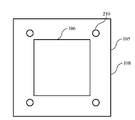
[0012] 도 2는 본 기술의 일부 실시예들에 따른 예시적인 포토마스크의 개략적인 평면도를 도시한다.
[0013] 도 3은 본 기술의 일부 실시예들에 따른, 포토마스크를 세정하는 방법의 예시적인 동작들을 도시한다.
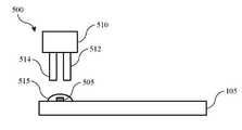
[0014] 도 4는 본 기술의 일부 실시예들에 따른 가열 동작의 개략적인 입면도를 도시한다.
[0015] 도 5는 본 기술의 일부 실시예들에 따른 에칭 동작의 개략적인 입면도를 도시한다.
[0016] 도 6은 본 기술의 일부 실시예들에 따른 린싱 동작의 개략적인 입면도를 도시한다.
[0017] 도면들 중 몇몇 도면들은 개략도들로서 포함된다. 도면들은 예시적인 목적들을 위한 것이며, 스케일링된 것으로 구체적으로 명시되지 않는 한, 스케일링된 것으로 간주되지 않아야 한다는 것이 이해되어야 한다. 부가적으로, 개략도들로서, 도면들은 이해를 돕기 위해 제공되며, 현실적인 표현들과 비교하여 모든 양상들 또는 정보를 포함하지 않을 수 있고, 예시적인 목적들을 위해 과장된 자료를 포함할 수 있다.
[0018] 도면들에서, 유사한 컴포넌트들 및/또는 피처들은 동일한 수치 참조 라벨을 가질 수 있다. 추가로, 동일한 타입의 다양한 컴포넌트들은, 유사한 컴포넌트들 및/또는 피처들을 구별하는 문자를 참조 라벨에 뒤따르게 함으로써 구별될 수 있다. 본 명세서에서 제1 수치 참조 라벨만이 사용되는 경우, 설명은 문자 접미사와 무관하게, 동일한 제1 수치 참조 라벨을 갖는 유사한 컴포넌트들 및/또는 피처들 중 어떠한 컴포넌트에도 적용가능하다.
Claims (15)
- 포토마스크를 세정하는 방법으로서,
상기 포토마스크의 표면 상의 잔류 커플링 재료(residual coupling material)를 가열하는 단계 ― 상기 포토마스크는 활성 구역들 및 에지 구역들을 특징으로 하고, 상기 잔류 커플링 재료는 상기 에지 구역들 위에 놓인 상기 포토마스크의 부분들 상에 위치됨 ―;
상기 잔류 커플링 재료에 에천트를 적용(apply)하는 단계; 및
상기 포토마스크로부터 상기 에천트를 린싱(rinse)하는 단계
를 포함하며,
상기 포토마스크의 활성 구역들의 일부는 상기 방법 동안 상기 에천트가 실질적으로 없는 상태로 유지되는,
포토마스크를 세정하는 방법. - 제1 항에 있어서,
상기 가열은, 상기 포토마스크를 약 150 ℃ 미만의 온도로 유지하면서, 상기 잔류 커플링 재료의 온도를 약 200 ℃ 초과로 상승시키는,
포토마스크를 세정하는 방법. - 제1 항에 있어서,
상기 가열은 상기 잔류 커플링 재료 근처에 적용되는 국부화된 가열을 포함하며,
상기 가열은, 상기 잔류 커플링 재료의 직경보다 500% 미만만큼 더 큰 직경을 특징으로 하는, 상기 포토마스크의 구역 내에 억제(contain)되는,
포토마스크를 세정하는 방법. - 제1 항에 있어서,
상기 에천트는 황산 및 과산화 수소를 포함하는,
포토마스크를 세정하는 방법. - 제4 항에 있어서,
상기 에천트를 적용하는 단계는, 상기 황산 및 상기 과산화 수소를 순차적으로 적용하는 단계를 포함하는,
포토마스크를 세정하는 방법. - 제5 항에 있어서,
상기 황산은 상기 과산화 수소 전에 적용되며,
상기 과산화 수소는 적어도 약 2초의 지연 후에 상기 황산에 적용되는,
포토마스크를 세정하는 방법. - 제4 항에 있어서,
상기 에천트는 각각 약 5 mL 미만의 상기 황산 및 상기 과산화 수소를 포함하는,
포토마스크를 세정하는 방법. - 제1 항에 있어서,
상기 린싱하는 단계는, 상기 에천트를 제거하기 위해 상기 포토마스크에 탈이온수를 전달하는 단계를 포함하는,
포토마스크를 세정하는 방법. - 제8 항에 있어서,
상기 탈이온수는, 상기 포토마스크의 활성 구역들에서 에천트 접촉을 제한하기 위해, 상기 포토마스크 상의 중앙 위치에 적용되고, 상기 에천트를 향해 측방향 외측으로 유동하게 되는,
포토마스크를 세정하는 방법. - 제9 항에 있어서,
상기 포토마스크는 상기 린싱 동안 회전되는,
포토마스크를 세정하는 방법. - 포토마스크를 세정하는 방법으로서,
상기 포토마스크의 표면 상의 잔류 커플링 재료를 가열하는 단계 ― 상기 포토마스크는 활성 구역들 및 에지 구역들을 특징으로 하고, 상기 잔류 커플링 재료는 상기 포토마스크의 에지 구역들 상에 위치됨 ―;
상기 잔류 커플링 재료에 액체 에천트를 전달하는 단계 ― 상기 전달은, 상기 가열된 잔류 커플링 재료가 내부에 있는, 약 10 cm2 미만의 상기 포토마스크의 표면 영역 내에 억제됨 ―;
상기 포토마스크로부터 상기 에천트를 린싱하는 단계 ― 상기 포토마스크의 활성 구역들의 일부는, 상기 액체 에천트의 전달 및 상기 린싱 동작들 동안, 상기 에천트가 실질적으로 없는 상태로 유지됨 ―; 및
상기 포토마스크를 건조시키는 단계
를 포함하는,
포토마스크를 세정하는 방법. - 제11 항에 있어서,
상기 방법은 약 20분 이하 내에 수행되며,
상기 린싱은 상기 액체 에천트를 전달하고 5분 미만 후에 수행되는,
포토마스크를 세정하는 방법. - 제11 항에 있어서,
상기 액체 에천트를 전달하는 단계는, 상기 가열된 커플링 재료에 황산 및 과산화 수소를 순차적으로 적용하는 단계를 포함하는,
포토마스크를 세정하는 방법. - 제11 항에 있어서,
상기 가열은, 열 램프에 의해, 약 2분 이하의 시간 기간 동안 그리고 약 200 ℃ 이상의 온도까지 수행되는,
포토마스크를 세정하는 방법. - 제11 항에 있어서,
상기 린싱하는 단계는, 상기 에천트가 상부에 위치된, 상기 포토마스크 상의 위치의 반경방향 내측에서 상기 포토마스크에 린스제를 전달하는 단계를 포함하는,
포토마스크를 세정하는 방법.
Applications Claiming Priority (3)
| Application Number | Priority Date | Filing Date | Title |
|---|---|---|---|
| US201762556736P | 2017-09-11 | 2017-09-11 | |
| US62/556,736 | 2017-09-11 | ||
| PCT/US2018/050152 WO2019051348A1 (en) | 2017-09-11 | 2018-09-10 | METHODS OF CLEANING PHOTOGRAPHIC MASK |
Publications (2)
| Publication Number | Publication Date |
|---|---|
| KR20200039849A true KR20200039849A (ko) | 2020-04-16 |
| KR102418491B1 KR102418491B1 (ko) | 2022-07-06 |
Family
ID=65631029
Family Applications (1)
| Application Number | Title | Priority Date | Filing Date |
|---|---|---|---|
| KR1020207010352A Active KR102418491B1 (ko) | 2017-09-11 | 2018-09-10 | 포토마스크 세정 프로세스들 |
Country Status (5)
| Country | Link |
|---|---|
| US (1) | US10816895B2 (ko) |
| KR (1) | KR102418491B1 (ko) |
| CN (1) | CN111051989B (ko) |
| TW (1) | TWI782077B (ko) |
| WO (1) | WO2019051348A1 (ko) |
Cited By (1)
| Publication number | Priority date | Publication date | Assignee | Title |
|---|---|---|---|---|
| KR20240008072A (ko) * | 2022-07-11 | 2024-01-18 | 주식회사 에프에스티 | 펠리클 프레임의 제조방법 |
Families Citing this family (14)
| Publication number | Priority date | Publication date | Assignee | Title |
|---|---|---|---|---|
| US10276411B2 (en) | 2017-08-18 | 2019-04-30 | Applied Materials, Inc. | High pressure and high temperature anneal chamber |
| US11028480B2 (en) | 2018-03-19 | 2021-06-08 | Applied Materials, Inc. | Methods of protecting metallic components against corrosion using chromium-containing thin films |
| US11015252B2 (en) | 2018-04-27 | 2021-05-25 | Applied Materials, Inc. | Protection of components from corrosion |
| US11009339B2 (en) | 2018-08-23 | 2021-05-18 | Applied Materials, Inc. | Measurement of thickness of thermal barrier coatings using 3D imaging and surface subtraction methods for objects with complex geometries |
| CN113795908B (zh) | 2019-04-08 | 2025-06-20 | 应用材料公司 | 用于修改光刻胶轮廓和调整临界尺寸的方法 |
| US11629402B2 (en) | 2019-04-16 | 2023-04-18 | Applied Materials, Inc. | Atomic layer deposition on optical structures |
| US11572619B2 (en) | 2019-04-16 | 2023-02-07 | Applied Materials, Inc. | Method of thin film deposition in trenches |
| WO2020219332A1 (en) | 2019-04-26 | 2020-10-29 | Applied Materials, Inc. | Methods of protecting aerospace components against corrosion and oxidation |
| US11794382B2 (en) | 2019-05-16 | 2023-10-24 | Applied Materials, Inc. | Methods for depositing anti-coking protective coatings on aerospace components |
| US11697879B2 (en) | 2019-06-14 | 2023-07-11 | Applied Materials, Inc. | Methods for depositing sacrificial coatings on aerospace components |
| US11466364B2 (en) | 2019-09-06 | 2022-10-11 | Applied Materials, Inc. | Methods for forming protective coatings containing crystallized aluminum oxide |
| US11519066B2 (en) | 2020-05-21 | 2022-12-06 | Applied Materials, Inc. | Nitride protective coatings on aerospace components and methods for making the same |
| US11739429B2 (en) | 2020-07-03 | 2023-08-29 | Applied Materials, Inc. | Methods for refurbishing aerospace components |
| US12461440B2 (en) * | 2022-06-30 | 2025-11-04 | Taiwan Semiconductor Manufacturing Company, Ltd. | Pellicle membrane with improved properties |
Citations (4)
| Publication number | Priority date | Publication date | Assignee | Title |
|---|---|---|---|---|
| JP2004349669A (ja) * | 2003-03-26 | 2004-12-09 | Dainippon Screen Mfg Co Ltd | 基板処理装置および基板処理方法 |
| KR20110013705A (ko) * | 2009-08-03 | 2011-02-10 | 삼성전자주식회사 | 블로잉을 이용한 포토 마스크의 세정 방법 및 장치 |
| US20110146727A1 (en) * | 2008-08-13 | 2011-06-23 | Kalyankar Nikhil D | Combinatorial approach to the development of cleaning formulations for glue removal in semiconductor applications |
| KR20120097104A (ko) * | 2011-02-24 | 2012-09-03 | 삼성전자주식회사 | 자외선 세정 장치 및 이를 이용한 세정 방법 |
Family Cites Families (12)
| Publication number | Priority date | Publication date | Assignee | Title |
|---|---|---|---|---|
| JP3920429B2 (ja) * | 1997-12-02 | 2007-05-30 | 株式会社ルネサステクノロジ | 位相シフトフォトマスクの洗浄方法および洗浄装置 |
| US7780867B1 (en) * | 1999-10-01 | 2010-08-24 | Novellus Systems, Inc. | Edge bevel removal of copper from silicon wafers |
| TWI377453B (en) * | 2003-07-31 | 2012-11-21 | Akrion Technologies Inc | Process sequence for photoresist stripping and/or cleaning of photomasks for integrated circuit manufacturing |
| US20070068558A1 (en) * | 2005-09-06 | 2007-03-29 | Applied Materials, Inc. | Apparatus and methods for mask cleaning |
| DE602005012111D1 (de) * | 2005-10-21 | 2009-02-12 | Advanced Mask Technology Ct Gmbh | Verfahren zur Reinigung der Oberfläche einer Photomaske |
| EP1832353A3 (fr) * | 2006-03-08 | 2009-05-06 | St Microelectronics S.A. | Nettoyage de masques de photolithographie |
| KR20080001469A (ko) * | 2006-06-29 | 2008-01-03 | 주식회사 하이닉스반도체 | 포토 마스크의 펠리클 재작업 방법 |
| JP2013068786A (ja) | 2011-09-22 | 2013-04-18 | Toppan Printing Co Ltd | フォトマスクの洗浄方法 |
| US8697573B2 (en) * | 2011-11-09 | 2014-04-15 | Intermolecular, Inc. | Process to remove Ni and Pt residues for NiPtSi applications using aqua regia with microwave assisted heating |
| US9627234B2 (en) | 2013-03-14 | 2017-04-18 | Taiwan Semiconductor Manufacturing Company, Ltd. | Method and apparatus for localized and controlled removal of material from a substrate |
| KR20150044765A (ko) * | 2013-10-17 | 2015-04-27 | 삼성전자주식회사 | 포토마스크 세정 방법 |
| JP2017077528A (ja) | 2015-10-20 | 2017-04-27 | 信越化学工業株式会社 | フォトマスク関連基板に用いる基板洗浄装置及び基板洗浄方法 |
-
2018
- 2018-08-22 TW TW107129202A patent/TWI782077B/zh active
- 2018-09-10 CN CN201880057184.1A patent/CN111051989B/zh active Active
- 2018-09-10 WO PCT/US2018/050152 patent/WO2019051348A1/en not_active Ceased
- 2018-09-10 US US16/126,046 patent/US10816895B2/en active Active
- 2018-09-10 KR KR1020207010352A patent/KR102418491B1/ko active Active
Patent Citations (4)
| Publication number | Priority date | Publication date | Assignee | Title |
|---|---|---|---|---|
| JP2004349669A (ja) * | 2003-03-26 | 2004-12-09 | Dainippon Screen Mfg Co Ltd | 基板処理装置および基板処理方法 |
| US20110146727A1 (en) * | 2008-08-13 | 2011-06-23 | Kalyankar Nikhil D | Combinatorial approach to the development of cleaning formulations for glue removal in semiconductor applications |
| KR20110013705A (ko) * | 2009-08-03 | 2011-02-10 | 삼성전자주식회사 | 블로잉을 이용한 포토 마스크의 세정 방법 및 장치 |
| KR20120097104A (ko) * | 2011-02-24 | 2012-09-03 | 삼성전자주식회사 | 자외선 세정 장치 및 이를 이용한 세정 방법 |
Cited By (1)
| Publication number | Priority date | Publication date | Assignee | Title |
|---|---|---|---|---|
| KR20240008072A (ko) * | 2022-07-11 | 2024-01-18 | 주식회사 에프에스티 | 펠리클 프레임의 제조방법 |
Also Published As
| Publication number | Publication date |
|---|---|
| WO2019051348A1 (en) | 2019-03-14 |
| US10816895B2 (en) | 2020-10-27 |
| CN111051989B (zh) | 2022-09-27 |
| CN111051989A (zh) | 2020-04-21 |
| TW201921434A (zh) | 2019-06-01 |
| TWI782077B (zh) | 2022-11-01 |
| US20190079388A1 (en) | 2019-03-14 |
| KR102418491B1 (ko) | 2022-07-06 |
Similar Documents
| Publication | Publication Date | Title |
|---|---|---|
| KR102418491B1 (ko) | 포토마스크 세정 프로세스들 | |
| JP6000822B2 (ja) | 基板洗浄方法および基板洗浄システム | |
| TWI600056B (zh) | Substrate cleaning device and substrate cleaning method | |
| JP5543633B2 (ja) | 基板洗浄システム、基板洗浄方法および記憶媒体 | |
| JP5977727B2 (ja) | 基板洗浄方法、基板洗浄システムおよび記憶媒体 | |
| JP6356295B2 (ja) | 基板洗浄装置、基板洗浄方法および記憶媒体 | |
| US20110132394A1 (en) | Method and Apparatus for an In-Situ Ultraviolet Cleaning Tool | |
| JP4583515B2 (ja) | チャック洗浄を用いて基板上の粒子を減少させる方法 | |
| KR101461437B1 (ko) | 포토마스크 세정 장치 및 이를 이용한 포토마스크 세정 방법 | |
| JP6279037B2 (ja) | 基板洗浄方法および基板洗浄システム | |
| JP2011129583A (ja) | 半導体基板の表面処理装置及び方法 | |
| JP2014197717A (ja) | 基板洗浄装置、基板洗浄システム、基板洗浄方法および記憶媒体 | |
| JP5305300B2 (ja) | フォトマスクの製造方法、パターン転写方法、フォトマスク基板用処理装置、及び薄膜パターニング方法 | |
| JP2017147329A (ja) | 基板処理装置および基板処理方法 | |
| KR101216797B1 (ko) | 기판 처리 방법, euv 마스크의 제조 방법 및 euv 마스크 | |
| JP2009099856A (ja) | 基板処理方法及び基板処理装置 | |
| JP4519234B2 (ja) | 物品表面の清浄化方法およびそのための清浄化装置 | |
| JP2004071966A (ja) | レジスト剥離方法 | |
| JP2005266534A (ja) | マスク基板用レジスト除去装置 | |
| JP2008244323A (ja) | ステンシルマスク | |
| JP2011206720A (ja) | ドライ完結型有機el用マスククリーナ装置及びそのためのマスククリーニング方法 | |
| CN104238280A (zh) | 半导体装置的制造方法 |
Legal Events
| Date | Code | Title | Description |
|---|---|---|---|
| PA0105 | International application |
St.27 status event code: A-0-1-A10-A15-nap-PA0105 |
|
| PA0201 | Request for examination |
St.27 status event code: A-1-2-D10-D11-exm-PA0201 |
|
| PG1501 | Laying open of application |
St.27 status event code: A-1-1-Q10-Q12-nap-PG1501 |
|
| D13-X000 | Search requested |
St.27 status event code: A-1-2-D10-D13-srh-X000 |
|
| D14-X000 | Search report completed |
St.27 status event code: A-1-2-D10-D14-srh-X000 |
|
| E902 | Notification of reason for refusal | ||
| PE0902 | Notice of grounds for rejection |
St.27 status event code: A-1-2-D10-D21-exm-PE0902 |
|
| E13-X000 | Pre-grant limitation requested |
St.27 status event code: A-2-3-E10-E13-lim-X000 |
|
| P11-X000 | Amendment of application requested |
St.27 status event code: A-2-2-P10-P11-nap-X000 |
|
| P13-X000 | Application amended |
St.27 status event code: A-2-2-P10-P13-nap-X000 |
|
| E701 | Decision to grant or registration of patent right | ||
| PE0701 | Decision of registration |
St.27 status event code: A-1-2-D10-D22-exm-PE0701 |
|
| GRNT | Written decision to grant | ||
| PR0701 | Registration of establishment |
St.27 status event code: A-2-4-F10-F11-exm-PR0701 |
|
| PR1002 | Payment of registration fee |
St.27 status event code: A-2-2-U10-U12-oth-PR1002 Fee payment year number: 1 |
|
| PG1601 | Publication of registration |
St.27 status event code: A-4-4-Q10-Q13-nap-PG1601 |
|
| R17 | Change to representative recorded |
Free format text: ST27 STATUS EVENT CODE: A-5-5-R10-R17-OTH-X000 (AS PROVIDED BY THE NATIONAL OFFICE) |
|
| R17-X000 | Change to representative recorded |
St.27 status event code: A-5-5-R10-R17-oth-X000 |
|
| P22-X000 | Classification modified |
St.27 status event code: A-4-4-P10-P22-nap-X000 |