KR20200039900A - 화소 및 표시 장치 - Google Patents
화소 및 표시 장치 Download PDFInfo
- Publication number
- KR20200039900A KR20200039900A KR1020180119300A KR20180119300A KR20200039900A KR 20200039900 A KR20200039900 A KR 20200039900A KR 1020180119300 A KR1020180119300 A KR 1020180119300A KR 20180119300 A KR20180119300 A KR 20180119300A KR 20200039900 A KR20200039900 A KR 20200039900A
- Authority
- KR
- South Korea
- Prior art keywords
- light emitting
- electrode
- control signal
- transistors
- emitting elements
- Prior art date
- Legal status (The legal status is an assumption and is not a legal conclusion. Google has not performed a legal analysis and makes no representation as to the accuracy of the status listed.)
- Granted
Links
Images





Classifications
-
- G—PHYSICS
- G09—EDUCATION; CRYPTOGRAPHY; DISPLAY; ADVERTISING; SEALS
- G09G—ARRANGEMENTS OR CIRCUITS FOR CONTROL OF INDICATING DEVICES USING STATIC MEANS TO PRESENT VARIABLE INFORMATION
- G09G3/00—Control arrangements or circuits, of interest only in connection with visual indicators other than cathode-ray tubes
- G09G3/20—Control arrangements or circuits, of interest only in connection with visual indicators other than cathode-ray tubes for presentation of an assembly of a number of characters, e.g. a page, by composing the assembly by combination of individual elements arranged in a matrix no fixed position being assigned to or needed to be assigned to the individual characters or partial characters
- G09G3/22—Control arrangements or circuits, of interest only in connection with visual indicators other than cathode-ray tubes for presentation of an assembly of a number of characters, e.g. a page, by composing the assembly by combination of individual elements arranged in a matrix no fixed position being assigned to or needed to be assigned to the individual characters or partial characters using controlled light sources
- G09G3/30—Control arrangements or circuits, of interest only in connection with visual indicators other than cathode-ray tubes for presentation of an assembly of a number of characters, e.g. a page, by composing the assembly by combination of individual elements arranged in a matrix no fixed position being assigned to or needed to be assigned to the individual characters or partial characters using controlled light sources using electroluminescent panels
- G09G3/32—Control arrangements or circuits, of interest only in connection with visual indicators other than cathode-ray tubes for presentation of an assembly of a number of characters, e.g. a page, by composing the assembly by combination of individual elements arranged in a matrix no fixed position being assigned to or needed to be assigned to the individual characters or partial characters using controlled light sources using electroluminescent panels semiconductive, e.g. using light-emitting diodes [LED]
- G09G3/3208—Control arrangements or circuits, of interest only in connection with visual indicators other than cathode-ray tubes for presentation of an assembly of a number of characters, e.g. a page, by composing the assembly by combination of individual elements arranged in a matrix no fixed position being assigned to or needed to be assigned to the individual characters or partial characters using controlled light sources using electroluminescent panels semiconductive, e.g. using light-emitting diodes [LED] organic, e.g. using organic light-emitting diodes [OLED]
- G09G3/3225—Control arrangements or circuits, of interest only in connection with visual indicators other than cathode-ray tubes for presentation of an assembly of a number of characters, e.g. a page, by composing the assembly by combination of individual elements arranged in a matrix no fixed position being assigned to or needed to be assigned to the individual characters or partial characters using controlled light sources using electroluminescent panels semiconductive, e.g. using light-emitting diodes [LED] organic, e.g. using organic light-emitting diodes [OLED] using an active matrix
- G09G3/3233—Control arrangements or circuits, of interest only in connection with visual indicators other than cathode-ray tubes for presentation of an assembly of a number of characters, e.g. a page, by composing the assembly by combination of individual elements arranged in a matrix no fixed position being assigned to or needed to be assigned to the individual characters or partial characters using controlled light sources using electroluminescent panels semiconductive, e.g. using light-emitting diodes [LED] organic, e.g. using organic light-emitting diodes [OLED] using an active matrix with pixel circuitry controlling the current through the light-emitting element
-
- G—PHYSICS
- G09—EDUCATION; CRYPTOGRAPHY; DISPLAY; ADVERTISING; SEALS
- G09G—ARRANGEMENTS OR CIRCUITS FOR CONTROL OF INDICATING DEVICES USING STATIC MEANS TO PRESENT VARIABLE INFORMATION
- G09G3/00—Control arrangements or circuits, of interest only in connection with visual indicators other than cathode-ray tubes
- G09G3/20—Control arrangements or circuits, of interest only in connection with visual indicators other than cathode-ray tubes for presentation of an assembly of a number of characters, e.g. a page, by composing the assembly by combination of individual elements arranged in a matrix no fixed position being assigned to or needed to be assigned to the individual characters or partial characters
- G09G3/22—Control arrangements or circuits, of interest only in connection with visual indicators other than cathode-ray tubes for presentation of an assembly of a number of characters, e.g. a page, by composing the assembly by combination of individual elements arranged in a matrix no fixed position being assigned to or needed to be assigned to the individual characters or partial characters using controlled light sources
- G09G3/30—Control arrangements or circuits, of interest only in connection with visual indicators other than cathode-ray tubes for presentation of an assembly of a number of characters, e.g. a page, by composing the assembly by combination of individual elements arranged in a matrix no fixed position being assigned to or needed to be assigned to the individual characters or partial characters using controlled light sources using electroluminescent panels
- G09G3/32—Control arrangements or circuits, of interest only in connection with visual indicators other than cathode-ray tubes for presentation of an assembly of a number of characters, e.g. a page, by composing the assembly by combination of individual elements arranged in a matrix no fixed position being assigned to or needed to be assigned to the individual characters or partial characters using controlled light sources using electroluminescent panels semiconductive, e.g. using light-emitting diodes [LED]
-
- G—PHYSICS
- G09—EDUCATION; CRYPTOGRAPHY; DISPLAY; ADVERTISING; SEALS
- G09G—ARRANGEMENTS OR CIRCUITS FOR CONTROL OF INDICATING DEVICES USING STATIC MEANS TO PRESENT VARIABLE INFORMATION
- G09G2300/00—Aspects of the constitution of display devices
- G09G2300/08—Active matrix structure, i.e. with use of active elements, inclusive of non-linear two terminal elements, in the pixels together with light emitting or modulating elements
- G09G2300/0804—Sub-multiplexed active matrix panel, i.e. wherein one active driving circuit is used at pixel level for multiple image producing elements
-
- G—PHYSICS
- G09—EDUCATION; CRYPTOGRAPHY; DISPLAY; ADVERTISING; SEALS
- G09G—ARRANGEMENTS OR CIRCUITS FOR CONTROL OF INDICATING DEVICES USING STATIC MEANS TO PRESENT VARIABLE INFORMATION
- G09G2300/00—Aspects of the constitution of display devices
- G09G2300/08—Active matrix structure, i.e. with use of active elements, inclusive of non-linear two terminal elements, in the pixels together with light emitting or modulating elements
- G09G2300/0809—Several active elements per pixel in active matrix panels
-
- G—PHYSICS
- G09—EDUCATION; CRYPTOGRAPHY; DISPLAY; ADVERTISING; SEALS
- G09G—ARRANGEMENTS OR CIRCUITS FOR CONTROL OF INDICATING DEVICES USING STATIC MEANS TO PRESENT VARIABLE INFORMATION
- G09G2300/00—Aspects of the constitution of display devices
- G09G2300/08—Active matrix structure, i.e. with use of active elements, inclusive of non-linear two terminal elements, in the pixels together with light emitting or modulating elements
- G09G2300/0809—Several active elements per pixel in active matrix panels
- G09G2300/0819—Several active elements per pixel in active matrix panels used for counteracting undesired variations, e.g. feedback or autozeroing
-
- G—PHYSICS
- G09—EDUCATION; CRYPTOGRAPHY; DISPLAY; ADVERTISING; SEALS
- G09G—ARRANGEMENTS OR CIRCUITS FOR CONTROL OF INDICATING DEVICES USING STATIC MEANS TO PRESENT VARIABLE INFORMATION
- G09G2300/00—Aspects of the constitution of display devices
- G09G2300/08—Active matrix structure, i.e. with use of active elements, inclusive of non-linear two terminal elements, in the pixels together with light emitting or modulating elements
- G09G2300/0809—Several active elements per pixel in active matrix panels
- G09G2300/0823—Several active elements per pixel in active matrix panels used to establish symmetry in driving, e.g. with polarity inversion
-
- G—PHYSICS
- G09—EDUCATION; CRYPTOGRAPHY; DISPLAY; ADVERTISING; SEALS
- G09G—ARRANGEMENTS OR CIRCUITS FOR CONTROL OF INDICATING DEVICES USING STATIC MEANS TO PRESENT VARIABLE INFORMATION
- G09G2300/00—Aspects of the constitution of display devices
- G09G2300/08—Active matrix structure, i.e. with use of active elements, inclusive of non-linear two terminal elements, in the pixels together with light emitting or modulating elements
- G09G2300/0809—Several active elements per pixel in active matrix panels
- G09G2300/0842—Several active elements per pixel in active matrix panels forming a memory circuit, e.g. a dynamic memory with one capacitor
-
- G—PHYSICS
- G09—EDUCATION; CRYPTOGRAPHY; DISPLAY; ADVERTISING; SEALS
- G09G—ARRANGEMENTS OR CIRCUITS FOR CONTROL OF INDICATING DEVICES USING STATIC MEANS TO PRESENT VARIABLE INFORMATION
- G09G2310/00—Command of the display device
- G09G2310/02—Addressing, scanning or driving the display screen or processing steps related thereto
- G09G2310/0264—Details of driving circuits
-
- G—PHYSICS
- G09—EDUCATION; CRYPTOGRAPHY; DISPLAY; ADVERTISING; SEALS
- G09G—ARRANGEMENTS OR CIRCUITS FOR CONTROL OF INDICATING DEVICES USING STATIC MEANS TO PRESENT VARIABLE INFORMATION
- G09G2320/00—Control of display operating conditions
- G09G2320/02—Improving the quality of display appearance
- G09G2320/0233—Improving the luminance or brightness uniformity across the screen
-
- G—PHYSICS
- G09—EDUCATION; CRYPTOGRAPHY; DISPLAY; ADVERTISING; SEALS
- G09G—ARRANGEMENTS OR CIRCUITS FOR CONTROL OF INDICATING DEVICES USING STATIC MEANS TO PRESENT VARIABLE INFORMATION
- G09G2320/00—Control of display operating conditions
- G09G2320/06—Adjustment of display parameters
- G09G2320/0626—Adjustment of display parameters for control of overall brightness
Landscapes
- Engineering & Computer Science (AREA)
- Physics & Mathematics (AREA)
- Computer Hardware Design (AREA)
- General Physics & Mathematics (AREA)
- Theoretical Computer Science (AREA)
- Control Of Indicators Other Than Cathode Ray Tubes (AREA)
- Control Of El Displays (AREA)
- Electroluminescent Light Sources (AREA)
Abstract
Description
도 2는 일 실시예에 따른 화소의 개략적인 블록도이다.
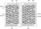
도 3은 일 실시예에 따른 발광부의 개략적인 평면도를 도시한다.
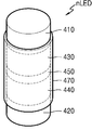
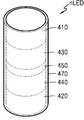
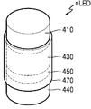
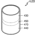
도 4a 내지 도 4d는 다양한 실시예들에 따른 발광 소자들을 도시한다.
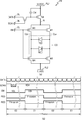
도 5는 일 실시예에 따른 발광 회로들의 회로도 및 타이밍도를 도시한다.
도 6은 다른 실시예에 따른 발광 회로들의 회로도 및 타이밍도를 도시한다.
도 7a 내지 도 7c는 다양한 실시예들에 따른 화소 회로들의 회로도를 도시한다.
도 8은 일 실시예에 따라서 예시적인 화소의 회로도 및 타이밍도를 도시한다.
도 9는 다양한 실시예들에 따라서 정렬도가 다른 화소들의 인지 휘도를 나타내는 그래프들이다.
Claims (20)
- 제1 방향과 제2 방향으로 배열되는 복수의 화소들을 포함하는 표시부;
복수의 주사선들을 통해 상기 복수의 화소들에 주사 신호들을 전달하는 주사 구동부;
복수의 데이터선들을 통해 상기 복수의 화소들에 데이터 전압들을 전달하는 데이터 구동부;
제어선을 통해 상기 복수의 화소들에 제어 신호를 전달하는 제어 구동부; 및
제1 및 제2 전원선들을 통해 상기 복수의 화소들에 제1 및 제2 구동 전압들을 각각 공급하는 전압 생성부를 포함하고,
상기 화소들 각각은,
제1 전극과 제2 전극 사이에 정방향으로 연결되는 제1 발광 소자들과 역방향으로 연결되는 제2 발광 소자들을 포함하는 발광부;
상기 주사 신호들 중에서 대응하는 주사 신호에 동기화하여 상기 데이터 전압들 중에서 대응하는 데이터 전압을 수신하고, 상기 데이터 전압에 기초하여 구동 전류를 생성하여 제1 노드에 출력하는 화소 회로; 및
상기 제어 신호에 의해 제어되며, 제1 발광 구간 동안 상기 구동 전류를 상기 제1 발광 소자들에게 제공하고, 제2 발광 구간 동안 상기 구동 전류를 상기 제2 발광 소자들에게 제공하는 발광 회로를 포함하는 표시 장치. - 제1 항에 있어서,
상기 제1 및 제2 발광 소자들은 초소형 발광 다이오드(micro LED)이고,
상기 제1 발광 소자들 각각은 상기 제1 전극에 접속하는 애노드 및 상기 제2 전극에 접속하는 캐소드를 갖고,
상기 제2 발광 소자들 각각은 상기 제2 전극에 접속하는 애노드 및 상기 제1 전극에 접속하는 캐소드를 갖는 것을 특징으로 하는 표시 장치. - 제1 항에 있어서,
상기 화소들 각각에서 상기 제1 발광 소자들의 개수에 대한 상기 제2 발광 소자들의 개수의 비율은 일정하지 않은 것을 특징으로 하는 표시 장치. - 제1 항에 있어서,
상기 화소들 각각은 한 프레임 기간 동안 복수의 상기 제1 발광 구간과 복수의 상기 제2 발광 구간을 교대로 갖는 것을 특징으로 하는 표시 장치. - 제1 항에 있어서,
상기 발광 회로는,
상기 제1 노드와 상기 제1 전극 사이에 연결되는 제1 트랜지스터;
상기 제1 노드와 상기 제2 전극 사이에 연결되는 제2 트랜지스터;
상기 제1 전극과 상기 제2 전원선 사이에 연결되는 제3 트랜지스터; 및
상기 제2 전극과 상기 제2 전원선 사이에 연결되는 제4 트랜지스터를 포함하는 것을 특징으로 하는 표시 장치. - 제5 항에 있어서,
상기 제1 및 제4 트랜지스터들의 도전형은 상기 제2 및 제3 트랜지스터들의 도전형과 반대이고,
상기 제1 내지 제4 트랜지스터들 각각의 게이트 전극은 상기 제어선에 공통적으로 연결되는 것을 특징으로 하는 표시 장치. - 제6 항에 있어서,
상기 제어 구동부는,
상기 제1 발광 구간 동안, 상기 제1 및 제4 트랜지스터들이 턴 온되고 상기 제2 및 제3 트랜지스터들이 턴 오프되어 상기 구동 전류가 상기 제1 발광 소자들을 통해 흐르도록, 제1 논리 레벨을 갖는 상기 제어 신호를 상기 제어선에 출력하고,
상기 제2 발광 구간 동안, 상기 제2 및 제3 트랜지스터들이 턴 온되고 상기 제1 및 제4 트랜지스터들이 턴 오프되어 상기 구동 전류가 상기 제2 발광 소자들을 통해 흐르도록, 제2 논리 레벨을 갖는 상기 제어 신호를 상기 제어선에 출력하는 것을 특징으로 하는 표시 장치. - 제7 항에 있어서,
상기 제어 구동부는 한 프레임 기간 동안 상기 제1 논리 레벨을 갖는 상기 제어 신호와 상기 제2 논리 레벨을 갖는 상기 제어 신호를 교대로 복수 회 출력하는 것을 특징으로 하는 표시 장치. - 제5 항에 있어서,
상기 제어선은 상기 복수의 화소들에 제1 제어 신호를 전달하는 제1 제어선, 및 상기 복수의 화소들에 제2 제어 신호를 전달하는 제2 제어선을 포함하고,
상기 제1 및 제4 트랜지스터들 각각의 게이트 전극은 상기 제1 제어선에 공통적으로 연결되고,
상기 제2 및 제3 트랜지스터들 각각의 게이트 전극은 상기 제2 제어선에 공통적으로 연결되는 것을 특징으로 하는 표시 장치. - 제9 항에 있어서,
상기 제어 구동부는,
상기 제1 발광 구간 동안, 턴 온 레벨을 갖는 상기 제1 제어 신호를 상기 제1 제어선에 출력하고 턴 오프 레벨을 갖는 상기 제2 제어 신호를 상기 제2 제어선에 출력하며,
상기 제2 발광 구간 동안, 턴 온 레벨을 갖는 상기 제2 제어 신호를 상기 제2 제어선에 출력하고 턴 오프 레벨을 갖는 상기 제1 제어 신호를 상기 제1 제어선에 출력하는 것을 특징으로 하는 표시 장치. - 제10 항에 있어서,
상기 제어 구동부는 제1 듀티비로 상기 턴 온 레벨을 갖는 상기 제1 제어 신호 및 제2 듀티비로 상기 턴 온 레벨을 갖는 상기 제2 제어 신호를 상기 화소들 각각의 상기 발광 회로에 공통으로 출력하는 것을 특징으로 하는 표시 장치. - 제11 항에 있어서,
상기 제어 구동부를 통해 상기 제1 제어 신호의 상기 제1 듀티비와 상기 제2 제어 신호의 상기 제2 듀티비가 조절됨으로써, 상기 표시부의 전체 밝기가 조절되는 것을 특징으로 하는 표시 장치. - 주사 신호를 전달하는 주사선, 데이터 전압을 전달하는 데이터선, 제어 신호를 전달하는 제어선, 및 제1 및 제2 전원선들에 접속되는 화소에 있어서,
제1 전극과 제2 전극 사이에 정방향으로 연결되는 제1 발광 소자들과 역방향으로 연결되는 제2 발광 소자들을 포함하는 발광부;
상기 주사 신호에 동기화하여 상기 데이터 전압을 수신하고, 상기 데이터 전압에 기초하여 상기 제1 전원선으로부터 공급되는 제1 구동 전원으로부터 구동 전류를 생성하여 제1 노드에 출력하는 화소 회로; 및
상기 제1 및 제2 전극들, 상기 제1 노드, 상기 제2 전원선 및 상기 제어선에 연결되어 상기 제어 신호에 의해 제어되며, 제1 발광 구간 동안 상기 구동 전류를 상기 제1 발광 소자들에게 제공하고, 제2 발광 구간 동안 상기 구동 전류를 상기 제2 발광 소자들에게 제공하는 발광 회로를 포함하는 화소. - 제13 항에 있어서,
상기 발광 회로는,
상기 제1 노드와 상기 제1 전극 사이에 연결되는 제1 트랜지스터;
상기 제1 노드와 상기 제2 전극 사이에 연결되는 제2 트랜지스터;
상기 제1 전극과 상기 제2 전원선 사이에 연결되는 제3 트랜지스터; 및
상기 제2 전극과 상기 제2 전원선 사이에 연결되는 제4 트랜지스터를 포함하는 것을 특징으로 하는 화소. - 제14 항에 있어서,
상기 제1 내지 제4 트랜지스터들 각각의 게이트 전극은 상기 제어선에 공통적으로 연결되고,
상기 제1 및 제4 트랜지스터들은 제1 도전형의 트랜지스터이고, 상기 제2 및 제3 트랜지스터들은 상기 제1 도전형과 다른 제2 도전형의 트랜지스터인 것을 특징으로 하는 화소. - 제14 항에 있어서,
상기 제1 발광 구간 동안, 제1 논리 레벨을 갖는 상기 제어 신호에 의하여 상기 제1 및 제4 트랜지스터들은 턴 온되고 상기 제2 및 제3 트랜지스터들은 턴 오프됨으로써, 상기 구동 전류가 상기 제1 발광 소자들을 통해 흐르고,
상기 제2 발광 구간 동안, 제2 논리 레벨을 갖는 상기 제어 신호에 의하여 상기 제2 및 제3 트랜지스터들은 턴 온되고 상기 제1 및 제4 트랜지스터들은 턴 오프됨으로써, 상기 구동 전류가 상기 제2 발광 소자들을 통해 흐르는 것을 특징으로 하는 화소. - 제14 항에 있어서,
상기 제어선은 제1 제어 신호를 전달하는 제1 제어선, 및 제2 제어 신호를 전달하는 제2 제어선을 포함하고,
상기 제1 및 제4 트랜지스터들 각각의 게이트 전극은 상기 제1 제어선에 공통적으로 연결되고,
상기 제2 및 제3 트랜지스터들 각각의 게이트 전극은 상기 제2 제어선에 공통적으로 연결되는 것을 특징으로 하는 화소. - 제17 항에 있어서,
상기 제1 발광 구간 동안, 턴 온 레벨을 갖는 상기 제1 제어 신호에 의하여 상기 제1 및 제4 트랜지스터들이 턴 온되고 턴 오프 레벨을 갖는 상기 제2 제어 신호에 의해 상기 제2 및 제3 트랜지스터들이 턴 오프되어, 상기 구동 전류가 상기 제1 발광 소자들을 통해 흐르고,
상기 제2 발광 구간 동안, 턴 온 레벨을 갖는 상기 제2 제어 신호에 의하여 상기 제2 및 제3 트랜지스터들이 턴 온되고 턴 오프 레벨을 갖는 상기 제1 제어 신호에 의해 상기 제1 및 제4 트랜지스터들이 턴 오프되어, 상기 구동 전류가 상기 제2 발광 소자들을 통해 흐르는 것을 특징으로 하는 화소. - 제12 항에 있어서,
상기 화소 회로는,
상기 제1 전원선과 상기 제1 노드 사이에 연결되어 상기 데이터 전압에 따라 상기 구동 전류를 생성하는 구동 트랜지스터;
상기 데이터선과 상기 구동 트랜지스터의 게이트 전극 사이에 연결되고, 상기 주사 신호에 의해 제어되는 제1 스위칭 트랜지스터; 및
상기 구동 트랜지스터의 게이트 전극에 연결되어 상기 데이터 전압을 한 프레임 기간 동안 저장하는 저장 커패시터를 포함하는 것을 특징으로 하는 화소. - 제19 항에 있어서,
상기 화소 회로는 기준 전압을 전달하는 제3 전원선과 상기 제1 노드 사이에 연결되는 제2 스위칭 트랜지스터를 더 포함하고,
상기 저장 커패시터는 상기 구동 트랜지스터의 게이트 전극과 상기 제1 노드 사이에 연결되는 것을 특징으로 하는 화소.
Priority Applications (3)
| Application Number | Priority Date | Filing Date | Title |
|---|---|---|---|
| KR1020180119300A KR102584274B1 (ko) | 2018-10-05 | 2018-10-05 | 화소 및 표시 장치 |
| US16/546,205 US10964253B2 (en) | 2018-10-05 | 2019-08-20 | Pixel including light-emitting devices and display device including the pixel |
| CN201910795374.XA CN111028766B (zh) | 2018-10-05 | 2019-08-27 | 像素和显示装置 |
Applications Claiming Priority (1)
| Application Number | Priority Date | Filing Date | Title |
|---|---|---|---|
| KR1020180119300A KR102584274B1 (ko) | 2018-10-05 | 2018-10-05 | 화소 및 표시 장치 |
Publications (2)
| Publication Number | Publication Date |
|---|---|
| KR20200039900A true KR20200039900A (ko) | 2020-04-17 |
| KR102584274B1 KR102584274B1 (ko) | 2023-10-04 |
Family
ID=70052277
Family Applications (1)
| Application Number | Title | Priority Date | Filing Date |
|---|---|---|---|
| KR1020180119300A Active KR102584274B1 (ko) | 2018-10-05 | 2018-10-05 | 화소 및 표시 장치 |
Country Status (3)
| Country | Link |
|---|---|
| US (1) | US10964253B2 (ko) |
| KR (1) | KR102584274B1 (ko) |
| CN (1) | CN111028766B (ko) |
Cited By (3)
| Publication number | Priority date | Publication date | Assignee | Title |
|---|---|---|---|---|
| KR20210130311A (ko) * | 2020-04-21 | 2021-11-01 | 삼성디스플레이 주식회사 | 표시 장치 |
| WO2022010008A1 (ko) * | 2020-07-08 | 2022-01-13 | 엘지전자 주식회사 | 반도체 발광 소자를 이용한 디스플레이 장치 |
| WO2022085922A1 (ko) * | 2020-10-20 | 2022-04-28 | 삼성디스플레이 주식회사 | 화소 및 이를 구비한 표시 장치 |
Families Citing this family (3)
| Publication number | Priority date | Publication date | Assignee | Title |
|---|---|---|---|---|
| CN115482769A (zh) * | 2021-05-31 | 2022-12-16 | 京东方科技集团股份有限公司 | 像素驱动电路及其驱动方法、显示基板 |
| CN115331619B (zh) * | 2022-10-12 | 2023-01-31 | 惠科股份有限公司 | 像素驱动电路、显示面板及显示装置 |
| CN119339674A (zh) * | 2023-07-20 | 2025-01-21 | 京东方科技集团股份有限公司 | 像素电路及其控制方法、显示面板及显示装置 |
Citations (5)
| Publication number | Priority date | Publication date | Assignee | Title |
|---|---|---|---|---|
| KR20140111502A (ko) * | 2013-03-11 | 2014-09-19 | 삼성디스플레이 주식회사 | 표시장치 및 그 구동 방법 |
| KR101782889B1 (ko) * | 2016-07-21 | 2017-09-28 | 피에스아이 주식회사 | 휘도가 향상된 풀-컬러 led 디스플레이 및 그 제조방법 |
| KR20170132401A (ko) * | 2016-05-23 | 2017-12-04 | 삼성디스플레이 주식회사 | 표시 장치 및 이의 구동 방법 |
| KR101839953B1 (ko) * | 2011-01-21 | 2018-03-20 | 삼성디스플레이 주식회사 | 구동 장치 및 이를 이용한 표시 장치 |
| KR102448034B1 (ko) * | 2015-11-23 | 2022-09-28 | 삼성디스플레이 주식회사 | 화소 회로 및 이를 포함하는 유기 발광 표시 장치 |
Family Cites Families (21)
| Publication number | Priority date | Publication date | Assignee | Title |
|---|---|---|---|---|
| JP4914929B2 (ja) | 2009-10-15 | 2012-04-11 | シャープ株式会社 | 発光装置およびその製造方法 |
| KR20110041401A (ko) | 2009-10-15 | 2011-04-21 | 샤프 가부시키가이샤 | 발광 장치 및 그 제조 방법 |
| JP2012103538A (ja) * | 2010-11-11 | 2012-05-31 | Mitsumi Electric Co Ltd | バックライト装置、該装置を備えた画像表示システム、及び照明装置 |
| WO2013105003A1 (en) * | 2012-01-13 | 2013-07-18 | Koninklijke Philips N.V. | Led lighting unit with color and dimming control |
| CN103383834B (zh) * | 2013-07-02 | 2015-08-05 | 京东方科技集团股份有限公司 | 一种像素电路、显示面板及显示装置 |
| CN103383836B (zh) * | 2013-07-02 | 2015-05-27 | 京东方科技集团股份有限公司 | 一种像素电路及其驱动方法、显示面板及显示装置 |
| CN103413519B (zh) * | 2013-07-18 | 2016-05-11 | 京东方科技集团股份有限公司 | 一种像素电路及其驱动方法、阵列基板和显示装置 |
| CN203480806U (zh) * | 2013-07-18 | 2014-03-12 | 京东方科技集团股份有限公司 | 一种像素电路、阵列基板和显示装置 |
| CN103366682B (zh) | 2013-07-25 | 2015-06-17 | 京东方科技集团股份有限公司 | 一种交流驱动oled电路、驱动方法及显示装置 |
| CN103531149B (zh) | 2013-10-31 | 2015-07-15 | 京东方科技集团股份有限公司 | 一种交流驱动的像素电路、驱动方法及显示装置 |
| CN103531150B (zh) * | 2013-10-31 | 2015-06-10 | 京东方科技集团股份有限公司 | 一种交流驱动的像素电路、驱动方法及显示装置 |
| KR20150142943A (ko) * | 2014-06-12 | 2015-12-23 | 삼성디스플레이 주식회사 | 유기 발광 표시 장치 |
| KR102195993B1 (ko) * | 2014-10-31 | 2020-12-30 | 엘지디스플레이 주식회사 | 표시장치 및 이를 구비한 전자제품, 외부전원장치 |
| CN106782328A (zh) * | 2015-11-20 | 2017-05-31 | 上海和辉光电有限公司 | 一种像素电路 |
| CN205491361U (zh) * | 2015-12-29 | 2016-08-17 | 生迪智慧科技有限公司 | 可调节色温的led灯 |
| KR102592276B1 (ko) | 2016-07-15 | 2023-10-24 | 삼성디스플레이 주식회사 | 발광장치 및 그의 제조방법 |
| KR102701861B1 (ko) | 2016-11-15 | 2024-09-04 | 삼성디스플레이 주식회사 | 발광장치 및 그의 제조방법 |
| CN108449824B (zh) * | 2017-02-16 | 2020-06-23 | 朗德万斯公司 | Led模块和用于操作led模块的方法 |
| KR102430809B1 (ko) * | 2017-09-29 | 2022-08-09 | 엘지디스플레이 주식회사 | 양면 디스플레이 |
| CN107995718B (zh) * | 2017-10-20 | 2019-11-19 | 昆山龙腾光电有限公司 | 极性校正电路 |
| TWI672683B (zh) * | 2018-04-03 | 2019-09-21 | 友達光電股份有限公司 | 顯示面板 |
-
2018
- 2018-10-05 KR KR1020180119300A patent/KR102584274B1/ko active Active
-
2019
- 2019-08-20 US US16/546,205 patent/US10964253B2/en active Active
- 2019-08-27 CN CN201910795374.XA patent/CN111028766B/zh active Active
Patent Citations (5)
| Publication number | Priority date | Publication date | Assignee | Title |
|---|---|---|---|---|
| KR101839953B1 (ko) * | 2011-01-21 | 2018-03-20 | 삼성디스플레이 주식회사 | 구동 장치 및 이를 이용한 표시 장치 |
| KR20140111502A (ko) * | 2013-03-11 | 2014-09-19 | 삼성디스플레이 주식회사 | 표시장치 및 그 구동 방법 |
| KR102448034B1 (ko) * | 2015-11-23 | 2022-09-28 | 삼성디스플레이 주식회사 | 화소 회로 및 이를 포함하는 유기 발광 표시 장치 |
| KR20170132401A (ko) * | 2016-05-23 | 2017-12-04 | 삼성디스플레이 주식회사 | 표시 장치 및 이의 구동 방법 |
| KR101782889B1 (ko) * | 2016-07-21 | 2017-09-28 | 피에스아이 주식회사 | 휘도가 향상된 풀-컬러 led 디스플레이 및 그 제조방법 |
Cited By (7)
| Publication number | Priority date | Publication date | Assignee | Title |
|---|---|---|---|---|
| KR20210130311A (ko) * | 2020-04-21 | 2021-11-01 | 삼성디스플레이 주식회사 | 표시 장치 |
| WO2022010008A1 (ko) * | 2020-07-08 | 2022-01-13 | 엘지전자 주식회사 | 반도체 발광 소자를 이용한 디스플레이 장치 |
| KR20230002836A (ko) * | 2020-07-08 | 2023-01-05 | 엘지전자 주식회사 | 반도체 발광 소자를 이용한 디스플레이 장치 |
| US12021071B2 (en) | 2020-07-08 | 2024-06-25 | Lg Electronics Inc. | Display apparatus using semiconductor light-emitting device |
| WO2022085922A1 (ko) * | 2020-10-20 | 2022-04-28 | 삼성디스플레이 주식회사 | 화소 및 이를 구비한 표시 장치 |
| KR20220052432A (ko) * | 2020-10-20 | 2022-04-28 | 삼성디스플레이 주식회사 | 화소 및 이를 구비한 표시 장치 |
| US11501698B2 (en) | 2020-10-20 | 2022-11-15 | Samsung Display Co., Ltd. | Pixel and display device including an emission unit operating in different modes |
Also Published As
| Publication number | Publication date |
|---|---|
| US10964253B2 (en) | 2021-03-30 |
| CN111028766B (zh) | 2025-02-07 |
| CN111028766A (zh) | 2020-04-17 |
| US20200111410A1 (en) | 2020-04-09 |
| KR102584274B1 (ko) | 2023-10-04 |
Similar Documents
| Publication | Publication Date | Title |
|---|---|---|
| KR102584274B1 (ko) | 화소 및 표시 장치 | |
| US12165576B2 (en) | Pixel, display device having same and driving method thereof | |
| KR102756874B1 (ko) | 표시 장치 | |
| KR102575551B1 (ko) | 표시 장치 | |
| CN105989794B (zh) | Oled显示装置 | |
| CN113611246B (zh) | 微型发光二极管显示装置 | |
| CN110021261B (zh) | 一种阵列基板及其驱动方法、显示面板 | |
| JP2019191573A (ja) | 表示装置及びその製造方法 | |
| WO2020151007A1 (zh) | 像素驱动电路及其驱动方法、显示面板 | |
| WO2015123936A1 (zh) | 一种amoled显示装置及其像素驱动方法 | |
| KR20210099973A (ko) | 공통 led 구동 회로를 포함하는 발광 소자 기반 디스플레이 패널 및 발광 소자 디스플레이 장치 | |
| CN109416900A (zh) | 具有冗余发光器件的显示器 | |
| CN103000132A (zh) | 像素驱动电路及显示面板 | |
| WO2017107290A1 (zh) | Oled显示装置及源极驱动器 | |
| CN101286297A (zh) | 有机发光显示器及驱动方法 | |
| TW201721619A (zh) | 畫素電路及其驅動方法 | |
| KR20210027672A (ko) | 화소 회로 | |
| CN106128362B (zh) | 一种像素电路及显示装置 | |
| CN113990262B (zh) | 一种像素电路、显示面板及显示装置 | |
| CN116453452A (zh) | 显示装置及驱动显示装置的方法 | |
| US10460651B2 (en) | Method for driving display | |
| KR102446015B1 (ko) | 발광소자, 표시패널 및 표시장치 | |
| EP3751550A1 (en) | Light-emitting device | |
| JP2006301450A (ja) | 発光装置、表示装置 | |
| CN100446069C (zh) | 一种电激发光显示器及其色彩调整方法 |
Legal Events
| Date | Code | Title | Description |
|---|---|---|---|
| PA0109 | Patent application |
Patent event code: PA01091R01D Comment text: Patent Application Patent event date: 20181005 |
|
| PG1501 | Laying open of application | ||
| A201 | Request for examination | ||
| PA0201 | Request for examination |
Patent event code: PA02012R01D Patent event date: 20210923 Comment text: Request for Examination of Application Patent event code: PA02011R01I Patent event date: 20181005 Comment text: Patent Application |
|
| E902 | Notification of reason for refusal | ||
| PE0902 | Notice of grounds for rejection |
Comment text: Notification of reason for refusal Patent event date: 20221123 Patent event code: PE09021S01D |
|
| E90F | Notification of reason for final refusal | ||
| PE0902 | Notice of grounds for rejection |
Comment text: Final Notice of Reason for Refusal Patent event date: 20230419 Patent event code: PE09021S02D |
|
| E701 | Decision to grant or registration of patent right | ||
| PE0701 | Decision of registration |
Patent event code: PE07011S01D Comment text: Decision to Grant Registration Patent event date: 20230706 |
|
| GRNT | Written decision to grant | ||
| PR0701 | Registration of establishment |
Comment text: Registration of Establishment Patent event date: 20230925 Patent event code: PR07011E01D |
|
| PR1002 | Payment of registration fee |
Payment date: 20230925 End annual number: 3 Start annual number: 1 |
|
| PG1601 | Publication of registration |