KR20200040645A - Planar transformer with insulation structure for improved performance - Google Patents
Planar transformer with insulation structure for improved performance Download PDFInfo
- Publication number
- KR20200040645A KR20200040645A KR1020190055712A KR20190055712A KR20200040645A KR 20200040645 A KR20200040645 A KR 20200040645A KR 1020190055712 A KR1020190055712 A KR 1020190055712A KR 20190055712 A KR20190055712 A KR 20190055712A KR 20200040645 A KR20200040645 A KR 20200040645A
- Authority
- KR
- South Korea
- Prior art keywords
- insulating
- block
- pair
- printed circuit
- circuit board
- Prior art date
- Legal status (The legal status is an assumption and is not a legal conclusion. Google has not performed a legal analysis and makes no representation as to the accuracy of the status listed.)
- Granted
Links
Images






Classifications
-
- H—ELECTRICITY
- H01—ELECTRIC ELEMENTS
- H01F—MAGNETS; INDUCTANCES; TRANSFORMERS; SELECTION OF MATERIALS FOR THEIR MAGNETIC PROPERTIES
- H01F27/00—Details of transformers or inductances, in general
- H01F27/28—Coils; Windings; Conductive connections
- H01F27/2804—Printed windings
-
- H—ELECTRICITY
- H01—ELECTRIC ELEMENTS
- H01F—MAGNETS; INDUCTANCES; TRANSFORMERS; SELECTION OF MATERIALS FOR THEIR MAGNETIC PROPERTIES
- H01F27/00—Details of transformers or inductances, in general
- H01F27/24—Magnetic cores
- H01F27/26—Fastening parts of the core together; Fastening or mounting the core on casing or support
- H01F27/263—Fastening parts of the core together
-
- H—ELECTRICITY
- H01—ELECTRIC ELEMENTS
- H01F—MAGNETS; INDUCTANCES; TRANSFORMERS; SELECTION OF MATERIALS FOR THEIR MAGNETIC PROPERTIES
- H01F27/00—Details of transformers or inductances, in general
- H01F27/24—Magnetic cores
- H01F27/26—Fastening parts of the core together; Fastening or mounting the core on casing or support
- H01F27/266—Fastening or mounting the core on casing or support
-
- H—ELECTRICITY
- H01—ELECTRIC ELEMENTS
- H01F—MAGNETS; INDUCTANCES; TRANSFORMERS; SELECTION OF MATERIALS FOR THEIR MAGNETIC PROPERTIES
- H01F27/00—Details of transformers or inductances, in general
- H01F27/28—Coils; Windings; Conductive connections
- H01F27/30—Fastening or clamping coils, windings, or parts thereof together; Fastening or mounting coils or windings on core, casing, or other support
- H01F27/306—Fastening or mounting coils or windings on core, casing or other support
-
- H—ELECTRICITY
- H01—ELECTRIC ELEMENTS
- H01F—MAGNETS; INDUCTANCES; TRANSFORMERS; SELECTION OF MATERIALS FOR THEIR MAGNETIC PROPERTIES
- H01F27/00—Details of transformers or inductances, in general
- H01F27/28—Coils; Windings; Conductive connections
- H01F27/32—Insulating of coils, windings, or parts thereof
- H01F27/324—Insulation between coil and core, between different winding sections, around the coil; Other insulation structures
-
- H—ELECTRICITY
- H05—ELECTRIC TECHNIQUES NOT OTHERWISE PROVIDED FOR
- H05K—PRINTED CIRCUITS; CASINGS OR CONSTRUCTIONAL DETAILS OF ELECTRIC APPARATUS; MANUFACTURE OF ASSEMBLAGES OF ELECTRICAL COMPONENTS
- H05K1/00—Printed circuits
- H05K1/16—Printed circuits incorporating printed electric components, e.g. printed resistors, capacitors or inductors
- H05K1/165—Printed circuits incorporating printed electric components, e.g. printed resistors, capacitors or inductors incorporating printed inductors
-
- H—ELECTRICITY
- H01—ELECTRIC ELEMENTS
- H01F—MAGNETS; INDUCTANCES; TRANSFORMERS; SELECTION OF MATERIALS FOR THEIR MAGNETIC PROPERTIES
- H01F17/00—Fixed inductances of the signal type
- H01F17/0006—Printed inductances
- H01F17/0013—Printed inductances with stacked layers
- H01F2017/002—Details of via holes for interconnecting the layers
-
- H—ELECTRICITY
- H01—ELECTRIC ELEMENTS
- H01F—MAGNETS; INDUCTANCES; TRANSFORMERS; SELECTION OF MATERIALS FOR THEIR MAGNETIC PROPERTIES
- H01F27/00—Details of transformers or inductances, in general
- H01F27/28—Coils; Windings; Conductive connections
- H01F27/2804—Printed windings
- H01F2027/2809—Printed windings on stacked layers
-
- H—ELECTRICITY
- H01—ELECTRIC ELEMENTS
- H01F—MAGNETS; INDUCTANCES; TRANSFORMERS; SELECTION OF MATERIALS FOR THEIR MAGNETIC PROPERTIES
- H01F27/00—Details of transformers or inductances, in general
- H01F27/28—Coils; Windings; Conductive connections
- H01F27/2804—Printed windings
- H01F2027/2819—Planar transformers with printed windings, e.g. surrounded by two cores and to be mounted on printed circuit
-
- H—ELECTRICITY
- H05—ELECTRIC TECHNIQUES NOT OTHERWISE PROVIDED FOR
- H05K—PRINTED CIRCUITS; CASINGS OR CONSTRUCTIONAL DETAILS OF ELECTRIC APPARATUS; MANUFACTURE OF ASSEMBLAGES OF ELECTRICAL COMPONENTS
- H05K1/00—Printed circuits
- H05K1/02—Details
- H05K1/0296—Conductive pattern lay-out details not covered by sub groups H05K1/02 - H05K1/0295
- H05K1/0298—Multilayer circuits
-
- H—ELECTRICITY
- H05—ELECTRIC TECHNIQUES NOT OTHERWISE PROVIDED FOR
- H05K—PRINTED CIRCUITS; CASINGS OR CONSTRUCTIONAL DETAILS OF ELECTRIC APPARATUS; MANUFACTURE OF ASSEMBLAGES OF ELECTRICAL COMPONENTS
- H05K1/00—Printed circuits
- H05K1/02—Details
- H05K1/11—Printed elements for providing electric connections to or between printed circuits
- H05K1/115—Via connections; Lands around holes or via connections
-
- H—ELECTRICITY
- H05—ELECTRIC TECHNIQUES NOT OTHERWISE PROVIDED FOR
- H05K—PRINTED CIRCUITS; CASINGS OR CONSTRUCTIONAL DETAILS OF ELECTRIC APPARATUS; MANUFACTURE OF ASSEMBLAGES OF ELECTRICAL COMPONENTS
- H05K2201/00—Indexing scheme relating to printed circuits covered by H05K1/00
- H05K2201/08—Magnetic details
- H05K2201/083—Magnetic materials
- H05K2201/086—Magnetic materials for inductive purposes, e.g. printed inductor with ferrite core
-
- H—ELECTRICITY
- H05—ELECTRIC TECHNIQUES NOT OTHERWISE PROVIDED FOR
- H05K—PRINTED CIRCUITS; CASINGS OR CONSTRUCTIONAL DETAILS OF ELECTRIC APPARATUS; MANUFACTURE OF ASSEMBLAGES OF ELECTRICAL COMPONENTS
- H05K2201/00—Indexing scheme relating to printed circuits covered by H05K1/00
- H05K2201/09—Shape and layout
- H05K2201/09009—Substrate related
- H05K2201/09063—Holes or slots in insulating substrate not used for electrical connections
-
- H—ELECTRICITY
- H05—ELECTRIC TECHNIQUES NOT OTHERWISE PROVIDED FOR
- H05K—PRINTED CIRCUITS; CASINGS OR CONSTRUCTIONAL DETAILS OF ELECTRIC APPARATUS; MANUFACTURE OF ASSEMBLAGES OF ELECTRICAL COMPONENTS
- H05K2201/00—Indexing scheme relating to printed circuits covered by H05K1/00
- H05K2201/10—Details of components or other objects attached to or integrated in a printed circuit board
- H05K2201/10227—Other objects, e.g. metallic pieces
- H05K2201/10295—Metallic connector elements partly mounted in a hole of the PCB
- H05K2201/10303—Pin-in-hole mounted pins
-
- H—ELECTRICITY
- H05—ELECTRIC TECHNIQUES NOT OTHERWISE PROVIDED FOR
- H05K—PRINTED CIRCUITS; CASINGS OR CONSTRUCTIONAL DETAILS OF ELECTRIC APPARATUS; MANUFACTURE OF ASSEMBLAGES OF ELECTRICAL COMPONENTS
- H05K3/00—Apparatus or processes for manufacturing printed circuits
- H05K3/0097—Processing two or more printed circuits simultaneously, e.g. made from a common substrate, or temporarily stacked circuit boards
Landscapes
- Engineering & Computer Science (AREA)
- Power Engineering (AREA)
- Microelectronics & Electronic Packaging (AREA)
- Coils Or Transformers For Communication (AREA)
- Dc-Dc Converters (AREA)
Abstract
Description
본 발명은 성능 개선을 위한 절연 구조가 적용된 평면 트랜스포머에 관한 것으로, 트랜스포머의 구성 요소인 1차측 부품과 인쇄회로기판의 2차측 비아홀 간의 절연 거리를 인쇄회로기판에 형성된 코일 패턴의 길이 연장 없이 별도의 절연 블록을 통해 확보할 수 있도록 한 것으로서, 인쇄회로기판의 2차측 코일 패턴의 길이를 줄여 저항 성분을 감소시킴으로써, 트랜스포머의 효율을 높이고, 인쇄회로기판의 넓이를 최소화하여 제품의 전체적인 크기를 소형화할 수 있고 원가를 절감할 수 있는 평면 트랜스포머에 관한 것이다.The present invention relates to a planar transformer with an insulating structure for improving performance, and separates the insulation distance between the primary side component, which is a component of the transformer, and the secondary side via hole of the printed circuit board without extending the length of the coil pattern formed on the printed circuit board. This is to be secured through an insulating block, and reduces the resistance component by reducing the length of the secondary coil pattern of the printed circuit board, thereby increasing the efficiency of the transformer and minimizing the width of the printed circuit board to minimize the overall size of the product. It relates to a planar transformer that can reduce the cost.
모바일 기기용 배터리를 충전하는 충전기는 가정에 보급되는 상용 전압을 인가 받아 배터리의 충전에 적합한 전압으로 변환한 후에 배터리를 충전한다. 이때, 가정에 보급되는 상용 전압은 220V의 교류 전압이고, 배터리 충전에 사용되는 전압은 5V이다. 이에 충전기는 220V의 상용 전압을 5/9/12/20V의 전압으로 강하시킨 다음 이를 직류 전압으로 변환하여 배터리를 충전하는데, 이렇게 충전기에서 220V의 상용 전압을 5/9/12/20V의 낮은 전압으로 변환시키는 기능을 하는 것이 트랜스포머이다.A charger for charging a battery for a mobile device receives a commercial voltage supplied to a home, converts it into a voltage suitable for charging the battery, and then charges the battery. At this time, the commercial voltage supplied to the home is an AC voltage of 220V, and the voltage used for charging the battery is 5V. Accordingly, the charger drops the commercial voltage of 220V to a voltage of 5/9/12 / 20V and then converts it into a DC voltage to charge the battery. Thus, the commercial voltage of 220V in the charger is a low voltage of 5/9/12 / 20V. It is the transformer that functions to convert to.
이러한 기능을 수행하기 위해 트랜스포머는 상용 전압이 인가되는 1차측 권선과 상용 전압보다 낮은 전압을 출력하는 2차측 권선으로 구성되며, 1차측 권선에 교류 전류를 흘려주면 2차측 권선에 교류 전류가 유도되어 흐르게 된다. 트랜스포머는 2차측 권선에 연결되는 2개의 2차측 핀 단자들을 구비하며, 2차측 핀 단자들에 부하가 연결되는 바, 부하는 2차측 핀 단자들에 흐르는 전류를 받아서 동작한다.In order to perform this function, the transformer consists of a primary winding to which a commercial voltage is applied and a secondary winding to output a voltage lower than the commercial voltage, and when an AC current is passed through the primary winding, an alternating current is induced to the secondary winding. Will flow. The transformer has two secondary pin terminals connected to the secondary winding, and a load is connected to the secondary pin terminals, so the load operates by receiving a current flowing through the secondary pin terminals.
한편, 트랜스포머는 소형화 및 경량화되는 방향으로 개발되고 있는데, 동작 과정에서 전기적 안정성을 위해 1차측 부품과 2차측 부품이 소정 거리를 유지하여야 하기 때문에, 소형화에 제약이 있다. 그에 따라, 종래 공개특허 제10-2017-0142261호"절연구조가 개선된 충전기용 트랜스포머"는 절연 거리를 확보함과 동시에 트랜스포머를 소형화하고자 하는 기술이 개시되었으나, 트랜스포머의 두께를 감소시키는 대신 트랜스포머를 이루는 전체 면적이 증가(인쇄회로기판에 형성된 코일 패턴의 길이 증가)하여, 트랜스포머의 완전한 소형화를 구현하지 못하였다. On the other hand, transformers are being developed in the direction of miniaturization and weight reduction, and there is a limitation in miniaturization because the primary component and the secondary component must maintain a predetermined distance for electrical stability during operation. Accordingly, the prior art Patent Publication No. 10-2017-0142261 "transformer for charger with improved research group" has disclosed a technique for miniaturizing a transformer while securing an insulation distance, but instead of reducing the thickness of the transformer. Since the total area to be formed increases (the length of the coil pattern formed on the printed circuit board), the complete miniaturization of the transformer has not been realized.
따라서, 트랜스포머의 전기적 안정성을 확보하면서, 트랜스포머의 크기를 소형화할 수 있는 기술의 개발이 요구되며, 본 발명은 이에 관한 것이다.Therefore, it is required to develop a technology capable of miniaturizing the size of the transformer while securing the electrical stability of the transformer, and the present invention relates to this.
본 발명이 해결하고자 하는 기술적 과제는 트랜스포머의 구성 요소인 1차측 부품(페라이트 코어)과 인쇄회로기판의 2차측 비아홀 간의 절연 거리를 확보함과 동시에, 트랜스포머의 저항 성분을 감소시킴으로써 트랜스포머의 효율을 높이고, 제품의 전체적인 크기를 소형화할 수 있는 평면 트랜스포머를 제공하는 것을 목적으로 한다.The technical problem to be solved by the present invention is to secure the insulation distance between the primary side component (ferrite core), which is a component of the transformer, and the secondary side via hole of the printed circuit board, while reducing the resistance component of the transformer to increase the efficiency of the transformer. , The object of the present invention is to provide a planar transformer capable of miniaturizing the overall size of the product.
본 발명이 해결하고자 하는 또 다른 기술적 과제는 절연 거리를 확보할 수 있는 절연 블록이 페라이트 코어의 적어도 일부 영역을 감쌀 수 있도록 삽입되는 것과 동시에, 두 개의 절연 블록이 끼움 결합되어 트랜스포머의 구성 요소 간 결합력을 높일 수 있는 평면 트랜스포머를 제공하는 것을 목적으로 한다.Another technical problem to be solved by the present invention is that an insulating block capable of securing an insulating distance is inserted so as to cover at least a portion of a ferrite core, and at the same time, two insulating blocks are fitted and coupled to form a coupling force between components of the transformer. It is an object to provide a planar transformer that can increase the.
본 발명의 기술적 과제들은 이상에서 언급한 기술적 과제들로 제한되지 않으며, 언급되지 않은 또 다른 기술적 과제들은 아래의 기재로부터 통상의 기술자에게 명확하게 이해될 수 있을 것이다.The technical problems of the present invention are not limited to the technical problems mentioned above, and other technical problems not mentioned will be clearly understood by a person skilled in the art from the following description.
본 발명의 일 실시예에 따른 성능 개선을 위한 절연 구조가 적용된 평면 트랜스포머는, 상부 코어(110-1)와 하부 코어(110-2)로 이루어진 한 쌍의 페라이트 코어(110), 상기 한 쌍의 페라이트 코어(110) 사이에 배치되며, 일단에 1차측 코일 패턴을 전기적으로 연결하는 1차측 비아홀(121)이 마련되고, 타단에 2차측 코일 패턴을 전기적으로 연결하는 2차측 비아홀(123)이 마련된 인쇄회로기판(120), 상기 한 쌍의 페라이트 코어(110)의 일측을 수용하는 절연 블록(130-1) 및 상기 한 쌍의 페라이트 코어(110) 내에 배치되어 상기 절연 블록(130-1)과 끼움 결합되는 절연 베이스(130-2); 를 포함하되, 상기 절연 블록(130-1) 및 상기 절연 베이스(130-2)는, 상기 2차측 비아홀(123)이 마련된 상기 인쇄회로기판(120)의 일부 영역을 수용할 수 있다.A planar transformer to which an insulating structure for improving performance according to an embodiment of the present invention is applied is a pair of
일 실시 예에 따르면, 상기 절연 베이스(130-2)는, 상기 한 쌍의 페라이트 코어(110)의 중족(112)과 맞닿는 제1 베이스 절연면(135) 및 상기 제1 베이스 절연면(135)에서부터 연장되며 각각 상기 인쇄회로기판(120)의 상면 및 하면과 맞닿는 제2 베이스 절연면(136)을 더 포함할 수 있다.According to one embodiment, the insulating base 130-2, the first base
일 실시 예에 따르면, 상기 절연 블록(130-1)은, 상기 한 쌍의 페라이트 코어(110)의 일측에 삽입되며, 상기 제2 베이스 절연면(136)과 끼움 결합되는 제1 블록 절연면(137)을 더 포함할 수 있다.According to an embodiment, the insulating block 130-1 is inserted into one side of the pair of
일 실시 예에 따르면, 상기 절연 블록(130-1)은, 상기 한 쌍의 페라이트 코어(110)의 일측에 삽입되며, 상기 상부 코어(110-1) 및 상기 하부 코어(110-2)의 외부 노출면의 일부를 수용하는 제2 블록 절연면(138)을 더 포함할 수 있다.According to an embodiment, the insulating block 130-1 is inserted into one side of the pair of
일 실시 예에 따르면, 상기 상부 코어(110) 및 상기 하부 코어(110)는 상기 인쇄회로기판(120)이 배치되는 내측면에서, 끼움 결합된 상기 제2 베이스 절연면(136) 및 상기 제1 블록 절연면(137)이 안착되는 절연 수용면(116)이 마련될 수 있다.According to one embodiment, the
일 실시 예에 따르면, 상기 중족(112)의 외측면으로부터 상기 2차측 비아홀(123)까지의 최단 직선 거리는 7mm 이하일 수 있다.According to an embodiment, the shortest straight line distance from the outer surface of the
일 실시 예에 따르면, 상기 절연 블록(130-1)은, 상기 제1 블록 절연면(137)과 제2 블록 절연면(138)을 연결하는 제3 블록 절연면(139)을 더 포함하고, 상기 제3 블록 절연면(139)은, 상기 2차측 비아홀(123)이 마련된 상기 인쇄회로기판(120)을 상기 한 쌍의 페라이트 코어(110)의 외부로 노출시키기 위한 홀(H)이 마련될 수 있다.According to an embodiment, the insulating block 130-1 further includes a third block
본 발명의 또 다른 실시 예에 따른 성능 개선을 위한 절연 구조가 적용된 평면 트랜스포머는, 상부 코어(110-1)와 하부 코어(110-2)로 이루어진 한 쌍의 페라이트 코어(110), 상기 한 쌍의 페라이트 코어(110) 사이에 배치되며, 일단에 1차측 코일 패턴을 전기적으로 연결하는 1차측 비아홀(121)이 마련되고, 타단에 2차측 코일 패턴을 전기적으로 연결하는 2차측 비아홀(123)이 마련된 인쇄회로기판(120), 상기 상부 코어(110-1)의 일부를 수용하는 수용하여 상기 한 쌍의 페라이트 코어(110)와 상기 2차측 비아홀(123) 간의 절연 거리를 확보하는 절연 블록(130-1) 및 상기 하부 코어(110-2)의 일부를 수용하는 수용하여 상기 한 쌍의 페라이트 코어(110)와 상기 2차측 비아홀(123) 간의 절연 거리를 확보하는 절연 베이스(130-2)를 포함하되, 상기 절연 블록(130-1)과 상기 절연 베이스(130-2)가 결합되어 상기 인쇄회로기판(120)을 수용할 수 있다.A planar transformer having an insulating structure for improving performance according to another embodiment of the present invention, a pair of
일 실시 예에 따르면, 상기 절연 블록(130-1)은, 상기 상부 코어(110-1)의 외부 노출면의 일부를 수용하는 블록 외부 절연면(131) 및 상기 상부 코어(110-1)의 중족(112)의 일부를 수용하는 블록 내부 절연면(132)을 포함하고, 상기 절연 베이스(130-2)는, 상기 하부 코어(110-2)의 외부 노출면의 일부를 수용하는 베이스 외부 절연면(133) 및 상기 하부 코어(110-2)의 중족(112)의 일부를 수용하는 베이스 내부 절연면(134)을 포함할 수 있다.According to one embodiment, the insulating block 130-1 of the block outer
일 실시 예에 따르면, 상기 중족(112)의 외측면으로부터 상기 2차측 비아홀(123)까지의 최단 직선 거리는 7mm 이하일 수 있다.According to an embodiment, the shortest straight line distance from the outer surface of the
본 발명에 의하면, 인쇄회로기판에 형성된 코일 패턴 길이의 증가, 그에 따른 인쇄회로기판의 면적 증가 없이도 별도의 절연 블록과 절연 베이스를 삽입함으로써, 트랜스포머를 소형화시킴과 동시에 1차측과 2차측 간의 절연 거리를 적어도 7mm 이상 확보할 수 있다.According to the present invention, by inserting a separate insulating block and an insulating base without increasing the length of the coil pattern formed on the printed circuit board, thereby increasing the area of the printed circuit board, the size of the transformer is reduced, and the insulation distance between the primary and secondary sides. It can secure at least 7mm.
또한, 인쇄회로기판에 형성된 코일 패턴의 길이가 증가하지 않아, 저항 성분이 감소되어, 트랜프포머의 효율이 증가할 뿐만 아니라, 제품의 전체적인 크기가 소형화되어, 제품의 제작 시 원가를 절감할 수 있다는 효과가 있다.In addition, since the length of the coil pattern formed on the printed circuit board is not increased, the resistance component is reduced, the efficiency of the transformer is increased, and the overall size of the product is miniaturized, so that the production cost can be reduced. There is an effect.
또한, 전기적 안정성을 제공하며, 제품의 소형화를 가능하게 하는 절연 블록이 서로 견고하게 결합하여, 트랜스포머가 별도의 접착 부재 없이도 단단하게 결속할 수 있다는 효과가 있다.In addition, there is an effect that the insulating blocks that provide electrical stability and enable miniaturization of products are firmly coupled to each other, so that the transformer can be tightly bound without a separate adhesive member.
본 발명의 효과들은 이상에서 언급한 효과들로 제한되지 않으며, 언급되지 않은 또 다른 효과들은 아래의 기재로부터 통상의 기술자에게 명확하게 이해 될 수 있을 것이다.The effects of the present invention are not limited to the above-mentioned effects, and other effects not mentioned will be clearly understood by those skilled in the art from the following description.
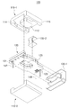
도 1은 본 발명의 제1 실시 예에 따른 성능 개선을 위한 절연 구조가 적용된 평면 트랜스포머를 나타낸 사시도이다.
도 2는 본 발명의 제1 실시 예에 따른 성능 개선을 위한 절연 구조가 적용된 평면 트랜스포머를 상측에서 바라본 분해 사시도이다.
도 3은 본 발명의 제1 실시 예에 따른 성능 개선을 위한 절연 구조가 적용된 평면 트랜스포머를 하측에서 바라본 분해 사시도이다.
도 4는 본 발명의 제1 실시 예에 따른 절연 블록 및 절연 베이스의 결합 방식을 나타낸 사시도이다.
도 5는 본 발명의 제1 실시 예에 따른 절연 블록과 하부 코어의 결합 방식을 나타낸 사시도이다.
도 6은 본 발명의 제1 실시 예에 따른 한 쌍의 페라이트 코어와 2차측 비아홀 간의 최단 절연 거리를 설명하기 위한 평단면도이다.
도 7은 본 발명의 제2 실시 예에 따른 성능 개선을 위한 절연 구조가 적용된 평면 트랜스포머를 나타낸 사시도이다.
도 8은 본 발명의 제2 실시 예에 따른 성능 개선을 위한 절연 구조가 적용된 평면 트랜스포머를 상측에서 바라본 분해 사시도이다.
도 9는 본 발명의 제2 실시 예에 따른 성능 개선을 위한 절연 구조가 적용된 평면 트랜스포머를 하측에서 바라본 분해 사시도이다.
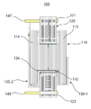
도 10은 본 발명의 제2 실시 예에 따른 트랜스포머의 상면도이다.
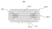
도 11은 본 발명의 제2 실시 예에 따른 트랜스포머의 평단면도이다.
도 12는 도 10에 도시된 트랜스포머를 A-A'라인을 따라 절단한 단면도이다.
도 13은 도 10에 도시된 트랜스포머를 B-B'라인을 따라 절단한 단면도이다.
도 14는 종래 및 본 발명의 제1 실시 예에 따른 트랜스포머에서 구조에 따른 절연 거리를 비교한 평단면도이다.
도 15는 종래 및 본 발명의 제1 실시 예에 따른 트랜스포머에서 2차측 코일 패턴의 크기를 예시적으로 비교한 도면이다.
도 16은 종래 및 본 발명의 제1 실시 예에 따른 트랜스포머에서 동일 원판에서 획득할 수 있는 인쇄회로기판의 수를 비교한 도면이다.
도 17은 종래 및 본 발명의 제1 실시 예에 따른 트랜스포머에서 2차측 코일 패턴의 전기 저항 값을 설명하기 위한 도면이다.1 is a perspective view showing a planar transformer with an insulating structure for improving performance according to a first embodiment of the present invention.
2 is an exploded perspective view of a planar transformer with an insulating structure applied for improving performance according to a first embodiment of the present invention as viewed from above.
3 is an exploded perspective view of a planar transformer applied with an insulating structure for improving performance according to a first embodiment of the present invention as viewed from below.
4 is a perspective view showing a coupling method of an insulating block and an insulating base according to a first embodiment of the present invention.
5 is a perspective view showing a coupling method of an insulating block and a lower core according to a first embodiment of the present invention.
6 is a cross-sectional plan view illustrating a shortest insulation distance between a pair of ferrite cores and a secondary via hole according to a first embodiment of the present invention.
7 is a perspective view showing a planar transformer with an insulating structure for improving performance according to a second embodiment of the present invention.
8 is an exploded perspective view of a planar transformer with an insulating structure for improving performance according to a second embodiment of the present invention as viewed from above.
9 is an exploded perspective view of a planar transformer applied with an insulating structure for improving performance according to a second embodiment of the present invention as viewed from below.
10 is a top view of a transformer according to a second embodiment of the present invention.
11 is a plan cross-sectional view of a transformer according to a second embodiment of the present invention.
12 is a cross-sectional view of the transformer shown in FIG. 10 taken along line A-A '.
13 is a cross-sectional view of the transformer shown in FIG. 10 taken along line B-B '.
14 is a plan cross-sectional view comparing insulation distances according to structures in a transformer according to a first embodiment of the present invention and the present invention.
15 is a view comparing the size of the secondary coil pattern in the transformer according to the first embodiment of the prior art and the present invention by way of example.
16 is a view comparing the number of printed circuit boards that can be obtained from the same original plate in the transformer according to the first embodiment of the prior art and the present invention.
17 is a view for explaining the electrical resistance value of the secondary coil pattern in the transformer according to the first embodiment of the present invention and the prior art.
이하, 첨부된 도면을 참조하여 본 발명의 바람직한 실시 예를 상세히 설명한다. 본 발명의 이점 및 특징, 그리고 그것들을 달성하는 방법은 첨부되는 도면과 함께 상세하게 후술되어 있는 실시 예들을 참조하면 명확해질 것이다. 그러나 본 발명은 이하에서 게시되는 실시 예에 한정되는 것이 아니라 서로 다른 다양한 형태로 구현될 수 있으며, 단지 본 실시 예들은 본 발명의 게시가 완전하도록 하고, 본 발명이 속하는 기술 분야에서 통상의 지식을 가진 자에게 발명의 범주를 완전하게 알려주기 위해 제공되는 것이며, 본 발명은 청구항의 범주에 의해 정의될 뿐이다. 명세서 전체에 걸쳐 동일 참조 부호는 동일 구성 요소를 지칭한다.Hereinafter, preferred embodiments of the present invention will be described in detail with reference to the accompanying drawings. Advantages and features of the present invention, and methods for achieving them will be clarified with reference to embodiments described below in detail together with the accompanying drawings. However, the present invention is not limited to the embodiments disclosed below, but may be implemented in various different forms, and only the embodiments allow the publication of the present invention to be complete, and general knowledge in the technical field to which the present invention pertains. It is provided to fully inform the holder of the scope of the invention, and the invention is only defined by the scope of the claims. The same reference numerals refer to the same components throughout the specification.
다른 정의가 없다면, 본 명세서에서 사용되는 모든 용어(기술 및 과학적 용어를 포함)는 본 발명이 속하는 기술 분야에서 통상의 지식을 가진 자에게 공통적으로 이해될 수 있는 의미로 사용될 수 있을 것이다. 또 일반적으로 사용되는 사전에 정의되어 있는 용어들은 명백하게 특별히 정의되어 있지 않는 한 이상적으로 또는 과도하게 해석되지 않는다. 본 명세서에서 사용된 용어는 실시 예들을 설명하기 위한 것이며 본 발명을 제한하고자 하는 것은 아니다. 본 명세서에서, 단수형은 문구에서 특별히 언급하지 않는 한 복수형도 포함한다.Unless otherwise defined, all terms (including technical and scientific terms) used in the present specification may be used as meanings commonly understood by those skilled in the art to which the present invention pertains. In addition, terms defined in the commonly used dictionary are not ideally or excessively interpreted unless specifically defined. The terminology used herein is for describing the embodiments and is not intended to limit the present invention. In this specification, the singular form also includes the plural form unless otherwise specified in the phrase.
본 명세서에서 사용되는 "포함한다 (comprises)" 및/또는 "포함하는 (comprising)"은 언급된 구성 요소, 단계, 동작 및/또는 소자는 하나 이상의 다른 구성 요소, 단계, 동작 및/또는 소자의 존재 또는 추가를 배제하지 않는다.As used herein, “comprises” and / or “comprising” refers to the components, steps, operations, and / or elements mentioned above of one or more other components, steps, operations, and / or elements. Presence or addition is not excluded.
이하, 본 발명에 대하여 첨부된 도면에 따라 상세히 설명한다.Hereinafter, the present invention will be described in detail according to the accompanying drawings.
도 1은 본 발명의 제1 실시 예에 따른 성능 개선을 위한 절연 구조가 적용된 평면 트랜스포머(100)를 나타낸 사시도이고, 도 2는 본 발명의 제1 실시 예에 따른 성능 개선을 위한 절연 구조가 적용된 평면 트랜스포머(100)를 상측에서 바라본 분해 사시도이며, 도 3은 본 발명의 제1 실시 예에 따른 성능 개선을 위한 절연 구조가 적용된 평면 트랜스포머(100)를 하측에서 바라본 분해 사시도이다.1 is a perspective view showing a
도 1 내지 도 3을 참조하면, 본 발명의 성능 개선을 위한 절연 구조가 적용된 평면 트랜스포머(100)(이하, 트랜스포머라 함)는 서로 전자기 결합되는 상부 코어(110-1) 및 하부 코어(110-2)를 포함하는 한 쌍의 페라이트 코어(110), 한 쌍의 페라이트 코어(110)가 형성한 내부 공간에 배치되는 인쇄회로기판(120)과 이들 간의 절연 거리를 확보하는 절연 블록(130-1) 및 절연 베이스(130-2)를 포함하는 것을 확인할 수 있다.1 to 3, the
먼저, 한 쌍의 페라이트 코어(110)는 트랜스포머(100)를 통해 입력되는 전압이 승압 또는 강압될 수 있는 변환 공정이 이루어지는 내부 공간을 형성할 수 있다. 이를 위해, 한 쌍의 페라이트 코어(110)는 수직 절단면으로 보았을 때, 상부 코어(110-1) 및 하부 코어(110-2)가 눕혀진 E자 형상을 가질 수 있도록 각각 제1 외족(114), 중족(112) 및 제2 외족(115)으로 이루어질 수 있으며, 인쇄회로기판(120)의 일부 영역이 노출될 수 있도록 전후 방향이 개구될 수 있다. 다만, 상부 코어(110-1) 및 하부 코어(110-2)의 형상은 이에 한정되지 않는 다양한 형상이 가능할 수 있다. 예를 들어, 상부 코어(110-1) 및 하부 코어(110-2)는 각각 그 단면이 E-I형, I-I형을 가질 수 있다.First, the pair of
참고로, 본 발명에서 전후 방향이란 도 1의 트랜스포머(100)를 기준으로 보았을 때 절연 블록(130-1)이 배치되지 않은 일측이 전방, 절연 블록(130-1)이 배치된 일측이 후방인 것으로 이해될 수 있다.For reference, in the present invention, the front-rear direction is one side in which the insulating block 130-1 is not disposed, and one side in which the insulating block 130-1 is disposed is rearward when viewed based on the
한편, 한 쌍의 페라이트 코어(110)는 서로 전자기 결합 될 수 있도록 페라이트(Ferrite) 소재로 이루어질 수 있다. 이와 같이, 트랜스포머(100)의 코어가 페라이트 소재로 이루어짐으로써, 한 쌍의 페라이트 코어(110)는 전원 회로의 스위칭 주파수에 따른 자성체 특성을 수백 kHz 이내에서 사용할 수 있으며, 사용 가능한 주파수 대가 높아, 전력 변환이 가능한 용량에 비해 트랜스포머(100)의 소형화가 가능하여 그 무게가 가벼워질 수 있다. 또한, 전력 손실률이 낮아 고주파 대역에서 와전류 손실을 감소시킬 수 있다.Meanwhile, the pair of
다음으로, 인쇄회로기판(120)은 전압을 승압 또는 강압시키는 1차측 코일 패턴과 2차측 코일 패턴을 포함할 수 있다. 구체적으로, 인쇄회로기판(120)의 일단에 마련된 1차측 비아홀(121)로 인입된 전류에 의해 1차측 코일 패턴에서 발생한 유도 기전력이 2차측 코일 패턴으로 유도되어 인쇄회로기판(120)의 타단에 마련된 2차측 비아홀(123)로 출력될 수 있다.Next, the printed
이와 같이, 1차측 비아홀(121) 및 2차측 비아홀(123)로 전압이 입, 출력 되기 위해, 인쇄회로기판(120)은 1차측 비아홀(121)이 마련된 일단에서 1차측 비아홀(121)과 전기적으로 결선되는 제1 리드핀(147)이 구비되고, 2차측 비아홀(123)이 마련된 타단에서 2차측 비아홀(123)과 전기적으로 결선되는 제2 리드핀(149)이 구비될 수 있다.As described above, in order for voltage to be input and output to the primary side via
아울러, 인쇄회로기판(120)은 한 쌍의 페라이트 코어(110) 내에 배치되는 바, 인쇄회로기판(120)의 내부에는 한 쌍의 페라이트 코어(110)의 중족(112)이 삽입될 수 있는 삽입 홀(125)이 형성될 수 있다. In addition, the printed
한편, 본 발명에서 인쇄회로기판(120)이 하나인 것으로 도시되었으나, 코일 패턴을 포함하는 적어도 두 개 이상의 인쇄회로기판(120)이 적층될 수 있다.Meanwhile, in the present invention, although the printed
마지막으로, 절연 블록(130-1) 및 절연 베이스(130-2)는 트랜스포머(100)의 전기적 안정성을 위해, 한 쌍의 페라이트 코어(110) 및 인쇄회로기판(120)과 결합함으로써 한 쌍의 페라이트 코어(110)와 2차측 비아홀(123) 간의 절연 거리를 확보할 수 있다. 여기서, 절연 거리란 1차측 부품인 한 쌍의 페라이트 코어(110)의 노출지점으로부터 2차측 부품인 2차측 비아홀(123)까지의 가장 짧은 거리이며, 절연면을 따라 측정한 거리가 규격 절연 거리보다 길어야 한다.Finally, the insulating block 130-1 and the insulating base 130-2 are paired by combining with a pair of
구체적으로, 절연 블록(130-1)은 한 쌍의 페라이트 코어(110)의 일측을 수용할 수 있으며, 절연 베이스(130-2)는 디귿자 형상을 이루며 한 쌍의 페라이트 코어(110) 내에 배치될 수 있다. 또한, 조립 과정에서 절연 블록(130-1)과 끼움 결합될 수 있다. 즉, 절연 블록(130-1) 및 절연 베이스(130-2)는 2차측 비아홀(123)이 마련된 인쇄회로기판(120)의 일부 영역을 감싸듯이 수용할 수 있으며, 이를 통해 한 쌍의 페라이트 코어(110)의 노출지점을 2차측 비아홀(123)과 멀어지게 함으로써, 상대적으로 길이가 짧은 인쇄회로기판(120) 내에서도 1차측 부품과 2차측 부품 간의 규격 절연 거리를 확보할 수 있어, 규격 거리를 확보하기 위해 인쇄회로기판(120)에 형성된 코일 패턴의 길이를 증가시키지 않을 수 있다. Specifically, the insulating block 130-1 may accommodate one side of the pair of
지금까지 본 발명의 제1 실시 따른 트랜스포머(100)가 포함하는 구성 요소에 대하여 개략적으로 설명하였으며, 이하에서는 트랜스포머(100) 내 1차측 부품과 2차측 부품 간의 규격된 절연 거리를 확보할 수 있는 절연 블록(130-1) 및 절연 베이스(130-2)에 대한 구체적인 형상에 대하여 설명하도록 한다.So far, the components included in the
도 4는 본 발명의 제1 실시 예에 따른 절연 블록(130-1) 및 절연 베이스(130-2)의 결합 방식을 나타낸 사시도이고, 도 5는 본 발명의 제1 실시 예에 따른 절연 블록(130-1)과 하부 코어(110-2)의 결합 방식을 나타낸 사시도이며, 도 6은 본 발명의 제1 실시 예에 따른 한 쌍의 페라이트 코어(110)와 2차측 비아홀(123) 간의 최단 절연 거리를 설명하기 위한 평단면도이다.4 is a perspective view showing a coupling method of the insulating block 130-1 and the insulating base 130-2 according to the first embodiment of the present invention, and FIG. 5 is an insulating block according to the first embodiment of the present invention ( 130-1) is a perspective view showing a coupling method of the lower core 110-2, and FIG. 6 is the shortest insulation between the pair of
도 4의 (a) 및 (b)를 참조하면, 절연 블록(130-1)과 절연 베이스(130-2)는 서로 교차 결합되는 형상으로 이루어질 수 있으며, 교차 결합된 공간에서 인쇄회로기판(120)의 일부 영역을 수용할 수 있다. 구체적으로, 절연 베이스(130-2)는 한 쌍의 페라이트 코어(110)의 중족(112) 또는 인쇄회로기판(120)의 삽입 홀(125)이 형성된 일면과 맞닿는 제1 베이스 절연면(135)과 제1 베이스 절연면(135)에서부터 연장되며 각각 인쇄회로기판(120)의 상면 및 하면과 맞닿는 제2 베이스 절연면(136)을 포함할 수 있다. 즉, 절연 베이스(130-2)는 디귿자 형상을 가지고 한 쌍의 페라이트 코어(110)의 중족(112)과 인쇄회로기판(120)이 맞닿는 일면에 배치됨으로써 절연 거리를 확보할 수 있다.Referring to (a) and (b) of FIG. 4, the insulating block 130-1 and the insulating base 130-2 may be formed to be cross-coupled with each other, and the printed
한편, 절연 블록(130-1)은 한 쌍의 페라이트 코어(110)의 일측에 삽입되며, 제2 베이스 절연면(136)과 끼움 결합되는 제1 블록 절연면(137)을 포함할 수 있는데, 이 때 제1 블록 절연면(137)은 제2 베이스 절연면(136), 즉 절연 베이스(130-2)와 견고하게 결합될 수 있도록 소정의 홈(137-1)이 마련될 수 있다.Meanwhile, the insulating block 130-1 is inserted into one side of the pair of
즉, 도 5의 (a)와 같이, 절연 블록(130-1)의 제1 블록 절연면(137)에는 홈(137-1)이 마련될 수 있으며, 절연 블록(130-1)은 상부 코어(110-1) 및 하부 코어(110-2)의 노출면의 일부를 수용할 수 있는 제2 블록 절연면(138)을 포함함으로써, 별도의 접착 부재(예. 접착제, 테이프) 없이도 절연 베이스(130-2)와 견고히 결합되고 절연 거리를 확보할 수 있다.That is, as shown in (a) of FIG. 5, a groove 137-1 may be provided on the first
아울러, 도 5의 (b)를 참조하면, 결합된 형상을 수직 절단면으로 보았을 때, 서로 견고하게 결합된 절연 블록(130-1) 및 절연 베이스(130-2)가 하부 코어(110-2)에 안착되기 위해, 하부 코어(110-2)의 내측면에서 절연 수용면(116)이 마련될 수 있다. 구체적으로, 하부 코어(110-2)는 절연 수용면(116)이 마련된 영역에서 보다 얇은 두께를 가짐으로써, 절연 블록(130-1)이 하부 코어(110-2)를 보다 용이하게 수용할 수 있다. In addition, referring to (b) of FIG. 5, when the combined shape is viewed as a vertical cut surface, the insulation block 130-1 and the insulation base 130-2 that are firmly coupled to each other are the lower core 110-2. In order to be seated therein, an insulating
한편, 도 5의 (b)는 하부 코어(110-2)를 기준으로 설명하였으나, 상부 코어(110-1)에도 마찬가지로 그 내부면에 절연 블록(130-1)을 수용하기 위한 절연 수용면(116)이 마련될 수 있다.On the other hand, (b) of FIG. 5 has been described with reference to the lower core 110-2, but the upper core 110-1 has an insulating receiving surface for accommodating the insulating block 130-1 on its inner surface. 116) may be provided.
또한, 도 5의 (c)를 참조하면, 결합된 형상을 후방에서 바라보았을 때, 절연 블록(130-1)은 제1 블록 절연면(137)과 제2 블록 절연면(138)을 연결하는 제3 블록 절연면(139)을 더 포함할 수 있다. 이러한 제3 블록 절연면(139)은 2차측 비아홀(123)이 마련된 인쇄회로기판(120)을 한 쌍의 페라이트 코어(110)의 외부로 노출시키기 위한 홀(139-1)이 마련되어, 절연 블록(130-1)이 삽입하는 것만으로도 한 쌍의 페라이트 코어(110)를 안정적으로 고정시킬 수 있다.In addition, referring to (c) of FIG. 5, when the combined shape is viewed from the rear, the insulating block 130-1 connects the first
도 6을 참조하면, 한 쌍의 페라이트 코어(110) 사이에 인쇄회로기판(120)이 배치되어 있으며, 한 쌍의 페라이트 코어(110)는 제1 외족(114), 중족(112) 및 제2 외족(115)이 서로 전자기 결합되어 마그네틱 플럭스(magnetic flux)의 이동 경로를 제공할 수 있다. 여기서, 중족(112)은 인쇄회로기판(120)의 삽입 홀(125)에 삽입되어, 1차측과 2차측의 마그네틱 플럭스를 중계하는 경로를 형성할 수 있다. 즉, 1차측 비아홀(121)에 인가된 입력 전류가 인쇄회로기판(120) 내 1차측 코일 패턴에 의해 기전력을 발생시키고, 그 기전력이 인쇄회로기판(120) 내 2차측 코일 패턴으로 유기되어 2차측 비아홀(123)로 출력될 수 있다.Referring to FIG. 6, a printed
이러한 트랜스포머(100)의 성능을 유지함과 동시에 소형화를 구현하기 위해, 한 쌍의 페라이트 코어(110) 내부에 절연 베이스(130-2)를, 한 쌍의 페라이트 코어(110) 외부에 절연 블록(130-1)을 배치시키며, 각각이 마주보는 디귿자 형상을 가짐으로써 서로 견고하게 끼움 결합될 수 있다.In order to maintain the performance of the
한편, 절연 블록(130-1) 및 절연 베이스(130-2)가 배치되어, 중족(112)의 일부를 절연함으로써, 절연 수단의 우회 길이를 통해 절연 거리가 확보되므로, 상부 코어(110-1) 및 하부 코어(110-2)의 중족(112) 외측면으로부터 2차측 비아홀(123)까지 최단 절연 거리(t)가 7mm 보다 더 짧은 직선 거리로 구현될 수 있어, 종래에 비해 인쇄회로기판(120)의 크기가 상대적으로 작아질 수 있다.On the other hand, since the insulating block 130-1 and the insulating base 130-2 are arranged, by insulating a part of the
지금까지 본 발명의 제1 실시 예에 따른 트랜스포머(100)에 대하여 설명하였다. 본 발명에 따르면, 한 쌍의 페라이트 코어(110)와 2차측 비아홀(123) 사이에 확보되어야 할 절연 거리(t)를 인쇄회로기판(120)의 일부 영역을 감싸는 구조를 가지는 절연 블록(130-1) 및 절연 베이스(130-2)를 통해 확보함으로써, 인쇄회로기판(120)에 형성되는 코일 패턴의 길이를 최소화할 수 있고, 그에 따라 트랜스포머(100)의 전체 크기가 소형화되고 그 성능이 개선될 수 있다.So far, the
이하에서는 절연 거리를 확보할 수 있는 또 다른 구조의 트랜스포머(100)에 대하여 설명하도록 한다.Hereinafter, a
도 7은 본 발명의 제2 실시 예에 따른 성능 개선을 위한 절연 구조가 적용된 평면 트랜스포머(100)를 나타낸 사시도이고, 도 8은 본 발명의 제2 실시 예에 따른 성능 개선을 위한 절연 구조가 적용된 평면 트랜스포머(100)를 상측에서 바라본 분해 사시도이며, 도 9는 본 발명의 제2 실시 예에 따른 성능 개선을 위한 절연 구조가 적용된 평면 트랜스포머(100)를 하측에서 바라본 분해 사시도이다.7 is a perspective view showing a
도 7 내지 도 9를 참조하면, 본 발명의 제2 실시 예에 따른 트랜스포머(100)는 서로 전자기 결합되는 상부 코어(110-1) 및 하부 코어(110-2)를 포함하는 한 쌍의 페라이트 코어(110), 한 쌍의 페라이트 코어(110)가 형성한 내부 공간에 배치되는 인쇄회로기판(120)과 이를 절연시키는 절연 블록(130-1) 및 절연 베이스(130-2)를 포함하는 것을 확인할 수 있다.7 to 9, the
먼저, 한 쌍의 페라이트 코어(110)는 트랜스포머(100)를 통해 입력되는 전압이 승압 또는 강압될 수 있는 변환 공정이 이루어지는 내부 공간을 형성할 수 있다. 이를 위해, 한 쌍의 페라이트 코어(110)는 수직 절단면으로 보았을 때, 상부 코어(110-1) 및 하부 코어(110-2)가 눕혀진 E자 형상을 가질 수 있도록 각각 제1 외족(114), 중족(112) 및 제2 외족(115)으로 이루어질 수 있으며, 인쇄회로기판(120)의 일부 영역이 노출될 수 있도록 전후 방향이 개구될 수 있다. 다만, 상부 코어(110-1) 및 하부 코어(110-2)의 형상은 이에 한정되지 않는 다양한 형상이 가능할 수 있다. 예를 들어, 상부 코어(110-1) 및 하부 코어(110-2)는 각각 그 단면이 E-I형, I-I형을 가질 수 있다.First, the pair of
한편, 한 쌍의 페라이트 코어(110)는 서로 전자기 결합 될 수 있도록 페라이트(Ferrite) 소재로 이루어질 수 있다. 이와 같이, 트랜스포머(100)의 코어가 페라이트 소재로 이루어짐으로써, 한 쌍의 페라이트 코어(110)는 전원 회로의 스위칭 주파수에 따른 자성체 특성을 수백 kHz 이내에서 사용할 수 있으며, 사용 가능한 주파수 대가 높아, 전력 변환이 가능한 용량에 비해 트랜스포머(100)의 소형화가 가능하여 그 무게가 가벼워질 수 있다. 또한, 전력 손실률이 낮아 고주파 대역에서 와전류 손실을 감소시킬 수 있다.Meanwhile, the pair of
다음으로, 인쇄회로기판(120)은 전압을 승압 또는 강압시키는 1차측 코일 패턴과 2차측 코일 패턴을 포함할 수 있다. 구체적으로, 인쇄회로기판(120)의 일단에 마련된 1차측 비아홀(121)로 인입된 전류에 의해 1차측 코일 패턴에서 발생한 유도 기전력이 2차측 코일 패턴으로 유도되어 인쇄회로기판(120)의 타단에 마련된 2차측 비아홀(123)로 출력될 수 있다.Next, the printed
이와 같이, 1차측 비아홀(121) 및 2차측 비아홀(123)로 전압이 입, 출력 되기 위해, 인쇄회로기판(120)은 1차측 비아홀(121)이 마련된 일단에서 1차측 비아홀(121)과 전기적으로 결선되는 제1 리드핀(147)이 구비되고, 2차측 비아홀(123)이 마련된 타단에서 2차측 비아홀(123)과 전기적으로 결선되는 제2 리드핀(149)이 구비될 수 있다.As described above, in order for voltage to be input and output to the primary side via
아울러, 인쇄회로기판(120)은 한 쌍의 페라이트 코어(110) 내에 배치되는 바, 인쇄회로기판(120)의 내부에는 한 쌍의 페라이트 코어(110)의 중족(112)이 삽입될 수 있는 삽입 홀(125)이 형성될 수 있다. In addition, the printed
한편, 본 발명에서 인쇄회로기판(120)이 하나인 것으로 도시되었으나, 코일 패턴을 포함하는 적어도 두 개 이상의 인쇄회로기판(120)이 적층될 수 있다.Meanwhile, in the present invention, although the printed
마지막으로, 절연 블록(130-1) 및 절연 베이스(130-2)는 전기적 안정성을 위해, 한 쌍의 페라이트 코어(110)와 2차측 비아홀(123) 간의 절연 거리를 확보할 수 있다. 여기서, 절연 거리란 1차측 부품인 한 쌍의 페라이트 코어(110)의 노출지점으로부터 2차측 부품인 2차측 비아홀(123)까지의 가장 짧은 거리이며, 절연면을 따라 측정한 거리가 규격 절연 거리보다 길어야 한다.Finally, the insulating block 130-1 and the insulating base 130-2 may secure an insulating distance between the pair of
구체적으로, 절연 블록(130-1)과 절연 베이스(130-2)는 서로 교차 결합되는 형상으로 이루어지며, 절연 블록(130-1)은 상부 코어 측면(111)을 수용하며 절연 거리를 확보하는 블록 외부 절연면(131)과 상부 코어(110-1)의 중족(112) 일부를 수용하며 절연 거리를 확보하는 블록 내부 절연면(132)을 포함하고, 절연 베이스(130-2)는 하부 코어 측면(113)을 수용하며 절연 거리를 확보하는 베이스 외부 절연면(133)과 하부 코어(110-2)의 중족(112) 일부를 수용하며 절연 거리를 확보하는 베이스 내부 절연면(134)을 포함할 수 있다.Specifically, the insulating block 130-1 and the insulating base 130-2 are formed to be cross-coupled with each other, and the insulating block 130-1 accommodates the
아울러, 절연 블록(130-1)과 절연 베이스(130-2)의 블록 외부 절연면(131) 및 베이스 외부 절연면(133)은 각각 인쇄회로기판(120)의 2차측 비아홀(123)에 대하여 이격되게 마련될 수 있다.In addition, the insulating block 130-1 and the insulating
또한, 절연 베이스(130-2)는 한 쌍의 페라이트 코어(110)와 절연 블록(130-1)을 수용하는 구조로 이루어질 수 있는데, 절연 베이스(130-2)는 그 내측에 하부 코어(110-2)를 수용하며, 그 위에 상부 코어(110-1)가 수용된 절연 블록(130-1)이 안착될 수 있다. 즉, 블록 외부 절연면(131)과 베이스 외부 절연면(133)이, 블록 내부 절연면(132)과 베이스 내부 절연면(134)이 서로 교차 결합되어 매우 견고한 트랜스포머 구조를 이룰 수 있다.In addition, the insulating base 130-2 may be formed of a structure that accommodates a pair of
지금까지 본 발명의 제2 실시 예에 따른 트랜스포머(100)가 포함하는 구성에 대하여 개략적으로 설명하였다. 본 발명에 따르면, 트랜스포머(100)는 한 쌍의 페라이트 모어(110)와 2차측 비아홀(123) 사이에 확보되어야 하는 규격 절연 거리(t)를, 상술한 바와 같이 서로 삽입되는 특별한 구조의 절연 블록(130-1)과 절연 베이스(130-2)를 트랜스포머(100) 내에 별도로 마련함으로써, 인쇄회로기판(120)에 형성된 코일 패턴의 길이를 최소화할 수 있으며, 트랜스포머(100)의 소형화 및 성능 개선이 가능할 수 있다.So far, the configuration included in the
이하에서는 절연 거리를 확보할 수 있는 절연 블록(130-1) 및 절연 베이스(130-2)의 구조에 대해 보다 구체적으로 설명하도록 한다.Hereinafter, structures of the insulating block 130-1 and the insulating base 130-2 that can secure the insulating distance will be described in more detail.
도 10은 본 발명의 제2 실시 예에 따른 트랜스포머(100)의 상면도이고, 도 11은 본 발명의 제2 실시 예에 따른 트랜스포머(100)의 평단면도이며, 도 12는 도 10에 도시된 트랜스포머(100)를 A-A'라인을 따라 절단한 단면도이며, 도 13은 도 10에 도시된 트랜스포머(100)를 B-B'라인을 따라 절단한 단면도이다.FIG. 10 is a top view of the
도 10 내지 도 13을 참조하면, 트랜스포머(100)는 한 쌍의 페라이트 코어(110) 사이에 인쇄회로기판(120)이 배치되어 있으며, 한 쌍의 페라이트 코어(110)는 제1 외족(114), 중족(112) 및 제2 외족(115)이 서로 전자기 결합되어 마그네틱 플럭스(magnetic flux)의 이동 경로를 제공할 수 있다. 여기서, 중족(112)은 인쇄회로기판(120)의 삽입 홀(125)에 삽입되어, 1차측과 2차측의 마그네틱 플럭스를 중계하는 경로를 형성할 수 있다. 즉, 1차측 비아홀(121)에 인가된 입력 전류가 인쇄회로기판(120)내 1차측 코일 패턴에 의해 기전력을 발생시키고, 그 기전력이 인쇄회로기판(120) 내 2차측 코일 패턴으로 유기되어 2차측 비아홀(123)로 출력될 수 있다.10 to 13, the
이러한 트랜스포머(100)의 성능을 유지함과 동시에 소형화를 구현하기 위해, 상부 코어(110-1)와 결합된 절연 블록(130-1)과 하부 코어(110-2)와 결합된 절연 베이스(130-2)를 인쇄회로기판(120)에 결합할 수 있다. 즉, 상부 코어(110-1)와 결합된 절연 블록(130-1)과 하부 코어(110-2)와 결합된 절연 베이스(130-2)를 인쇄회로기판(120)의 삽입 홀(125)에 삽입하여 서로 결합시킬 수 있으며, 이 과정에서 인쇄회로기판(120)을 감싸고 있는 한 쌍의 페라이트 코어(110)는 절연 블록(130-1)과 절연 베이스(130-2)를 통해 인쇄회로기판(120)과 절연 구조로 안착될 수 있다. In order to maintain the performance of the
또한, 하부 코어(110-2)와 결합된 절연 베이스(130-2)는 그 내측에 상부 코어(110-1)와 결합된 절연 블록(130-1)이 안착되며, 블록 외부 절연면(131)과 베이스 외부 절연면(133)이, 블록 내부 절연면(132)과 베이스 내부 절연면(134)이 서로 교차 결합하여, 외력에도 흔들림이 없는 견고한 구조를 가질 수 있다.In addition, the insulating base 130-2 coupled with the lower core 110-2 is seated with an insulating block 130-1 coupled with the upper core 110-1 on its inner side, and an outer insulating
이하에서는 도면을 참조하여 종래 트랜스포머의 구조와 본 발명의 제1 실시 예에 따른 트랜스포머의 구조를 비교하도록 한다.Hereinafter, a structure of a conventional transformer and a structure of a transformer according to the first embodiment of the present invention will be compared with reference to the drawings.
도 14는 종래 및 본 발명의 제1 실시 예에 따른 트랜스포머(100)에서 구조에 따른 절연 거리를 비교한 평단면도이다.14 is a plan cross-sectional view comparing insulation distances according to structures in the
도 14의 (1)은 종래의 절연 구조를 나타낸 것으로서, 종래에는 상부 코어(210-1) 및 하부 코어(210-2)의 중족(212)과 2차측 비아홀(223) 사이에 어떠한 절연 부재도 존재하지 않아, 중족(212)과 2차측 비아홀(223) 간의 최단 절연 거리(t)가 직선 거리로 최소 7mm 이상이 될 수 밖에 없었다.14 (1) shows a conventional insulating structure, and conventionally, any insulating member between the middle 212 and the secondary via
반면, 도 14의 (2)는 본 발명의 트랜스포머(100) 구조로서, 절연 블록(130-1) 및 절연 베이스(130-2)를 통해 중족(112)의 일부를 절연함으로써, 절연 수단의 우회 길이를 통해 절연 거리가 확보되므로, 중족(112)과 2차측 비아홀(123)과의 최단 절연 거리(t)가 7mm 보다 더 짧은 직선 거리로 구현할 수 있다. 즉, 종래에 비해 인쇄회로기판(120)의 크기가 상대적으로 작아질 수 있다.On the other hand, Fig. 14 (2) is a
도 15는 종래 및 본 발명의 제1 실시 예에 따른 트랜스포머(100)에서 2차측 코일 패턴의 크기를 예시적으로 비교한 도면이다.15 is a view comparing the size of the secondary coil pattern in the
도 15의 (1)은 종래 트랜스포머(200)에서 인쇄회로기판(220) 내에 형성된 2차측 코일 패턴(250)의 형상, 도 15의 (2)는 본 발명의 트랜스포머(100)에서 인쇄회로기판(120) 내에 형성된 2차측 코일 패턴(150)의 형상을 나타낸 것으로써, 종래에 비해 본 발명에서 2차측 코일 패턴(150)의 크기가 좀 더 작아지는 것을 알 수 있으며, 이를 통해 트랜스포머(100)가 보다 소형화될 수 있음을 알 수 있다.15 (1) shows the shape of the
또한, 이와 관련하여, 도 16은 종래 및 본 발명의 제1 실시 예에 따른 트랜스포머(100)에서 동일 원판에서 획득할 수 있는 인쇄회로기판의 수를 비교한 도면으로서, 도 16을 참조하면, 일반적으로 다층 인쇄회로기판의 제조에 사용되는 원판의 크기가 1000x1000mm 인 바, 도 16의 (1)과 같이 종래의 트랜스포머에 사용되는 인쇄회로기판은 하나의 원판에서 약 2,009개의 인쇄회로기판(19.15x22.8mm)을 생산할 수 있지만, 도 16의 (2)와 같이 본 발명의 트랜스포머에 사용되는 인쇄회로기판은 하나의 원판에서 약 2,205개의 인쇄회로기판(19.15x21.0mm)을 생산할 수 있다.In addition, in this connection, FIG. 16 is a diagram comparing the number of printed circuit boards that can be obtained from the same original plate in the
즉, 하나의 동일한 원판으로 196개의 인쇄회로기판을 더 생산할 수 있어, 약 10% 정도로 원가를 절감할 수 있어, 보다 경제적일 수 있다.That is, since 196 printed circuit boards can be further produced from one and the same disk, the cost can be reduced by about 10%, and thus it can be more economical.
도 17은 종래 및 본 발명의 제1 실시 예에 따른 트랜스포머(100)에서 2차측 코일 패턴의 전기 저항 값을 설명하기 위한 도면이다.17 is a view for explaining the electrical resistance value of the secondary coil pattern in the
도 17의 (1)을 참조하면, 종래의 트랜스포머는 충전기 회로의 스위칭 주파수가 100kHz이고, 출력 전압 및 출력 전류가 5V/3A이며, 전류 밀도(251)에 따른 인쇄회로기판의 온도가 다음과 같을 때, 교류 전기저항 성분은 42.1(m옴)이 되며, 2차측 출력 전력이 15W일 때, 전기저항 42.1(m옴)으로 인한 전력 손실은 378.9mW인 것을 확인할 수 있다.17 (1), the conventional transformer has a switching frequency of a charger circuit of 100 kHz, an output voltage and an output current of 5 V / 3 A, and a temperature of the printed circuit board according to the
반면, 도 17의 (2)를 참조하면, 본 발명의 트랜스포머(100)는 충전기 회로의 스위칭 주파수가 100kHz이고, 출력 전압 및 출력 전류가 5V/3A이며 전류 밀도(151)에 따른 인쇄회로기판(200)의 온도가 다음과 같을 때, 교류 전기저항 성분은 31.8(m옴)이 되며, 2차측 출력 전력이 15W일 때, 전기저항 31.8(m옴)으로 인한 전력 손실은 286.2mW인 것을 확인할 수 있어, 전력 손실이 종래에 비해 감소한 것을 알 수 있다.On the other hand, referring to (2) of FIG. 17, the
즉, 본 발명의 트랜스포머(100)는 절연 블록(130-1) 및 절연 베이스(130-2)를 삽입함으로써, 종래에 비해 약 25% 정도 전력 손실을 줄일 수 있다.That is, by inserting the insulating block 130-1 and the insulating base 130-2 of the
한편, 상술한 종래와 본 발명의 비교는 제1 실시 예를 기준으로 설명하였으나, 본 발명의 제2 실시 예에서도 절연 블록(130-1) 및 절연 베이스(130-2)를 배치를 통해 동일한 효과를 얻을 수 있는 것으로 이해될 수 있다.On the other hand, the comparison between the above-described conventional and the present invention has been described based on the first embodiment, but in the second embodiment of the present invention, the same effect is achieved through the arrangement of the insulating block 130-1 and the insulating base 130-2. It can be understood that can be obtained.
이상 첨부된 도면을 참조하여 본 발명의 실시 예들을 설명하였지만, 본 발명이 속하는 기술 분야에서 통상의 지식을 가진 자는 본 발명이 그 기술적 사상이나 필수적인 특징을 변경하지 않고서 다른 구체적인 형태로 실시될 수 있다는 것을 이해할 수 있을 것이다. 그러므로 이상에서 기술한 실시 예들은 모든 면에서 예시적인 것이며 한정적이 아닌 것으로 이해해야만 한다.Although the embodiments of the present invention have been described with reference to the accompanying drawings, a person skilled in the art to which the present invention pertains may be implemented in other specific forms without changing the technical concept or essential features of the present invention. You will understand. Therefore, it should be understood that the embodiments described above are illustrative in all respects and not restrictive.
100: 평면 트랜스포머
110: 페라이트 코어
110-1: 상부 코어
110-2: 하부 코어
111: 상부 코어 측면
113: 하부 코어 측면
112: 중족
114: 제1 외족
115: 제2 외족
116: 절연 수용면
120: 인쇄회로기판
121: 1차측 비아홀
123: 2차측 비아홀
130-1: 절연 블록
130-2: 절연 베이스
131: 블록 외부 절연면
132: 블록 내부 절연면
133: 베이스 외부 절연면
134: 베이스 내부 절연면
135: 제1 베이스 절연면
136: 제2 베이스 절연면
137: 제1 블록 절연면
138: 제2 블록 절연면
139: 제3 블록 절연면
147: 제1 리드핀
149: 제2 리드핀
150: 코일 패턴
151: 전류 밀도100: planar transformer
110: ferrite core
110-1: upper core 110-2: lower core
111: upper core side 113: lower core side
112: midfoot
114: first aliens 115: second aliens
116: insulating receiving surface
120: printed circuit board
121: primary via hole 123: secondary via hole
130-1: Insulation block 130-2: Insulation base
131: insulating surface outside the block 132: insulating surface inside the block
133: base outer insulating surface 134: base inner insulating surface
135: first base insulating surface 136: second base insulating surface
137: first block insulating surface 138: second block insulating surface
139: third block insulation surface
147: first lead pin 149: second lead pin
150: coil pattern 151: current density
Claims (10)
상기 한 쌍의 페라이트 코어(110) 사이에 배치되며, 일단에 1차측 코일 패턴을 전기적으로 연결하는 1차측 비아홀(121)이 마련되고, 타단에 2차측 코일 패턴을 전기적으로 연결하는 2차측 비아홀(123)이 마련된 인쇄회로기판(120);
상기 한 쌍의 페라이트 코어(110)의 일측을 수용하는 절연 블록(130-1); 및
상기 한 쌍의 페라이트 코어(110) 내에 배치되어 상기 절연 블록(130-1)과 끼움 결합되는 절연 베이스(130-2); 를 포함하되,
상기 절연 블록(130-1) 및 상기 절연 베이스(130-2)는,
상기 2차측 비아홀(123)이 마련된 일측에서 상기 인쇄회로기판(120)의 일부 영역을 수용하는 것을 특징으로 하는 성능 개선을 위한 절연 구조가 적용된 평면 트랜스포머.A pair of ferrite cores 110 composed of an upper core 110-1 and a lower core 110-2;
A secondary via hole 121 disposed between the pair of ferrite cores 110 and electrically connecting a primary coil pattern to one end is provided, and a secondary via hole electrically connecting a secondary coil pattern to the other end ( 123) is provided with a printed circuit board 120;
An insulating block 130-1 accommodating one side of the pair of ferrite cores 110; And
An insulating base 130-2 disposed in the pair of ferrite cores 110 and fitted with the insulating block 130-1; Including,
The insulating block (130-1) and the insulating base (130-2),
A planar transformer with an insulating structure for improving performance, characterized in that a portion of the printed circuit board 120 is accommodated at one side where the secondary via hole 123 is provided.
상기 절연 베이스(130-2)는,
상기 한 쌍의 페라이트 코어(110)의 중족(112)과 맞닿는 제1 베이스 절연면(135); 및
상기 제1 베이스 절연면(135)에서부터 연장되며 각각 상기 인쇄회로기판(120)의 상면 및 하면과 맞닿는 제2 베이스 절연면(136); 을 포함하는 것을 특징으로 하는 성능 개선을 위한 절연 구조가 적용된 평면 트랜스포머.According to claim 1,
The insulating base 130-2,
A first base insulating surface 135 in contact with the midfoot 112 of the pair of ferrite cores 110; And
A second base insulating surface 136 extending from the first base insulating surface 135 and contacting the upper and lower surfaces of the printed circuit board 120, respectively; A planar transformer with an insulating structure for improving performance, characterized in that it comprises a.
상기 절연 블록(130-1)은,
상기 한 쌍의 페라이트 코어(110)의 일측에 삽입되며,
상기 제2 베이스 절연면(136)과 끼움 결합되는 제1 블록 절연면(137); 을 더 포함하는 것을 특징으로 하는 성능 개선을 위한 절연 구조가 적용된 평면 트랜스포머.According to claim 2,
The insulating block 130-1,
Is inserted into one side of the pair of ferrite core 110,
A first block insulating surface 137 which is fitted with the second base insulating surface 136; A planar transformer with an insulating structure for improving performance, further comprising a.
상기 절연 블록(130-1)은,
상기 한 쌍의 페라이트 코어(110)의 일측에 삽입되며,
상기 상부 코어(110-1) 및 상기 하부 코어(110-2)의 외부 노출면의 일부를 수용하는 제2 블록 절연면(138); 을 더 포함하는 것을 특징으로 하는 성능 개선을 위한 절연 구조가 적용된 평면 트랜스포머.According to claim 3,
The insulating block 130-1,
Is inserted into one side of the pair of ferrite core 110,
A second block insulating surface 138 accommodating a portion of the outer exposed surfaces of the upper core 110-1 and the lower core 110-2; A planar transformer with an insulating structure for improving performance, further comprising a.
상기 상부 코어(110) 및 상기 하부 코어(110)는 상기 인쇄회로기판(120)이 배치되는 내측면에서,
끼움 결합된 상기 제2 베이스 절연면(136) 및 상기 제1 블록 절연면(137)이 안착되는 절연 수용면(116)이 마련되는 것을 특징으로 하는 성능 개선을 위한 절연 구조가 적용된 평면 트랜스포머.According to claim 3,
The upper core 110 and the lower core 110 are on the inner surface on which the printed circuit board 120 is disposed,
A planar transformer having an insulating structure for improving performance, characterized in that an insulating receiving surface 116 on which the second base insulating surface 136 and the first block insulating surface 137 are fitted is provided.
상기 중족(112)의 외측면으로부터 상기 2차측 비아홀(123)까지의 최단 직선 거리는 7mm 이하인 것을 특징으로 하는 성능 개선을 위한 절연 구조가 적용된 평면 트랜스포머.According to claim 4,
The shortest straight distance from the outer surface of the midfoot 112 to the secondary via hole 123 is 7 mm or less, a planar transformer with an insulating structure for improving performance.
상기 절연 블록(130-1)은,
상기 제1 블록 절연면(137)과 제2 블록 절연면(138)을 연결하는 제3 블록 절연면(139); 을 더 포함하고,
상기 제3 블록 절연면(139)은,
상기 2차측 비아홀(123)이 마련된 상기 인쇄회로기판(120)을 상기 한 쌍의 페라이트 코어(110)의 외부로 노출시키기 위한 홀(H)이 마련되는 것을 특징으로 하는 성능 개선을 위한 절연 구조가 적용된 평면 트랜스포머.According to claim 4,
The insulating block 130-1,
A third block insulating surface 139 connecting the first block insulating surface 137 and the second block insulating surface 138; Further comprising,
The third block insulating surface 139,
An insulating structure for improving performance, characterized in that a hole (H) for exposing the printed circuit board 120 provided with the secondary via hole 123 to the outside of the pair of ferrite cores 110 is provided. Planar transformer applied.
상기 한 쌍의 페라이트 코어(110) 사이에 배치되며, 일단에 1차측 코일 패턴을 전기적으로 연결하는 1차측 비아홀(121)이 마련되고, 타단에 2차측 코일 패턴을 전기적으로 연결하는 2차측 비아홀(123)이 마련된 인쇄회로기판(120);
상기 상부 코어(110-1)의 일부를 수용하는 수용하여 상기 한 쌍의 페라이트 코어(110)와 상기 2차측 비아홀(123) 간의 절연 거리를 확보하는 절연 블록(130-1); 및
상기 하부 코어(110-2)의 일부를 수용하는 수용하여 상기 한 쌍의 페라이트 코어(110)와 상기 2차측 비아홀(123) 간의 절연 거리를 확보하는 절연 베이스(130-2); 를 포함하되,
상기 절연 블록(130-1)과 상기 절연 베이스(130-2)가 결합되어 상기 인쇄회로기판(120)을 수용하는 것을 특징으로 하는 성능 개선을 위한 절연 구조가 적용된 평면 트랜스포머.A pair of ferrite cores 110 composed of an upper core 110-1 and a lower core 110-2;
A secondary via hole 121 disposed between the pair of ferrite cores 110 and electrically connecting a primary coil pattern to one end is provided, and a secondary via hole electrically connecting a secondary coil pattern to the other end ( 123) is provided with a printed circuit board 120;
An insulating block (130-1) accommodating a portion of the upper core (110-1) to secure an insulating distance between the pair of ferrite cores (110) and the secondary via hole (123); And
An insulating base 130-2 accommodating a portion of the lower core 110-2 to secure an insulating distance between the pair of ferrite cores 110 and the secondary via hole 123; Including,
The insulating block (130-1) and the insulating base (130-2) is coupled to a planar transformer with an insulating structure for improving performance, characterized in that to accommodate the printed circuit board (120).
상기 절연 블록(130-1)은,
상기 상부 코어(110-1)의 외부 노출면의 일부를 수용하는 블록 외부 절연면(131); 및
상기 상부 코어(110-1)의 중족(112)의 일부를 수용하는 블록 내부 절연면(132); 을 포함하고,
상기 절연 베이스(130-2)는,
상기 하부 코어(110-2)의 외부 노출면의 일부를 수용하는 베이스 외부 절연면(133); 및
상기 하부 코어(110-2)의 중족(112)의 일부를 수용하는 베이스 내부 절연면(134); 을 포함하는 것을 특징으로 하는 성능 개선을 위한 절연 구조가 적용된 평면 트랜스포머.The method of claim 8,
The insulating block 130-1,
A block outer insulating surface 131 accommodating a part of the outer exposed surface of the upper core 110-1; And
A block inner insulating surface 132 accommodating a part of the middle foot 112 of the upper core 110-1; Including,
The insulating base 130-2,
A base outer insulating surface 133 accommodating a part of the outer exposed surface of the lower core 110-2; And
A base inner insulating surface 134 accommodating a part of the midfoot 112 of the lower core 110-2; A planar transformer with an insulating structure for improving performance, characterized in that it comprises a.
상기 중족(112)의 외측면으로부터 상기 2차측 비아홀(123)까지의 최단 직선 거리는 7mm 이하인 것을 특징으로 하는 성능 개선을 위한 절연 구조가 적용된 평면 트랜스포머.The method of claim 9,
The shortest straight distance from the outer surface of the midfoot 112 to the secondary via hole 123 is 7 mm or less, a planar transformer with an insulating structure for improving performance.
Priority Applications (3)
| Application Number | Priority Date | Filing Date | Title |
|---|---|---|---|
| CN201980050465.9A CN112514014B (en) | 2018-10-10 | 2019-09-27 | Planar transformer employing insulation structure for improved performance |
| PCT/KR2019/012552 WO2020230960A1 (en) | 2018-10-10 | 2019-09-27 | Planar transformer employing insulating structure for performance improvement |
| US17/285,618 US12057254B2 (en) | 2018-10-10 | 2019-09-27 | Planar transformer employing insulating structure for performance improvement |
Applications Claiming Priority (2)
| Application Number | Priority Date | Filing Date | Title |
|---|---|---|---|
| KR20180120266 | 2018-10-10 | ||
| KR1020180120266 | 2018-10-10 |
Publications (2)
| Publication Number | Publication Date |
|---|---|
| KR20200040645A true KR20200040645A (en) | 2020-04-20 |
| KR102174306B1 KR102174306B1 (en) | 2020-11-04 |
Family
ID=70165051
Family Applications (1)
| Application Number | Title | Priority Date | Filing Date |
|---|---|---|---|
| KR1020190055712A Active KR102174306B1 (en) | 2018-10-10 | 2019-05-13 | Planar transformer with insulation structure for improved performance |
Country Status (4)
| Country | Link |
|---|---|
| US (1) | US12057254B2 (en) |
| KR (1) | KR102174306B1 (en) |
| CN (1) | CN112514014B (en) |
| WO (2) | WO2020230960A1 (en) |
Cited By (7)
| Publication number | Priority date | Publication date | Assignee | Title |
|---|---|---|---|---|
| KR20220000389U (en) | 2020-08-06 | 2022-02-15 | (주) 트랜스온 | Flat type transformer |
| KR20220055014A (en) | 2020-10-26 | 2022-05-03 | 주식회사 코씨엔 | Insulator for transformer and transformer including the same |
| KR20220001248U (en) | 2020-11-25 | 2022-06-02 | (주) 트랜스온 | Flat type transformer |
| KR20220124602A (en) * | 2021-03-03 | 2022-09-14 | 주식회사 솔루엠 | Base and transformer parts including the same |
| KR20220157840A (en) * | 2021-05-21 | 2022-11-29 | 주식회사 솔루엠 | Transformer and power supplying device including the same |
| KR20230049304A (en) * | 2021-10-06 | 2023-04-13 | 주식회사 솔루엠 | Planar transformer and Bobin assembly applied thereto |
| KR20240000005U (en) | 2022-06-23 | 2024-01-02 | (주) 트랜스온 | Flat type transformer for easy supporting on PCB |
Families Citing this family (3)
| Publication number | Priority date | Publication date | Assignee | Title |
|---|---|---|---|---|
| US12057255B2 (en) * | 2019-12-02 | 2024-08-06 | Acleap Power Inc. | Hybrid transformers for power supplies |
| US12131864B2 (en) | 2020-10-08 | 2024-10-29 | Deere & Company | Transformer with integral inductor |
| US12431274B2 (en) * | 2021-03-03 | 2025-09-30 | Solum Co., Ltd. | Base and transformer device including the same |
Citations (7)
| Publication number | Priority date | Publication date | Assignee | Title |
|---|---|---|---|---|
| KR20090007062U (en) * | 2008-01-08 | 2009-07-13 | 관 테크 (선전) 코., 엘티디 | Low profile flat transformer |
| KR101153521B1 (en) * | 2010-12-20 | 2012-06-12 | 삼성전기주식회사 | Transformer, Power module and Flat panel display device using the same |
| KR101187489B1 (en) | 2010-08-13 | 2012-10-02 | 부전전자 주식회사 | Multi transformer and method of make it |
| KR20150144261A (en) * | 2014-06-16 | 2015-12-24 | 삼성전기주식회사 | Transformer and power supply unit including the same |
| KR101590132B1 (en) | 2015-07-31 | 2016-02-01 | 삼성전기주식회사 | Transformer and plate coil shaped parts |
| KR20170142226A (en) | 2016-06-16 | 2017-12-28 | (주) 아하테크 | Sealing apparatus for window frame |
| KR20170142261A (en) * | 2016-06-17 | 2017-12-28 | 이성호 | Transformer insulation structure is improved |
Family Cites Families (16)
| Publication number | Priority date | Publication date | Assignee | Title |
|---|---|---|---|---|
| JPH06283340A (en) | 1993-03-29 | 1994-10-07 | Yokogawa Electric Corp | Printed coil transformer |
| KR20010005144A (en) | 1999-06-30 | 2001-01-15 | 이형도 | A device for isolation of transformer in inverter |
| IL136301A (en) * | 2000-05-22 | 2005-09-25 | Payton Planar Magnetics Ltd | Method of insulating a planar transformer printed circuit and lead frame windings forms |
| US6747875B2 (en) * | 2001-06-19 | 2004-06-08 | Innoveta Technologies | Surface mount power supplies for standard assembly process |
| US6914508B2 (en) * | 2002-08-15 | 2005-07-05 | Galaxy Power, Inc. | Simplified transformer design for a switching power supply |
| KR101105572B1 (en) * | 2010-06-21 | 2012-01-17 | 엘지이노텍 주식회사 | Plane transformer |
| US8698586B2 (en) * | 2010-07-02 | 2014-04-15 | Samsung Electro-Mechanics Co., Ltd. | Transformer and flat panel display device including the same |
| CN202353433U (en) * | 2011-10-31 | 2012-07-25 | 台达电子企业管理(上海)有限公司 | Combined magnetic component |
| TWI450287B (en) * | 2012-01-20 | 2014-08-21 | Acbel Polytech Inc | Transformer |
| WO2014094841A1 (en) * | 2012-12-19 | 2014-06-26 | Telefonaktiebolaget L M Ericsson (Publ) | Planar transformer |
| US20150364245A1 (en) * | 2014-06-16 | 2015-12-17 | Samsung Electro-Mechanics Co., Ltd. | Coil component and power supply unit including the same |
| KR101475677B1 (en) * | 2014-09-11 | 2014-12-23 | 삼성전기주식회사 | Coil component and power supply unit including the same |
| KR101610339B1 (en) | 2014-11-10 | 2016-04-08 | 주식회사 솔루엠 | Coil component and manufacturing method there of |
| CN205542333U (en) * | 2016-03-16 | 2016-08-31 | 光宝电子(广州)有限公司 | Transformer structure |
| JP6572871B2 (en) * | 2016-11-22 | 2019-09-11 | トヨタ自動車株式会社 | Transformer device and assembly method thereof |
| KR101913172B1 (en) * | 2017-07-21 | 2018-11-01 | 주식회사 솔루엠 | Transformer and power supply unit including the same |
-
2019
- 2019-05-13 KR KR1020190055712A patent/KR102174306B1/en active Active
- 2019-09-27 WO PCT/KR2019/012552 patent/WO2020230960A1/en not_active Ceased
- 2019-09-27 US US17/285,618 patent/US12057254B2/en active Active
- 2019-09-27 CN CN201980050465.9A patent/CN112514014B/en active Active
- 2019-09-27 WO PCT/KR2019/012553 patent/WO2020075996A1/en not_active Ceased
Patent Citations (7)
| Publication number | Priority date | Publication date | Assignee | Title |
|---|---|---|---|---|
| KR20090007062U (en) * | 2008-01-08 | 2009-07-13 | 관 테크 (선전) 코., 엘티디 | Low profile flat transformer |
| KR101187489B1 (en) | 2010-08-13 | 2012-10-02 | 부전전자 주식회사 | Multi transformer and method of make it |
| KR101153521B1 (en) * | 2010-12-20 | 2012-06-12 | 삼성전기주식회사 | Transformer, Power module and Flat panel display device using the same |
| KR20150144261A (en) * | 2014-06-16 | 2015-12-24 | 삼성전기주식회사 | Transformer and power supply unit including the same |
| KR101590132B1 (en) | 2015-07-31 | 2016-02-01 | 삼성전기주식회사 | Transformer and plate coil shaped parts |
| KR20170142226A (en) | 2016-06-16 | 2017-12-28 | (주) 아하테크 | Sealing apparatus for window frame |
| KR20170142261A (en) * | 2016-06-17 | 2017-12-28 | 이성호 | Transformer insulation structure is improved |
Cited By (8)
| Publication number | Priority date | Publication date | Assignee | Title |
|---|---|---|---|---|
| KR20220000389U (en) | 2020-08-06 | 2022-02-15 | (주) 트랜스온 | Flat type transformer |
| KR20220055014A (en) | 2020-10-26 | 2022-05-03 | 주식회사 코씨엔 | Insulator for transformer and transformer including the same |
| KR20220001248U (en) | 2020-11-25 | 2022-06-02 | (주) 트랜스온 | Flat type transformer |
| KR20220124602A (en) * | 2021-03-03 | 2022-09-14 | 주식회사 솔루엠 | Base and transformer parts including the same |
| KR20220157840A (en) * | 2021-05-21 | 2022-11-29 | 주식회사 솔루엠 | Transformer and power supplying device including the same |
| US12424379B2 (en) | 2021-05-21 | 2025-09-23 | Solum Co., Ltd. | Transformer and power supplying device including the same |
| KR20230049304A (en) * | 2021-10-06 | 2023-04-13 | 주식회사 솔루엠 | Planar transformer and Bobin assembly applied thereto |
| KR20240000005U (en) | 2022-06-23 | 2024-01-02 | (주) 트랜스온 | Flat type transformer for easy supporting on PCB |
Also Published As
| Publication number | Publication date |
|---|---|
| CN112514014B (en) | 2024-03-29 |
| WO2020075996A1 (en) | 2020-04-16 |
| CN112514014A (en) | 2021-03-16 |
| WO2020230960A1 (en) | 2020-11-19 |
| KR102174306B1 (en) | 2020-11-04 |
| US20220059275A1 (en) | 2022-02-24 |
| US12057254B2 (en) | 2024-08-06 |
Similar Documents
| Publication | Publication Date | Title |
|---|---|---|
| KR20200040645A (en) | Planar transformer with insulation structure for improved performance | |
| US7679482B2 (en) | Inductor | |
| KR960012525B1 (en) | Hybrid Integrated Circuit Planar Transformer | |
| TW434594B (en) | Inductance device | |
| JP4841481B2 (en) | Balance transformer | |
| JPS61503063A (en) | Low profile magnetic structure where one winding is used as a support for the second winding | |
| JPH0799727B2 (en) | Electromagnetic device and electromagnetic core structure | |
| JPH07326514A (en) | Low profile surface mount magnetism device and its part | |
| US7365624B2 (en) | Magnetic structure assembly | |
| CN109859937B (en) | A ring magnetic power device | |
| CN107302298A (en) | Power module with two-way or multiple-channel output voltage | |
| US9240271B2 (en) | Inductor that switches between coupled and decoupled states | |
| US6380834B1 (en) | Planar magnetic assembly | |
| JP2951324B1 (en) | Coil device | |
| US20140266558A1 (en) | Integrated magnetic assemblies and methods of assembling same | |
| US6490180B2 (en) | Arrangement for transferring a control signal in a transformer | |
| US4547721A (en) | Transformer structure | |
| CN201298430Y (en) | transformer | |
| CN101615496B (en) | Integrated Magnetics | |
| KR100299893B1 (en) | Transformer | |
| JPH05291062A (en) | Thin type transformer and assembling method thereof | |
| JP2007324197A (en) | Inductor | |
| JP4240344B2 (en) | choke coil | |
| KR102558498B1 (en) | Clip combined transformer | |
| KR20220111872A (en) | Transformer with Integrated Inductor |
Legal Events
| Date | Code | Title | Description |
|---|---|---|---|
| A201 | Request for examination | ||
| PA0109 | Patent application |
St.27 status event code: A-0-1-A10-A12-nap-PA0109 |
|
| PA0201 | Request for examination |
St.27 status event code: A-1-2-D10-D11-exm-PA0201 |
|
| PG1501 | Laying open of application |
St.27 status event code: A-1-1-Q10-Q12-nap-PG1501 |
|
| E902 | Notification of reason for refusal | ||
| PE0902 | Notice of grounds for rejection |
St.27 status event code: A-1-2-D10-D21-exm-PE0902 |
|
| E13-X000 | Pre-grant limitation requested |
St.27 status event code: A-2-3-E10-E13-lim-X000 |
|
| P11-X000 | Amendment of application requested |
St.27 status event code: A-2-2-P10-P11-nap-X000 |
|
| P13-X000 | Application amended |
St.27 status event code: A-2-2-P10-P13-nap-X000 |
|
| E701 | Decision to grant or registration of patent right | ||
| PE0701 | Decision of registration |
St.27 status event code: A-1-2-D10-D22-exm-PE0701 |
|
| GRNT | Written decision to grant | ||
| PR0701 | Registration of establishment |
St.27 status event code: A-2-4-F10-F11-exm-PR0701 |
|
| PR1002 | Payment of registration fee |
St.27 status event code: A-2-2-U10-U11-oth-PR1002 Fee payment year number: 1 |
|
| PG1601 | Publication of registration |
St.27 status event code: A-4-4-Q10-Q13-nap-PG1601 |
|
| PR1001 | Payment of annual fee |
St.27 status event code: A-4-4-U10-U11-oth-PR1001 Fee payment year number: 4 |
|
| PR1001 | Payment of annual fee |
St.27 status event code: A-4-4-U10-U11-oth-PR1001 Fee payment year number: 5 |
|
| PR1001 | Payment of annual fee |
St.27 status event code: A-4-4-U10-U11-oth-PR1001 Fee payment year number: 6 |
|
| U11 | Full renewal or maintenance fee paid |
Free format text: ST27 STATUS EVENT CODE: A-4-4-U10-U11-OTH-PR1001 (AS PROVIDED BY THE NATIONAL OFFICE) Year of fee payment: 6 |