KR20200040667A - 로드 포트 및 로드 포트의 foup 덮개 이상 검지 방법 - Google Patents
로드 포트 및 로드 포트의 foup 덮개 이상 검지 방법 Download PDFInfo
- Publication number
- KR20200040667A KR20200040667A KR1020190122377A KR20190122377A KR20200040667A KR 20200040667 A KR20200040667 A KR 20200040667A KR 1020190122377 A KR1020190122377 A KR 1020190122377A KR 20190122377 A KR20190122377 A KR 20190122377A KR 20200040667 A KR20200040667 A KR 20200040667A
- Authority
- KR
- South Korea
- Prior art keywords
- foup
- cover
- load port
- sensor
- respect
- Prior art date
- Legal status (The legal status is an assumption and is not a legal conclusion. Google has not performed a legal analysis and makes no representation as to the accuracy of the status listed.)
- Granted
Links
Images


Classifications
-
- H—ELECTRICITY
- H10—SEMICONDUCTOR DEVICES; ELECTRIC SOLID-STATE DEVICES NOT OTHERWISE PROVIDED FOR
- H10P—GENERIC PROCESSES OR APPARATUS FOR THE MANUFACTURE OR TREATMENT OF DEVICES COVERED BY CLASS H10
- H10P72/00—Handling or holding of wafers, substrates or devices during manufacture or treatment thereof
- H10P72/30—Handling or holding of wafers, substrates or devices during manufacture or treatment thereof for conveying, e.g. between different workstations
- H10P72/33—Handling or holding of wafers, substrates or devices during manufacture or treatment thereof for conveying, e.g. between different workstations into and out of processing chamber
- H10P72/3302—Mechanical parts of transfer devices
-
- H01L21/67772—
-
- H—ELECTRICITY
- H10—SEMICONDUCTOR DEVICES; ELECTRIC SOLID-STATE DEVICES NOT OTHERWISE PROVIDED FOR
- H10P—GENERIC PROCESSES OR APPARATUS FOR THE MANUFACTURE OR TREATMENT OF DEVICES COVERED BY CLASS H10
- H10P72/00—Handling or holding of wafers, substrates or devices during manufacture or treatment thereof
- H10P72/30—Handling or holding of wafers, substrates or devices during manufacture or treatment thereof for conveying, e.g. between different workstations
- H10P72/34—Handling or holding of wafers, substrates or devices during manufacture or treatment thereof for conveying, e.g. between different workstations the wafers being stored in a carrier, involving loading and unloading
- H10P72/3406—Handling or holding of wafers, substrates or devices during manufacture or treatment thereof for conveying, e.g. between different workstations the wafers being stored in a carrier, involving loading and unloading involving removal of lid, door or cover
-
- H01L21/67259—
-
- H01L21/67766—
-
- H—ELECTRICITY
- H10—SEMICONDUCTOR DEVICES; ELECTRIC SOLID-STATE DEVICES NOT OTHERWISE PROVIDED FOR
- H10P—GENERIC PROCESSES OR APPARATUS FOR THE MANUFACTURE OR TREATMENT OF DEVICES COVERED BY CLASS H10
- H10P72/00—Handling or holding of wafers, substrates or devices during manufacture or treatment thereof
- H10P72/06—Apparatus for monitoring, sorting, marking, testing or measuring
- H10P72/0606—Position monitoring, e.g. misposition detection or presence detection
-
- H—ELECTRICITY
- H10—SEMICONDUCTOR DEVICES; ELECTRIC SOLID-STATE DEVICES NOT OTHERWISE PROVIDED FOR
- H10P—GENERIC PROCESSES OR APPARATUS FOR THE MANUFACTURE OR TREATMENT OF DEVICES COVERED BY CLASS H10
- H10P72/00—Handling or holding of wafers, substrates or devices during manufacture or treatment thereof
- H10P72/06—Apparatus for monitoring, sorting, marking, testing or measuring
- H10P72/0606—Position monitoring, e.g. misposition detection or presence detection
- H10P72/0608—Position monitoring, e.g. misposition detection or presence detection of substrates stored in a container, a magazine, a carrier, a boat or the like
-
- H—ELECTRICITY
- H10—SEMICONDUCTOR DEVICES; ELECTRIC SOLID-STATE DEVICES NOT OTHERWISE PROVIDED FOR
- H10P—GENERIC PROCESSES OR APPARATUS FOR THE MANUFACTURE OR TREATMENT OF DEVICES COVERED BY CLASS H10
- H10P72/00—Handling or holding of wafers, substrates or devices during manufacture or treatment thereof
- H10P72/30—Handling or holding of wafers, substrates or devices during manufacture or treatment thereof for conveying, e.g. between different workstations
- H10P72/34—Handling or holding of wafers, substrates or devices during manufacture or treatment thereof for conveying, e.g. between different workstations the wafers being stored in a carrier, involving loading and unloading
- H10P72/3402—Mechanical parts of transfer devices
-
- H—ELECTRICITY
- H10—SEMICONDUCTOR DEVICES; ELECTRIC SOLID-STATE DEVICES NOT OTHERWISE PROVIDED FOR
- H10P—GENERIC PROCESSES OR APPARATUS FOR THE MANUFACTURE OR TREATMENT OF DEVICES COVERED BY CLASS H10
- H10P72/00—Handling or holding of wafers, substrates or devices during manufacture or treatment thereof
- H10P72/30—Handling or holding of wafers, substrates or devices during manufacture or treatment thereof for conveying, e.g. between different workstations
- H10P72/34—Handling or holding of wafers, substrates or devices during manufacture or treatment thereof for conveying, e.g. between different workstations the wafers being stored in a carrier, involving loading and unloading
- H10P72/3408—Docking arrangements
Landscapes
- Container, Conveyance, Adherence, Positioning, Of Wafer (AREA)
- Engineering & Computer Science (AREA)
- Robotics (AREA)
Abstract
개폐 가능한 FOUP 덮개(22)를 갖고 있으며 내부에 반도체 웨이퍼를 수납할 수 있는 용기인 FOUP(2)를 지지하면서, 반도체 제조 장치에 있어서의 반출입구에 대한 전후 방향으로 이동 가능하게 하는 FOUP 지지대(12)와, 상기 반출입구를 개폐하는 덮개부(13)와, 상기 FOUP(2)가 상기 반출입구에 대하여 소정 거리만큼 후퇴한 언로드 완료의 시점에 있어서의, 정상 시의 상기 FOUP 덮개(22)의 위치와 폐쇄 상태인 상기 덮개부(13)의 위치 사이에서 검지하도록 마련된 FOUP 덮개용 센서(15)와, 상기 언로드 완료 이후에 있어서 상기 FOUP 덮개용 센서(15)가 검지한 것을 검출하는 검출부를 구비하는 로드 포트(1)이다.
Description
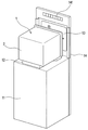
도 2는 상기 로드 포트의 FOUP 지지대에 FOUP가 적재된 상태를 도시하는 사시도.
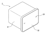
도 3은 상기 로드 포트에 대하여 사용되는 FOUP의 일례를 도시하는 사시도.
도 4는 상기 로드 포트에 있어서의 FOUP 덮개용 센서와 그 광축을 도시하는 주요부 확대 사시도.
11 : 본체부
12 : 지지대
13 : 덮개부
131 : 끼워 맞춤부
14 : 패널부
141 : 표시부
15 : 덮개용 센서
151 : 투광부
152 : 수광부
15L : 광축
2 : FOUP
21 : 본체
22 : 덮개
221 : 피끼워 맞춤부
Claims (4)
- 반도체 웨이퍼의 반송을 위해, 반도체 처리 장치에 있어서의 반출입구에 마련되는 로드 포트에 있어서,
개폐 가능한 FOUP 덮개를 갖고 있으며 내부에 반도체 웨이퍼를 수납할 수 있는 용기인 FOUP를 지지하면서, 상기 반출입구에 대한 전후 방향으로 이동 가능하게 하는 FOUP 지지대와,
상기 반출입구를 개폐하는 덮개부와,
상기 FOUP가 상기 반출입구에 대하여 소정 거리만큼 후퇴한 언로드 완료의 시점에 있어서의, 정상 시의 상기 FOUP 덮개의 위치와 폐쇄 상태인 상기 덮개부의 위치 사이에서 검지하도록 마련된 FOUP 덮개용 센서와,
상기 언로드 완료 이후에 있어서 상기 FOUP 덮개용 센서가 검지하였음을 검출하는 검출부를 구비하는 것을 특징으로 하는 로드 포트. - 제1항에 있어서,
상기 FOUP 덮개용 센서가 광 센서인 것을 특징으로 하는 로드 포트. - 제2항에 있어서,
상기 FOUP 덮개용 센서의 광축이, 전후 방향으로 경사져 있는 로드 포트. - 반도체 웨이퍼의 반송을 위해, 반도체 처리 장치에 있어서의 반출입구에 마련되는 로드 포트이며,
개폐 가능한 FOUP 덮개를 갖고 있으며 내부에 반도체 웨이퍼를 수납할 수 있는 용기인 FOUP를 지지하면서, 상기 반도체 처리 장치의 상기 반출입구에 대한 전후 방향으로 이동 가능하게 하는 FOUP 지지대와,
상기 반출입구를 개폐하는 덮개부와,
상기 FOUP가 상기 반도체 처리 장치의 상기 반출입구에 대하여 소정 거리만큼 후퇴한 언로드 완료의 시점에 있어서의, 정상 시의 상기 FOUP 덮개의 위치와 폐쇄 상태인 상기 덮개부의 위치 사이에서 검지하도록 마련된 FOUP 덮개용 센서를 구비한 로드 포트에 적용되고,
상기 FOUP 덮개를 폐쇄하는 공정과,
상기 FOUP 지지대 상에서 상기 FOUP를 상기 반출입구에 대하여 후퇴시키는 공정과,
상기 FOUP 덮개용 센서에 의해 검지를 행하는 공정
을 상기 기재된 순서대로 행하는 로드 포트의 FOUP 덮개 이상 검지 방법.
Applications Claiming Priority (2)
| Application Number | Priority Date | Filing Date | Title |
|---|---|---|---|
| JPJP-P-2018-191020 | 2018-10-09 | ||
| JP2018191020A JP7228759B2 (ja) | 2018-10-09 | 2018-10-09 | ロードポート及びロードポートのfoup蓋異常検知方法 |
Publications (2)
| Publication Number | Publication Date |
|---|---|
| KR20200040667A true KR20200040667A (ko) | 2020-04-20 |
| KR102778940B1 KR102778940B1 (ko) | 2025-03-11 |
Family
ID=70052392
Family Applications (1)
| Application Number | Title | Priority Date | Filing Date |
|---|---|---|---|
| KR1020190122377A Active KR102778940B1 (ko) | 2018-10-09 | 2019-10-02 | 로드 포트 및 로드 포트의 foup 덮개 이상 검지 방법 |
Country Status (5)
| Country | Link |
|---|---|
| US (1) | US10923377B2 (ko) |
| JP (1) | JP7228759B2 (ko) |
| KR (1) | KR102778940B1 (ko) |
| CN (1) | CN111029285B (ko) |
| TW (1) | TW202014360A (ko) |
Cited By (2)
| Publication number | Priority date | Publication date | Assignee | Title |
|---|---|---|---|---|
| KR20230080656A (ko) * | 2021-11-30 | 2023-06-07 | 세메스 주식회사 | 반도체 이송 장비 |
| KR20230088785A (ko) * | 2020-10-20 | 2023-06-20 | 로제 가부시키가이샤 | 로드 포트 |
Families Citing this family (2)
| Publication number | Priority date | Publication date | Assignee | Title |
|---|---|---|---|---|
| JP2025102459A (ja) * | 2023-12-26 | 2025-07-08 | 東京エレクトロン株式会社 | 検知方法、基板処理システム及び制御プログラム |
| JP7783449B1 (ja) * | 2025-03-26 | 2025-12-09 | 平田機工株式会社 | ロードポート、異常判定方法及び記憶媒体 |
Citations (5)
| Publication number | Priority date | Publication date | Assignee | Title |
|---|---|---|---|---|
| JPH03160744A (ja) * | 1989-11-17 | 1991-07-10 | Hitachi Nakaseiki Ltd | 半導体ウエハ収納装置及びこれを備えたウエハ搬送システム |
| JP2000114350A (ja) * | 1998-09-29 | 2000-04-21 | Sony Corp | ウェーハの検出装置及び検出方法 |
| JP2007123513A (ja) * | 2005-10-27 | 2007-05-17 | Shin Etsu Polymer Co Ltd | 精密基板収納容器 |
| JP2009239004A (ja) * | 2008-03-27 | 2009-10-15 | Tdk Corp | 密閉容器及び該密閉容器の蓋開閉システム、ウエハ搬送システム、及び密閉容器の蓋閉鎖方法 |
| KR20140092249A (ko) * | 2013-01-15 | 2014-07-23 | 도쿄엘렉트론가부시키가이샤 | 기판 수납 처리 장치, 기판 수납 처리 방법, 및 기판 수납 처리용 기억 매체 |
Family Cites Families (17)
| Publication number | Priority date | Publication date | Assignee | Title |
|---|---|---|---|---|
| DE4238834A1 (en) * | 1991-11-18 | 1993-05-19 | Fusion Systems Corp | Robotic semiconductor wafer transporter with vertical photodetector array - scans detectors to determine which slots are occupied by wafers illuminated from emitter on robot arm |
| JP3794861B2 (ja) | 1999-03-16 | 2006-07-12 | Tdk株式会社 | クリーン搬送方法及び装置 |
| JP3954287B2 (ja) | 1999-06-28 | 2007-08-08 | 東京エレクトロン株式会社 | ウェハキャリア用蓋体の着脱装置 |
| JP2002110756A (ja) * | 2000-09-22 | 2002-04-12 | Applied Materials Inc | オープンカセット用ロードポート |
| JP4118592B2 (ja) * | 2002-04-22 | 2008-07-16 | 富士通株式会社 | ロードポート及び半導体製造装置 |
| US6984839B2 (en) * | 2002-11-22 | 2006-01-10 | Tdk Corporation | Wafer processing apparatus capable of mapping wafers |
| KR20040063469A (ko) * | 2003-01-07 | 2004-07-14 | 삼성전자주식회사 | 밀폐형 웨이퍼 카세트 로딩/언로딩 설비 |
| JP4428644B2 (ja) | 2004-06-03 | 2010-03-10 | 平田機工株式会社 | 複数種類の容器に対応可能なfoupオープナの容器認識方法 |
| KR20060007578A (ko) * | 2004-07-20 | 2006-01-26 | 삼성전자주식회사 | 웨이퍼 이송 시스템 |
| KR20070001636A (ko) * | 2005-06-29 | 2007-01-04 | 삼성전자주식회사 | 센서가 장착된 도어와 이를 구비한 웨이퍼 처리 장치 |
| US8821099B2 (en) * | 2005-07-11 | 2014-09-02 | Brooks Automation, Inc. | Load port module |
| JP2010232560A (ja) * | 2009-03-27 | 2010-10-14 | Sinfonia Technology Co Ltd | マッピング機構、foup、及びロードポート |
| JP5518513B2 (ja) * | 2010-02-04 | 2014-06-11 | 平田機工株式会社 | フープオープナ及びその動作方法 |
| JP6455239B2 (ja) * | 2015-03-06 | 2019-01-23 | シンフォニアテクノロジー株式会社 | ドア開閉装置 |
| TW201740495A (zh) * | 2015-11-30 | 2017-11-16 | 昕芙旎雅股份有限公司 | 裝載埠 |
| JP6689672B2 (ja) | 2016-05-25 | 2020-04-28 | 信越ポリマー株式会社 | 基板収納容器及びその管理システム並びに基板収納容器の管理方法 |
| TWI756361B (zh) * | 2017-02-22 | 2022-03-01 | 日商東京威力科創股份有限公司 | 基板收納處理裝置、基板收納處理方法及記錄媒體 |
-
2018
- 2018-10-09 JP JP2018191020A patent/JP7228759B2/ja active Active
-
2019
- 2019-09-30 CN CN201910945294.8A patent/CN111029285B/zh active Active
- 2019-10-02 KR KR1020190122377A patent/KR102778940B1/ko active Active
- 2019-10-02 TW TW108135649A patent/TW202014360A/zh unknown
- 2019-10-03 US US16/592,677 patent/US10923377B2/en active Active
Patent Citations (5)
| Publication number | Priority date | Publication date | Assignee | Title |
|---|---|---|---|---|
| JPH03160744A (ja) * | 1989-11-17 | 1991-07-10 | Hitachi Nakaseiki Ltd | 半導体ウエハ収納装置及びこれを備えたウエハ搬送システム |
| JP2000114350A (ja) * | 1998-09-29 | 2000-04-21 | Sony Corp | ウェーハの検出装置及び検出方法 |
| JP2007123513A (ja) * | 2005-10-27 | 2007-05-17 | Shin Etsu Polymer Co Ltd | 精密基板収納容器 |
| JP2009239004A (ja) * | 2008-03-27 | 2009-10-15 | Tdk Corp | 密閉容器及び該密閉容器の蓋開閉システム、ウエハ搬送システム、及び密閉容器の蓋閉鎖方法 |
| KR20140092249A (ko) * | 2013-01-15 | 2014-07-23 | 도쿄엘렉트론가부시키가이샤 | 기판 수납 처리 장치, 기판 수납 처리 방법, 및 기판 수납 처리용 기억 매체 |
Cited By (2)
| Publication number | Priority date | Publication date | Assignee | Title |
|---|---|---|---|---|
| KR20230088785A (ko) * | 2020-10-20 | 2023-06-20 | 로제 가부시키가이샤 | 로드 포트 |
| KR20230080656A (ko) * | 2021-11-30 | 2023-06-07 | 세메스 주식회사 | 반도체 이송 장비 |
Also Published As
| Publication number | Publication date |
|---|---|
| US10923377B2 (en) | 2021-02-16 |
| JP7228759B2 (ja) | 2023-02-27 |
| KR102778940B1 (ko) | 2025-03-11 |
| TW202014360A (zh) | 2020-04-16 |
| CN111029285A (zh) | 2020-04-17 |
| JP2020061436A (ja) | 2020-04-16 |
| CN111029285B (zh) | 2024-05-14 |
| US20200111695A1 (en) | 2020-04-09 |
Similar Documents
| Publication | Publication Date | Title |
|---|---|---|
| TW434167B (en) | Ergonomic, variable size, bottom opening system compatible with a vertical interface | |
| TWI661496B (zh) | 晶圓映射裝置及具備此裝置之裝載埠 | |
| TWI677933B (zh) | 門開關裝置 | |
| TWI425590B (zh) | 基板處理裝置及其基板搬送方法 | |
| US12068186B2 (en) | Load port module | |
| US20110188977A1 (en) | Foup opener and operating method thereof | |
| KR102778940B1 (ko) | 로드 포트 및 로드 포트의 foup 덮개 이상 검지 방법 | |
| CN111009485B (zh) | 基板仓库、基板处理系统和基板检查方法 | |
| TW201633436A (zh) | 門開閉裝置、搬運裝置、分類裝置、收納容器之開放方法 | |
| US12131933B2 (en) | Load port | |
| JP2009064807A (ja) | 基板位置ずれ検出システム | |
| TWI819160B (zh) | 設備前端模組(efem) | |
| US20100280653A1 (en) | Substrate processing apparatus and semiconductor device manufacturing method | |
| US12249527B2 (en) | Substrate transport apparatus and substrate transport method | |
| CN100407394C (zh) | 基板处理装置及其搬送定位方法 | |
| US20090294442A1 (en) | Lid opening/closing system for closed container, contained object insertion/takeout system having same lid opening/closing system, and substrate processing method using same lid opening/closing system | |
| KR20150027704A (ko) | 로드 포트 장치 및 기판 처리 장치 | |
| JP3730810B2 (ja) | 容器の移動装置および方法 | |
| KR102797917B1 (ko) | 반도체 제조 설비용 웨이퍼의 자동 티칭장치 | |
| KR101425864B1 (ko) | 설치 및 유지 보수가 용이한 센서유닛을 포함하는 핌스 로더 | |
| KR102837595B1 (ko) | 반송 시스템 | |
| JPH11204617A (ja) | 基板検出装置および基板搬入搬出装置 | |
| TW202527213A (zh) | 基板搬送裝置及基板搬送方法 | |
| TW202501687A (zh) | 裝載連接埠 | |
| TW202605999A (zh) | 搬運容器蓋子脫落偵測裝置、載入埠、及搬運容器蓋子脫落偵測方法 |
Legal Events
| Date | Code | Title | Description |
|---|---|---|---|
| PA0109 | Patent application |
St.27 status event code: A-0-1-A10-A12-nap-PA0109 |
|
| PG1501 | Laying open of application |
St.27 status event code: A-1-1-Q10-Q12-nap-PG1501 |
|
| A201 | Request for examination | ||
| PA0201 | Request for examination |
St.27 status event code: A-1-2-D10-D11-exm-PA0201 |
|
| E902 | Notification of reason for refusal | ||
| PE0902 | Notice of grounds for rejection |
St.27 status event code: A-1-2-D10-D21-exm-PE0902 |
|
| P11-X000 | Amendment of application requested |
St.27 status event code: A-2-2-P10-P11-nap-X000 |
|
| P13-X000 | Application amended |
St.27 status event code: A-2-2-P10-P13-nap-X000 |
|
| E701 | Decision to grant or registration of patent right | ||
| PE0701 | Decision of registration |
St.27 status event code: A-1-2-D10-D22-exm-PE0701 |
|
| GRNT | Written decision to grant | ||
| PR0701 | Registration of establishment |
St.27 status event code: A-2-4-F10-F11-exm-PR0701 |
|
| PR1002 | Payment of registration fee |
St.27 status event code: A-2-2-U10-U11-oth-PR1002 Fee payment year number: 1 |
|
| PG1601 | Publication of registration |
St.27 status event code: A-4-4-Q10-Q13-nap-PG1601 |
|
| P22-X000 | Classification modified |
St.27 status event code: A-4-4-P10-P22-nap-X000 |