KR20200040873A - Nand 온도 데이터 관리 - Google Patents
Nand 온도 데이터 관리 Download PDFInfo
- Publication number
- KR20200040873A KR20200040873A KR1020207008679A KR20207008679A KR20200040873A KR 20200040873 A KR20200040873 A KR 20200040873A KR 1020207008679 A KR1020207008679 A KR 1020207008679A KR 20207008679 A KR20207008679 A KR 20207008679A KR 20200040873 A KR20200040873 A KR 20200040873A
- Authority
- KR
- South Korea
- Prior art keywords
- temperature
- nand
- data
- representation
- memory
- Prior art date
- Legal status (The legal status is an assumption and is not a legal conclusion. Google has not performed a legal analysis and makes no representation as to the accuracy of the status listed.)
- Ceased
Links
Images




Classifications
-
- G—PHYSICS
- G11—INFORMATION STORAGE
- G11C—STATIC STORES
- G11C16/00—Erasable programmable read-only memories
- G11C16/02—Erasable programmable read-only memories electrically programmable
- G11C16/06—Auxiliary circuits, e.g. for writing into memory
- G11C16/10—Programming or data input circuits
-
- G—PHYSICS
- G11—INFORMATION STORAGE
- G11C—STATIC STORES
- G11C16/00—Erasable programmable read-only memories
- G11C16/02—Erasable programmable read-only memories electrically programmable
- G11C16/06—Auxiliary circuits, e.g. for writing into memory
- G11C16/34—Determination of programming status, e.g. threshold voltage, overprogramming or underprogramming, retention
- G11C16/3418—Disturbance prevention or evaluation; Refreshing of disturbed memory data
- G11C16/3427—Circuits or methods to prevent or reduce disturbance of the state of a memory cell when neighbouring cells are read or written
-
- G—PHYSICS
- G06—COMPUTING OR CALCULATING; COUNTING
- G06F—ELECTRIC DIGITAL DATA PROCESSING
- G06F12/00—Accessing, addressing or allocating within memory systems or architectures
- G06F12/02—Addressing or allocation; Relocation
- G06F12/0223—User address space allocation, e.g. contiguous or non contiguous base addressing
- G06F12/023—Free address space management
- G06F12/0238—Memory management in non-volatile memory, e.g. resistive RAM or ferroelectric memory
- G06F12/0246—Memory management in non-volatile memory, e.g. resistive RAM or ferroelectric memory in block erasable memory, e.g. flash memory
-
- G—PHYSICS
- G11—INFORMATION STORAGE
- G11C—STATIC STORES
- G11C11/00—Digital stores characterised by the use of particular electric or magnetic storage elements; Storage elements therefor
- G11C11/56—Digital stores characterised by the use of particular electric or magnetic storage elements; Storage elements therefor using storage elements with more than two stable states represented by steps, e.g. of voltage, current, phase, frequency
- G11C11/5621—Digital stores characterised by the use of particular electric or magnetic storage elements; Storage elements therefor using storage elements with more than two stable states represented by steps, e.g. of voltage, current, phase, frequency using charge storage in a floating gate
- G11C11/5628—Programming or writing circuits; Data input circuits
-
- G—PHYSICS
- G11—INFORMATION STORAGE
- G11C—STATIC STORES
- G11C11/00—Digital stores characterised by the use of particular electric or magnetic storage elements; Storage elements therefor
- G11C11/56—Digital stores characterised by the use of particular electric or magnetic storage elements; Storage elements therefor using storage elements with more than two stable states represented by steps, e.g. of voltage, current, phase, frequency
- G11C11/5621—Digital stores characterised by the use of particular electric or magnetic storage elements; Storage elements therefor using storage elements with more than two stable states represented by steps, e.g. of voltage, current, phase, frequency using charge storage in a floating gate
- G11C11/5642—Sensing or reading circuits; Data output circuits
-
- G—PHYSICS
- G11—INFORMATION STORAGE
- G11C—STATIC STORES
- G11C16/00—Erasable programmable read-only memories
- G11C16/02—Erasable programmable read-only memories electrically programmable
- G11C16/04—Erasable programmable read-only memories electrically programmable using variable threshold transistors, e.g. FAMOS
- G11C16/0483—Erasable programmable read-only memories electrically programmable using variable threshold transistors, e.g. FAMOS comprising cells having several storage transistors connected in series
-
- G—PHYSICS
- G11—INFORMATION STORAGE
- G11C—STATIC STORES
- G11C16/00—Erasable programmable read-only memories
- G11C16/02—Erasable programmable read-only memories electrically programmable
- G11C16/06—Auxiliary circuits, e.g. for writing into memory
- G11C16/10—Programming or data input circuits
- G11C16/20—Initialising; Data preset; Chip identification
-
- G—PHYSICS
- G11—INFORMATION STORAGE
- G11C—STATIC STORES
- G11C16/00—Erasable programmable read-only memories
- G11C16/02—Erasable programmable read-only memories electrically programmable
- G11C16/06—Auxiliary circuits, e.g. for writing into memory
- G11C16/22—Safety or protection circuits preventing unauthorised or accidental access to memory cells
-
- G—PHYSICS
- G11—INFORMATION STORAGE
- G11C—STATIC STORES
- G11C16/00—Erasable programmable read-only memories
- G11C16/02—Erasable programmable read-only memories electrically programmable
- G11C16/06—Auxiliary circuits, e.g. for writing into memory
- G11C16/26—Sensing or reading circuits; Data output circuits
- G11C16/28—Sensing or reading circuits; Data output circuits using differential sensing or reference cells, e.g. dummy cells
-
- G—PHYSICS
- G11—INFORMATION STORAGE
- G11C—STATIC STORES
- G11C16/00—Erasable programmable read-only memories
- G11C16/02—Erasable programmable read-only memories electrically programmable
- G11C16/06—Auxiliary circuits, e.g. for writing into memory
- G11C16/34—Determination of programming status, e.g. threshold voltage, overprogramming or underprogramming, retention
- G11C16/3418—Disturbance prevention or evaluation; Refreshing of disturbed memory data
-
- G—PHYSICS
- G11—INFORMATION STORAGE
- G11C—STATIC STORES
- G11C29/00—Checking stores for correct operation ; Subsequent repair; Testing stores during standby or offline operation
- G11C29/02—Detection or location of defective auxiliary circuits, e.g. defective refresh counters
- G11C29/021—Detection or location of defective auxiliary circuits, e.g. defective refresh counters in voltage or current generators
-
- G—PHYSICS
- G11—INFORMATION STORAGE
- G11C—STATIC STORES
- G11C29/00—Checking stores for correct operation ; Subsequent repair; Testing stores during standby or offline operation
- G11C29/02—Detection or location of defective auxiliary circuits, e.g. defective refresh counters
- G11C29/028—Detection or location of defective auxiliary circuits, e.g. defective refresh counters with adaption or trimming of parameters
-
- G—PHYSICS
- G11—INFORMATION STORAGE
- G11C—STATIC STORES
- G11C7/00—Arrangements for writing information into, or reading information out from, a digital store
- G11C7/04—Arrangements for writing information into, or reading information out from, a digital store with means for avoiding disturbances due to temperature effects
-
- G—PHYSICS
- G06—COMPUTING OR CALCULATING; COUNTING
- G06F—ELECTRIC DIGITAL DATA PROCESSING
- G06F2212/00—Indexing scheme relating to accessing, addressing or allocation within memory systems or architectures
- G06F2212/72—Details relating to flash memory management
- G06F2212/7202—Allocation control and policies
-
- G—PHYSICS
- G06—COMPUTING OR CALCULATING; COUNTING
- G06F—ELECTRIC DIGITAL DATA PROCESSING
- G06F2212/00—Indexing scheme relating to accessing, addressing or allocation within memory systems or architectures
- G06F2212/72—Details relating to flash memory management
- G06F2212/7207—Details relating to flash memory management management of metadata or control data
-
- G—PHYSICS
- G11—INFORMATION STORAGE
- G11C—STATIC STORES
- G11C2211/00—Indexing scheme relating to digital stores characterized by the use of particular electric or magnetic storage elements; Storage elements therefor
- G11C2211/56—Indexing scheme relating to G11C11/56 and sub-groups for features not covered by these groups
- G11C2211/564—Miscellaneous aspects
- G11C2211/5641—Multilevel memory having cells with different number of storage levels
Landscapes
- Engineering & Computer Science (AREA)
- Computer Hardware Design (AREA)
- Microelectronics & Electronic Packaging (AREA)
- Computer Security & Cryptography (AREA)
- Theoretical Computer Science (AREA)
- Physics & Mathematics (AREA)
- General Engineering & Computer Science (AREA)
- General Physics & Mathematics (AREA)
- Read Only Memory (AREA)
Abstract
Description
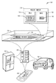
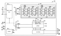
도 1은 메모리 디바이스를 포함하는 환경의 예를 도시하는 도면.
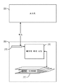
도 2는 NAND 온도 데이터 관리를 위한 시스템의 예시적인 블록도.
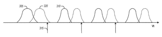
도 3은 상이한 온도 기입 조건 동안 셀 전압 드리프트의 예를 도시하는 도면.
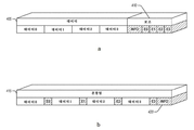
도 4a 및 도 4b는 NAND 온도 데이터를 위한 저장 구성을 도시하는 도면.
도 5 및 도 6은 3D NAND 아키텍처 반도체 메모리 어레이의 예의 개략도.
도 7은 메모리 모듈의 예시적인 블록도.
도 8은 NAND 온도 데이터 관리를 위한 방법의 흐름도.
도 9는 하나 이상의 실시형태가 구현될 수도 있는 기계의 예를 도시하는 블록도.
Claims (30)
- NAND 온도 데이터 관리를 위한 NAND 디바이스로서,
NAND 구성 요소; 및
NAND 제어기를 포함하되, NAND 제어기는,
명령어를 수신하여 데이터를 상기 NAND 구성 요소에 기입하고;
상기 명령어를 수신하는 것에 응답하여 상기 NAND 구성 요소에 대응하는 온도를 획득하고; 그리고
상기 명령어를 실행하여 데이터를 상기 NAND 구성 요소에 기입하고 그리고 온도의 표현을 기입하기 위한 것이고, 상기 데이터는 사용자 부분에 기입되고 그리고 상기 온도의 표현은 상기 NAND 제어기에만 액세스 가능하고 그리고 상기 사용자 부분으로부터 분리되는 관리 부분에 기입되는, NAND 디바이스. - 제1항에 있어서, 상기 관리 부분은 상기 NAND 구성 요소에 있는, NAND 디바이스.
- 제2항에 있어서, 상기 NAND 구성 요소는 페이지인, NAND 디바이스.
- 제3항에 있어서, 상기 관리 부분은 상기 페이지의 보조 바이트인, NAND 디바이스.
- 제1항에 있어서, 상기 온도의 표현은 획득된 온도보다 더 낮은 레졸루션(resolution)에서 상기 온도의 양자화인, NAND 디바이스.
- 제1항에 있어서, 상기 온도를 획득하기 위해서, 상기 NAND 제어기는 상기 명령어를 수신하는 것에 응답하여 온도계로부터 상기 온도를 획득하는, NAND 디바이스.
- 제1항에 있어서, 상기 NAND 제어기는 상기 NAND 구성 요소로부터 상기 데이터를 더 판독하고 그리고 상기 온도의 표현을 판독하는, NAND 디바이스.
- 제7항에 있어서, 상기 NAND 제어기는 판독 명령어를 수신하는 것에 응답하여 상기 데이터를 판독하고, 그리고 상기 온도의 표현은 상기 데이터에 대한 판독 전압을 정정하여 판독 오류를 감소시키도록 사용되는, NAND 디바이스.
- 제8항에 있어서, 상기 온도의 표현은 상기 판독 명령어를 호출하는 호스트에 제공되고, 그리고 상기 호스트는 상기 온도의 표현을 사용하여 상기 판독 전압을 정정하는, NAND 디바이스.
- 제7항에 있어서, 상기 NAND 제어기는 상기 NAND 디바이스의 전력 켜짐 상태에 응답하여 상기 데이터를 판독하고, 그리고 상기 온도의 표현은 미래의 판독 작동(operation)을 위해 휘발성 메모리에 저장되는, NAND 디바이스.
- NAND 온도 데이터 관리를 위한 방법으로서,
NAND 디바이스의 제어기에서, 명령어를 수신하여 데이터를 상기 NAND 디바이스 내 NAND 구성 요소에 기입하는 단계;
상기 명령어를 수신하는 것에 응답하여 상기 NAND 구성 요소에 대응하는 온도를 획득하는 단계; 및
상기 명령어를 실행하여 데이터를 상기 NAND 구성 요소에 기입하고 그리고 온도의 표현을 기입하는 단계를 포함하되, 상기 데이터는 사용자 부분에 기입되고 그리고 상기 온도의 표현은 상기 제어기에만 액세스 가능하고 그리고 상기 사용자 부분으로부터 분리되는 관리 부분에 기입되는, NAND 온도 데이터 관리를 위한 방법. - 제11항에 있어서, 상기 관리 부분은 상기 NAND 구성 요소에 있는, NAND 온도 데이터 관리를 위한 방법.
- 제12항에 있어서, 상기 NAND 구성 요소는 페이지인, NAND 온도 데이터 관리를 위한 방법.
- 제13항에 있어서, 상기 관리 부분은 상기 페이지의 보조 바이트인, NAND 온도 데이터 관리를 위한 방법.
- 제11항에 있어서, 상기 온도의 표현은 획득된 온도보다 더 낮은 레졸루션에서 상기 온도의 양자화인, NAND 온도 데이터 관리를 위한 방법.
- 제11항에 있어서, 상기 온도를 획득하는 것은 상기 명령어를 수신하는 것에 응답하여 온도계로부터 상기 온도를 획득하는 것을 포함하는, NAND 온도 데이터 관리를 위한 방법.
- 제11항에 있어서, 상기 NAND 구성 요소로부터 상기 데이터를 판독하고 그리고 상기 온도의 표현을 판독하는 단계를 포함하는, NAND 온도 데이터 관리를 위한 방법.
- 제17항에 있어서, 상기 데이터를 판독하는 것은 상기 제어기에서 판독 명령어를 수신하는 것에 응답하고, 그리고 상기 온도의 표현은 상기 데이터에 대한 판독 전압을 정정하여 판독 오류를 감소시키도록 사용되는, NAND 온도 데이터 관리를 위한 방법.
- 제18항에 있어서, 상기 온도의 표현은 상기 판독 명령어를 호출하는 호스트에 제공되고, 그리고 상기 호스트는 상기 온도의 표현을 사용하여 상기 판독 전압을 정정하는, NAND 온도 데이터 관리를 위한 방법.
- 제17항에 있어서, 상기 데이터를 판독하는 것은 상기 NAND 디바이스의 전력 켜짐 상태에 응답하고, 그리고 상기 온도의 표현은 미래의 판독 작동을 위해 휘발성 메모리에 저장되는, NAND 온도 데이터 관리를 위한 방법.
- 처리 회로망에 의해 실행될 때, 상기 처리 회로망이 작동을 수행하게 하는 명령을 포함하는 적어도 하나의 기계 판독 가능 매체로서, 상기 작동은,
NAND 디바이스의 제어기에서, 명령어를 수신하여 데이터를 상기 NAND 디바이스 내 NAND 구성 요소에 기입하는 것;
상기 명령어를 수신하는 것에 응답하여 상기 NAND 구성 요소에 대응하는 온도를 획득하는 것; 및
상기 명령어를 실행하여 데이터를 상기 NAND 구성 요소에 기입하고 그리고 온도의 표현을 기입하는 것을 포함하되, 상기 데이터는 사용자 부분에 기입되고 그리고 상기 온도의 표현은 상기 제어기에만 액세스 가능하고 그리고 상기 사용자 부분으로부터 분리되는 관리 부분에 기입되는, 기계 판독 가능 매체. - 제21항에 있어서, 상기 관리 부분은 상기 NAND 구성 요소에 있는, 기계 판독 가능 매체.
- 제22항에 있어서, 상기 NAND 구성 요소는 페이지인, 기계 판독 가능 매체.
- 제23항에 있어서, 상기 관리 부분은 상기 페이지의 보조 바이트인, 기계 판독 가능 매체.
- 제21항에 있어서, 상기 온도의 표현은 획득된 온도보다 더 낮은 레졸루션에서 상기 온도의 양자화인, 기계 판독 가능 매체.
- 제21항에 있어서, 상기 온도를 획득하는 것은 상기 명령어를 수신하는 것에 응답하여 온도계로부터 상기 온도를 획득하는 것을 포함하는, 기계 판독 가능 매체.
- 제21항에 있어서, 상기 작동은 상기 NAND 구성 요소로부터 상기 데이터를 판독하는 것 및 상기 온도의 표현을 판독하는 것을 포함하는, 기계 판독 가능 매체.
- 제27항에 있어서, 상기 데이터를 판독하는 것은 상기 제어기에서 판독 명령어를 수신하는 것에 응답하고, 그리고 상기 온도의 표현은 상기 데이터에 대한 판독 전압을 정정하여 판독 오류를 감소시키도록 사용되는, 기계 판독 가능 매체.
- 제28항에 있어서, 상기 온도의 표현은 상기 판독 명령어를 호출하는 호스트에 제공되고, 그리고 상기 호스트는 상기 온도의 표현을 사용하여 상기 판독 전압을 정정하는, 기계 판독 가능 매체.
- 제27항에 있어서, 상기 데이터를 판독하는 것은 상기 NAND 디바이스의 전력 켜짐 상태에 응답하고, 그리고 상기 온도의 표현은 미래의 판독 작동을 위해 휘발성 메모리에 저장되는, 기계 판독 가능 매체.
Priority Applications (1)
| Application Number | Priority Date | Filing Date | Title |
|---|---|---|---|
| KR1020227015563A KR20220066189A (ko) | 2017-08-30 | 2018-08-29 | Nand 온도 데이터 관리 |
Applications Claiming Priority (3)
| Application Number | Priority Date | Filing Date | Title |
|---|---|---|---|
| US15/690,920 | 2017-08-30 | ||
| US15/690,920 US10354732B2 (en) | 2017-08-30 | 2017-08-30 | NAND temperature data management |
| PCT/US2018/048452 WO2019046370A1 (en) | 2017-08-30 | 2018-08-29 | MANAGEMENT OF NAND TEMPERATURE DATA |
Related Child Applications (1)
| Application Number | Title | Priority Date | Filing Date |
|---|---|---|---|
| KR1020227015563A Division KR20220066189A (ko) | 2017-08-30 | 2018-08-29 | Nand 온도 데이터 관리 |
Publications (1)
| Publication Number | Publication Date |
|---|---|
| KR20200040873A true KR20200040873A (ko) | 2020-04-20 |
Family
ID=65437633
Family Applications (2)
| Application Number | Title | Priority Date | Filing Date |
|---|---|---|---|
| KR1020227015563A Ceased KR20220066189A (ko) | 2017-08-30 | 2018-08-29 | Nand 온도 데이터 관리 |
| KR1020207008679A Ceased KR20200040873A (ko) | 2017-08-30 | 2018-08-29 | Nand 온도 데이터 관리 |
Family Applications Before (1)
| Application Number | Title | Priority Date | Filing Date |
|---|---|---|---|
| KR1020227015563A Ceased KR20220066189A (ko) | 2017-08-30 | 2018-08-29 | Nand 온도 데이터 관리 |
Country Status (5)
| Country | Link |
|---|---|
| US (4) | US10354732B2 (ko) |
| EP (1) | EP3676843B1 (ko) |
| KR (2) | KR20220066189A (ko) |
| CN (1) | CN111183483B (ko) |
| WO (1) | WO2019046370A1 (ko) |
Families Citing this family (12)
| Publication number | Priority date | Publication date | Assignee | Title |
|---|---|---|---|---|
| US10553301B2 (en) * | 2017-06-03 | 2020-02-04 | Sandisk Technologies Llc | Dynamic read table block filter |
| US10354732B2 (en) | 2017-08-30 | 2019-07-16 | Micron Technology, Inc. | NAND temperature data management |
| CN111951867B (zh) * | 2019-05-14 | 2022-11-01 | 兆易创新科技集团股份有限公司 | 一种控制读操作的方法和装置 |
| US20210056391A1 (en) * | 2019-08-20 | 2021-02-25 | Mind Machine Learning, Inc. | Systems and Methods for Simulating Sense Data and Creating Perceptions |
| US11062756B2 (en) | 2019-10-14 | 2021-07-13 | Western Digital Technologies, Inc. | Extending operating temperature of storage device |
| KR102830262B1 (ko) | 2020-11-17 | 2025-07-03 | 삼성전자주식회사 | 스토리지 장치, 스토리지 장치를 포함하는 서버 장치 및 스토리지 장치의 구동 방법 |
| US20220229580A1 (en) * | 2021-01-20 | 2022-07-21 | Micron Technology, Inc. | Temperature tracking for a memory system |
| US11520661B1 (en) | 2021-07-12 | 2022-12-06 | Apple Inc. | Scheduling of data refresh in a memory based on decoding latencies |
| US12067290B2 (en) * | 2021-08-31 | 2024-08-20 | Micron Technology, Inc. | On-die cross-temperature management for a memory device |
| CN115410640B (zh) * | 2022-09-15 | 2026-03-27 | 长鑫存储技术有限公司 | 测试方法、装置、设备及存储介质 |
| JP7848092B2 (ja) * | 2022-09-20 | 2026-04-20 | キオクシア株式会社 | メモリシステム |
| CN118445216B (zh) * | 2023-11-28 | 2025-03-25 | 荣耀终端股份有限公司 | 一种数据读写方法、电子设备、存储介质及芯片 |
Family Cites Families (19)
| Publication number | Priority date | Publication date | Assignee | Title |
|---|---|---|---|---|
| US7366819B2 (en) * | 2004-02-11 | 2008-04-29 | Infineon Technologies Ag | Fast unaligned cache access system and method |
| US7639542B2 (en) * | 2006-05-15 | 2009-12-29 | Apple Inc. | Maintenance operations for multi-level data storage cells |
| US8248856B2 (en) | 2010-10-20 | 2012-08-21 | Seagate Technology Llc | Predictive read channel configuration |
| US8737138B2 (en) * | 2010-11-18 | 2014-05-27 | Micron Technology, Inc. | Memory instruction including parameter to affect operating condition of memory |
| US8472274B2 (en) * | 2011-03-02 | 2013-06-25 | Apple Inc. | Using temperature sensors with a memory device |
| JP5624510B2 (ja) * | 2011-04-08 | 2014-11-12 | 株式会社東芝 | 記憶装置、記憶システム及び認証方法 |
| KR20120125791A (ko) | 2011-05-09 | 2012-11-19 | 삼성전자주식회사 | 플래시 메모리 장치 및 이를 포함하는 메모리 시스템 |
| JP5740296B2 (ja) | 2011-12-16 | 2015-06-24 | 株式会社東芝 | 半導体記憶装置、半導体記憶装置の制御方法、制御プログラム |
| JP6443794B2 (ja) * | 2013-08-16 | 2018-12-26 | エルエスアイ コーポレーション | ホストとコントローラとの間でパーティション化された変換レイヤ |
| KR102211126B1 (ko) | 2014-04-17 | 2021-02-02 | 삼성전자주식회사 | 동작 성능을 조절하는 메모리 시스템 및 메모리 시스템의 동작방법 |
| KR20150121562A (ko) | 2014-04-21 | 2015-10-29 | 삼성전자주식회사 | 비휘발성 메모리 시스템 및 비휘발성 메모리 시스템의 동작방법 |
| KR102248276B1 (ko) * | 2014-05-26 | 2021-05-07 | 삼성전자주식회사 | 스토리지 장치의 동작 방법 |
| US10078546B2 (en) * | 2014-10-24 | 2018-09-18 | Micron Technology, Inc. | Temperature related error management |
| KR20160073868A (ko) | 2014-12-17 | 2016-06-27 | 에스케이하이닉스 주식회사 | 메모리 시스템 및 메모리 시스템의 동작 방법 |
| US10446242B2 (en) * | 2016-05-27 | 2019-10-15 | Western Digital Technologies, Inc. | Temperature variation compensation |
| US9996281B2 (en) * | 2016-03-04 | 2018-06-12 | Western Digital Technologies, Inc. | Temperature variation compensation |
| KR102512448B1 (ko) | 2016-03-28 | 2023-03-22 | 에스케이하이닉스 주식회사 | 메모리 시스템 및 그의 동작 방법 |
| US10115458B2 (en) * | 2016-03-30 | 2018-10-30 | Toshiba Memory Corporation | Perform read or write on a non-volatile memory having a pending read or write based on temperature thereof |
| US10354732B2 (en) | 2017-08-30 | 2019-07-16 | Micron Technology, Inc. | NAND temperature data management |
-
2017
- 2017-08-30 US US15/690,920 patent/US10354732B2/en active Active
-
2018
- 2018-08-29 KR KR1020227015563A patent/KR20220066189A/ko not_active Ceased
- 2018-08-29 WO PCT/US2018/048452 patent/WO2019046370A1/en not_active Ceased
- 2018-08-29 CN CN201880064074.8A patent/CN111183483B/zh active Active
- 2018-08-29 KR KR1020207008679A patent/KR20200040873A/ko not_active Ceased
- 2018-08-29 EP EP18852432.6A patent/EP3676843B1/en active Active
-
2019
- 2019-07-05 US US16/504,039 patent/US10679704B2/en active Active
-
2020
- 2020-04-23 US US16/856,955 patent/US11037630B2/en active Active
-
2021
- 2021-05-26 US US17/331,395 patent/US11610632B2/en active Active
Also Published As
| Publication number | Publication date |
|---|---|
| EP3676843A1 (en) | 2020-07-08 |
| US20200258578A1 (en) | 2020-08-13 |
| WO2019046370A1 (en) | 2019-03-07 |
| US20190333585A1 (en) | 2019-10-31 |
| US11037630B2 (en) | 2021-06-15 |
| US20190066792A1 (en) | 2019-02-28 |
| CN111183483B (zh) | 2023-09-29 |
| US11610632B2 (en) | 2023-03-21 |
| KR20220066189A (ko) | 2022-05-23 |
| EP3676843B1 (en) | 2024-10-02 |
| US10354732B2 (en) | 2019-07-16 |
| CN111183483A (zh) | 2020-05-19 |
| US10679704B2 (en) | 2020-06-09 |
| US20210287748A1 (en) | 2021-09-16 |
| EP3676843A4 (en) | 2021-06-23 |
Similar Documents
| Publication | Publication Date | Title |
|---|---|---|
| US10529434B2 (en) | Detecting power loss in NAND memory devices | |
| US11610632B2 (en) | NAND temperature data management | |
| US11688473B2 (en) | SLC page read | |
| CN112424865B (zh) | Nand温度感知操作 | |
| US10522229B2 (en) | Secure erase for data corruption | |
| US11456037B2 (en) | Block read count voltage adjustment | |
| US10891072B2 (en) | NAND flash thermal alerting | |
| KR20210014209A (ko) | 온도 감응 nand 프로그래밍 | |
| US10325670B2 (en) | Erase page check | |
| KR20200036050A (ko) | 리플로우-보호 | |
| US20190065108A1 (en) | Correcting power loss in nand memory devices | |
| US20210264988A1 (en) | Charge loss compensation | |
| US10437734B2 (en) | Memory constrained translation table management | |
| US20240354005A1 (en) | Managed non-volatile memory device with data verification |
Legal Events
| Date | Code | Title | Description |
|---|---|---|---|
| PA0105 | International application |
Patent event date: 20200325 Patent event code: PA01051R01D Comment text: International Patent Application |
|
| A201 | Request for examination | ||
| PA0201 | Request for examination |
Patent event code: PA02012R01D Patent event date: 20200408 Comment text: Request for Examination of Application |
|
| PG1501 | Laying open of application | ||
| E902 | Notification of reason for refusal | ||
| PE0902 | Notice of grounds for rejection |
Comment text: Notification of reason for refusal Patent event date: 20210223 Patent event code: PE09021S01D |
|
| AMND | Amendment | ||
| E902 | Notification of reason for refusal | ||
| PE0902 | Notice of grounds for rejection |
Comment text: Notification of reason for refusal Patent event date: 20210810 Patent event code: PE09021S01D |
|
| AMND | Amendment | ||
| E601 | Decision to refuse application | ||
| PE0601 | Decision on rejection of patent |
Patent event date: 20220214 Comment text: Decision to Refuse Application Patent event code: PE06012S01D Patent event date: 20210810 Comment text: Notification of reason for refusal Patent event code: PE06011S01I Patent event date: 20210223 Comment text: Notification of reason for refusal Patent event code: PE06011S01I |
|
| X091 | Application refused [patent] | ||
| AMND | Amendment | ||
| PX0901 | Re-examination |
Patent event code: PX09011S01I Patent event date: 20220214 Comment text: Decision to Refuse Application Patent event code: PX09012R01I Patent event date: 20211012 Comment text: Amendment to Specification, etc. Patent event code: PX09012R01I Patent event date: 20210421 Comment text: Amendment to Specification, etc. |
|
| PX0601 | Decision of rejection after re-examination |
Comment text: Decision to Refuse Application Patent event code: PX06014S01D Patent event date: 20220407 Comment text: Amendment to Specification, etc. Patent event code: PX06012R01I Patent event date: 20220316 Comment text: Decision to Refuse Application Patent event code: PX06011S01I Patent event date: 20220214 Comment text: Amendment to Specification, etc. Patent event code: PX06012R01I Patent event date: 20211012 Comment text: Notification of reason for refusal Patent event code: PX06013S01I Patent event date: 20210810 Comment text: Amendment to Specification, etc. Patent event code: PX06012R01I Patent event date: 20210421 Comment text: Notification of reason for refusal Patent event code: PX06013S01I Patent event date: 20210223 |
|
| X601 | Decision of rejection after re-examination | ||
| A107 | Divisional application of patent | ||
| PA0104 | Divisional application for international application |
Comment text: Divisional Application for International Patent Patent event code: PA01041R01D Patent event date: 20220509 |