KR20200040980A - 표시 장치 - Google Patents
표시 장치 Download PDFInfo
- Publication number
- KR20200040980A KR20200040980A KR1020180120723A KR20180120723A KR20200040980A KR 20200040980 A KR20200040980 A KR 20200040980A KR 1020180120723 A KR1020180120723 A KR 1020180120723A KR 20180120723 A KR20180120723 A KR 20180120723A KR 20200040980 A KR20200040980 A KR 20200040980A
- Authority
- KR
- South Korea
- Prior art keywords
- layer
- light
- substrate
- color filter
- disposed
- Prior art date
- Legal status (The legal status is an assumption and is not a legal conclusion. Google has not performed a legal analysis and makes no representation as to the accuracy of the status listed.)
- Granted
Links
Images










Classifications
-
- G—PHYSICS
- G02—OPTICS
- G02F—OPTICAL DEVICES OR ARRANGEMENTS FOR THE CONTROL OF LIGHT BY MODIFICATION OF THE OPTICAL PROPERTIES OF THE MEDIA OF THE ELEMENTS INVOLVED THEREIN; NON-LINEAR OPTICS; FREQUENCY-CHANGING OF LIGHT; OPTICAL LOGIC ELEMENTS; OPTICAL ANALOGUE/DIGITAL CONVERTERS
- G02F1/00—Devices or arrangements for the control of the intensity, colour, phase, polarisation or direction of light arriving from an independent light source, e.g. switching, gating or modulating; Non-linear optics
- G02F1/01—Devices or arrangements for the control of the intensity, colour, phase, polarisation or direction of light arriving from an independent light source, e.g. switching, gating or modulating; Non-linear optics for the control of the intensity, phase, polarisation or colour
- G02F1/13—Devices or arrangements for the control of the intensity, colour, phase, polarisation or direction of light arriving from an independent light source, e.g. switching, gating or modulating; Non-linear optics for the control of the intensity, phase, polarisation or colour based on liquid crystals, e.g. single liquid crystal display cells
- G02F1/133—Constructional arrangements; Operation of liquid crystal cells; Circuit arrangements
- G02F1/1333—Constructional arrangements; Manufacturing methods
- G02F1/1335—Structural association of cells with optical devices, e.g. polarisers or reflectors
- G02F1/133509—Filters, e.g. light shielding masks
- G02F1/133514—Colour filters
-
- G—PHYSICS
- G02—OPTICS
- G02B—OPTICAL ELEMENTS, SYSTEMS OR APPARATUS
- G02B5/00—Optical elements other than lenses
- G02B5/30—Polarising elements
- G02B5/3025—Polarisers, i.e. arrangements capable of producing a definite output polarisation state from an unpolarised input state
- G02B5/3058—Polarisers, i.e. arrangements capable of producing a definite output polarisation state from an unpolarised input state comprising electrically conductive elements, e.g. wire grids, conductive particles
-
- G—PHYSICS
- G02—OPTICS
- G02F—OPTICAL DEVICES OR ARRANGEMENTS FOR THE CONTROL OF LIGHT BY MODIFICATION OF THE OPTICAL PROPERTIES OF THE MEDIA OF THE ELEMENTS INVOLVED THEREIN; NON-LINEAR OPTICS; FREQUENCY-CHANGING OF LIGHT; OPTICAL LOGIC ELEMENTS; OPTICAL ANALOGUE/DIGITAL CONVERTERS
- G02F1/00—Devices or arrangements for the control of the intensity, colour, phase, polarisation or direction of light arriving from an independent light source, e.g. switching, gating or modulating; Non-linear optics
- G02F1/01—Devices or arrangements for the control of the intensity, colour, phase, polarisation or direction of light arriving from an independent light source, e.g. switching, gating or modulating; Non-linear optics for the control of the intensity, phase, polarisation or colour
- G02F1/13—Devices or arrangements for the control of the intensity, colour, phase, polarisation or direction of light arriving from an independent light source, e.g. switching, gating or modulating; Non-linear optics for the control of the intensity, phase, polarisation or colour based on liquid crystals, e.g. single liquid crystal display cells
- G02F1/133—Constructional arrangements; Operation of liquid crystal cells; Circuit arrangements
- G02F1/1333—Constructional arrangements; Manufacturing methods
- G02F1/1335—Structural association of cells with optical devices, e.g. polarisers or reflectors
- G02F1/133509—Filters, e.g. light shielding masks
-
- G—PHYSICS
- G02—OPTICS
- G02B—OPTICAL ELEMENTS, SYSTEMS OR APPARATUS
- G02B5/00—Optical elements other than lenses
- G02B5/30—Polarising elements
- G02B5/3025—Polarisers, i.e. arrangements capable of producing a definite output polarisation state from an unpolarised input state
-
- G—PHYSICS
- G02—OPTICS
- G02F—OPTICAL DEVICES OR ARRANGEMENTS FOR THE CONTROL OF LIGHT BY MODIFICATION OF THE OPTICAL PROPERTIES OF THE MEDIA OF THE ELEMENTS INVOLVED THEREIN; NON-LINEAR OPTICS; FREQUENCY-CHANGING OF LIGHT; OPTICAL LOGIC ELEMENTS; OPTICAL ANALOGUE/DIGITAL CONVERTERS
- G02F1/00—Devices or arrangements for the control of the intensity, colour, phase, polarisation or direction of light arriving from an independent light source, e.g. switching, gating or modulating; Non-linear optics
- G02F1/01—Devices or arrangements for the control of the intensity, colour, phase, polarisation or direction of light arriving from an independent light source, e.g. switching, gating or modulating; Non-linear optics for the control of the intensity, phase, polarisation or colour
- G02F1/13—Devices or arrangements for the control of the intensity, colour, phase, polarisation or direction of light arriving from an independent light source, e.g. switching, gating or modulating; Non-linear optics for the control of the intensity, phase, polarisation or colour based on liquid crystals, e.g. single liquid crystal display cells
- G02F1/133—Constructional arrangements; Operation of liquid crystal cells; Circuit arrangements
- G02F1/1333—Constructional arrangements; Manufacturing methods
- G02F1/1335—Structural association of cells with optical devices, e.g. polarisers or reflectors
- G02F1/133504—Diffusing, scattering, diffracting elements
-
- G—PHYSICS
- G02—OPTICS
- G02F—OPTICAL DEVICES OR ARRANGEMENTS FOR THE CONTROL OF LIGHT BY MODIFICATION OF THE OPTICAL PROPERTIES OF THE MEDIA OF THE ELEMENTS INVOLVED THEREIN; NON-LINEAR OPTICS; FREQUENCY-CHANGING OF LIGHT; OPTICAL LOGIC ELEMENTS; OPTICAL ANALOGUE/DIGITAL CONVERTERS
- G02F1/00—Devices or arrangements for the control of the intensity, colour, phase, polarisation or direction of light arriving from an independent light source, e.g. switching, gating or modulating; Non-linear optics
- G02F1/01—Devices or arrangements for the control of the intensity, colour, phase, polarisation or direction of light arriving from an independent light source, e.g. switching, gating or modulating; Non-linear optics for the control of the intensity, phase, polarisation or colour
- G02F1/13—Devices or arrangements for the control of the intensity, colour, phase, polarisation or direction of light arriving from an independent light source, e.g. switching, gating or modulating; Non-linear optics for the control of the intensity, phase, polarisation or colour based on liquid crystals, e.g. single liquid crystal display cells
- G02F1/133—Constructional arrangements; Operation of liquid crystal cells; Circuit arrangements
- G02F1/1333—Constructional arrangements; Manufacturing methods
- G02F1/1335—Structural association of cells with optical devices, e.g. polarisers or reflectors
- G02F1/133524—Light-guides, e.g. fibre-optic bundles, louvered or jalousie light-guides
-
- G—PHYSICS
- G02—OPTICS
- G02F—OPTICAL DEVICES OR ARRANGEMENTS FOR THE CONTROL OF LIGHT BY MODIFICATION OF THE OPTICAL PROPERTIES OF THE MEDIA OF THE ELEMENTS INVOLVED THEREIN; NON-LINEAR OPTICS; FREQUENCY-CHANGING OF LIGHT; OPTICAL LOGIC ELEMENTS; OPTICAL ANALOGUE/DIGITAL CONVERTERS
- G02F1/00—Devices or arrangements for the control of the intensity, colour, phase, polarisation or direction of light arriving from an independent light source, e.g. switching, gating or modulating; Non-linear optics
- G02F1/01—Devices or arrangements for the control of the intensity, colour, phase, polarisation or direction of light arriving from an independent light source, e.g. switching, gating or modulating; Non-linear optics for the control of the intensity, phase, polarisation or colour
- G02F1/13—Devices or arrangements for the control of the intensity, colour, phase, polarisation or direction of light arriving from an independent light source, e.g. switching, gating or modulating; Non-linear optics for the control of the intensity, phase, polarisation or colour based on liquid crystals, e.g. single liquid crystal display cells
- G02F1/133—Constructional arrangements; Operation of liquid crystal cells; Circuit arrangements
- G02F1/1333—Constructional arrangements; Manufacturing methods
- G02F1/1335—Structural association of cells with optical devices, e.g. polarisers or reflectors
- G02F1/133528—Polarisers
-
- G—PHYSICS
- G02—OPTICS
- G02F—OPTICAL DEVICES OR ARRANGEMENTS FOR THE CONTROL OF LIGHT BY MODIFICATION OF THE OPTICAL PROPERTIES OF THE MEDIA OF THE ELEMENTS INVOLVED THEREIN; NON-LINEAR OPTICS; FREQUENCY-CHANGING OF LIGHT; OPTICAL LOGIC ELEMENTS; OPTICAL ANALOGUE/DIGITAL CONVERTERS
- G02F1/00—Devices or arrangements for the control of the intensity, colour, phase, polarisation or direction of light arriving from an independent light source, e.g. switching, gating or modulating; Non-linear optics
- G02F1/01—Devices or arrangements for the control of the intensity, colour, phase, polarisation or direction of light arriving from an independent light source, e.g. switching, gating or modulating; Non-linear optics for the control of the intensity, phase, polarisation or colour
- G02F1/13—Devices or arrangements for the control of the intensity, colour, phase, polarisation or direction of light arriving from an independent light source, e.g. switching, gating or modulating; Non-linear optics for the control of the intensity, phase, polarisation or colour based on liquid crystals, e.g. single liquid crystal display cells
- G02F1/133—Constructional arrangements; Operation of liquid crystal cells; Circuit arrangements
- G02F1/1333—Constructional arrangements; Manufacturing methods
- G02F1/1335—Structural association of cells with optical devices, e.g. polarisers or reflectors
- G02F1/133528—Polarisers
- G02F1/133548—Wire-grid polarisers
-
- G—PHYSICS
- G02—OPTICS
- G02F—OPTICAL DEVICES OR ARRANGEMENTS FOR THE CONTROL OF LIGHT BY MODIFICATION OF THE OPTICAL PROPERTIES OF THE MEDIA OF THE ELEMENTS INVOLVED THEREIN; NON-LINEAR OPTICS; FREQUENCY-CHANGING OF LIGHT; OPTICAL LOGIC ELEMENTS; OPTICAL ANALOGUE/DIGITAL CONVERTERS
- G02F1/00—Devices or arrangements for the control of the intensity, colour, phase, polarisation or direction of light arriving from an independent light source, e.g. switching, gating or modulating; Non-linear optics
- G02F1/01—Devices or arrangements for the control of the intensity, colour, phase, polarisation or direction of light arriving from an independent light source, e.g. switching, gating or modulating; Non-linear optics for the control of the intensity, phase, polarisation or colour
- G02F1/13—Devices or arrangements for the control of the intensity, colour, phase, polarisation or direction of light arriving from an independent light source, e.g. switching, gating or modulating; Non-linear optics for the control of the intensity, phase, polarisation or colour based on liquid crystals, e.g. single liquid crystal display cells
- G02F1/133—Constructional arrangements; Operation of liquid crystal cells; Circuit arrangements
- G02F1/1333—Constructional arrangements; Manufacturing methods
- G02F1/1335—Structural association of cells with optical devices, e.g. polarisers or reflectors
- G02F1/13356—Structural association of cells with optical devices, e.g. polarisers or reflectors characterised by the placement of the optical elements
- G02F1/133565—Structural association of cells with optical devices, e.g. polarisers or reflectors characterised by the placement of the optical elements inside the LC elements, i.e. between the cell substrates
-
- G—PHYSICS
- G02—OPTICS
- G02F—OPTICAL DEVICES OR ARRANGEMENTS FOR THE CONTROL OF LIGHT BY MODIFICATION OF THE OPTICAL PROPERTIES OF THE MEDIA OF THE ELEMENTS INVOLVED THEREIN; NON-LINEAR OPTICS; FREQUENCY-CHANGING OF LIGHT; OPTICAL LOGIC ELEMENTS; OPTICAL ANALOGUE/DIGITAL CONVERTERS
- G02F1/00—Devices or arrangements for the control of the intensity, colour, phase, polarisation or direction of light arriving from an independent light source, e.g. switching, gating or modulating; Non-linear optics
- G02F1/01—Devices or arrangements for the control of the intensity, colour, phase, polarisation or direction of light arriving from an independent light source, e.g. switching, gating or modulating; Non-linear optics for the control of the intensity, phase, polarisation or colour
- G02F1/13—Devices or arrangements for the control of the intensity, colour, phase, polarisation or direction of light arriving from an independent light source, e.g. switching, gating or modulating; Non-linear optics for the control of the intensity, phase, polarisation or colour based on liquid crystals, e.g. single liquid crystal display cells
- G02F1/133—Constructional arrangements; Operation of liquid crystal cells; Circuit arrangements
- G02F1/1333—Constructional arrangements; Manufacturing methods
- G02F1/1335—Structural association of cells with optical devices, e.g. polarisers or reflectors
- G02F1/1336—Illuminating devices
-
- G—PHYSICS
- G02—OPTICS
- G02F—OPTICAL DEVICES OR ARRANGEMENTS FOR THE CONTROL OF LIGHT BY MODIFICATION OF THE OPTICAL PROPERTIES OF THE MEDIA OF THE ELEMENTS INVOLVED THEREIN; NON-LINEAR OPTICS; FREQUENCY-CHANGING OF LIGHT; OPTICAL LOGIC ELEMENTS; OPTICAL ANALOGUE/DIGITAL CONVERTERS
- G02F1/00—Devices or arrangements for the control of the intensity, colour, phase, polarisation or direction of light arriving from an independent light source, e.g. switching, gating or modulating; Non-linear optics
- G02F1/01—Devices or arrangements for the control of the intensity, colour, phase, polarisation or direction of light arriving from an independent light source, e.g. switching, gating or modulating; Non-linear optics for the control of the intensity, phase, polarisation or colour
- G02F1/13—Devices or arrangements for the control of the intensity, colour, phase, polarisation or direction of light arriving from an independent light source, e.g. switching, gating or modulating; Non-linear optics for the control of the intensity, phase, polarisation or colour based on liquid crystals, e.g. single liquid crystal display cells
- G02F1/133—Constructional arrangements; Operation of liquid crystal cells; Circuit arrangements
- G02F1/1333—Constructional arrangements; Manufacturing methods
- G02F1/1335—Structural association of cells with optical devices, e.g. polarisers or reflectors
- G02F1/1336—Illuminating devices
- G02F1/133602—Direct backlight
-
- G—PHYSICS
- G02—OPTICS
- G02F—OPTICAL DEVICES OR ARRANGEMENTS FOR THE CONTROL OF LIGHT BY MODIFICATION OF THE OPTICAL PROPERTIES OF THE MEDIA OF THE ELEMENTS INVOLVED THEREIN; NON-LINEAR OPTICS; FREQUENCY-CHANGING OF LIGHT; OPTICAL LOGIC ELEMENTS; OPTICAL ANALOGUE/DIGITAL CONVERTERS
- G02F1/00—Devices or arrangements for the control of the intensity, colour, phase, polarisation or direction of light arriving from an independent light source, e.g. switching, gating or modulating; Non-linear optics
- G02F1/01—Devices or arrangements for the control of the intensity, colour, phase, polarisation or direction of light arriving from an independent light source, e.g. switching, gating or modulating; Non-linear optics for the control of the intensity, phase, polarisation or colour
- G02F1/13—Devices or arrangements for the control of the intensity, colour, phase, polarisation or direction of light arriving from an independent light source, e.g. switching, gating or modulating; Non-linear optics for the control of the intensity, phase, polarisation or colour based on liquid crystals, e.g. single liquid crystal display cells
- G02F1/133—Constructional arrangements; Operation of liquid crystal cells; Circuit arrangements
- G02F1/1333—Constructional arrangements; Manufacturing methods
- G02F1/1335—Structural association of cells with optical devices, e.g. polarisers or reflectors
- G02F1/1336—Illuminating devices
- G02F1/13362—Illuminating devices providing polarized light, e.g. by converting a polarisation component into another one
-
- G—PHYSICS
- G02—OPTICS
- G02F—OPTICAL DEVICES OR ARRANGEMENTS FOR THE CONTROL OF LIGHT BY MODIFICATION OF THE OPTICAL PROPERTIES OF THE MEDIA OF THE ELEMENTS INVOLVED THEREIN; NON-LINEAR OPTICS; FREQUENCY-CHANGING OF LIGHT; OPTICAL LOGIC ELEMENTS; OPTICAL ANALOGUE/DIGITAL CONVERTERS
- G02F1/00—Devices or arrangements for the control of the intensity, colour, phase, polarisation or direction of light arriving from an independent light source, e.g. switching, gating or modulating; Non-linear optics
- G02F1/01—Devices or arrangements for the control of the intensity, colour, phase, polarisation or direction of light arriving from an independent light source, e.g. switching, gating or modulating; Non-linear optics for the control of the intensity, phase, polarisation or colour
- G02F1/13—Devices or arrangements for the control of the intensity, colour, phase, polarisation or direction of light arriving from an independent light source, e.g. switching, gating or modulating; Non-linear optics for the control of the intensity, phase, polarisation or colour based on liquid crystals, e.g. single liquid crystal display cells
- G02F1/133—Constructional arrangements; Operation of liquid crystal cells; Circuit arrangements
- G02F1/1333—Constructional arrangements; Manufacturing methods
- G02F1/133357—Planarisation layers
-
- G—PHYSICS
- G02—OPTICS
- G02F—OPTICAL DEVICES OR ARRANGEMENTS FOR THE CONTROL OF LIGHT BY MODIFICATION OF THE OPTICAL PROPERTIES OF THE MEDIA OF THE ELEMENTS INVOLVED THEREIN; NON-LINEAR OPTICS; FREQUENCY-CHANGING OF LIGHT; OPTICAL LOGIC ELEMENTS; OPTICAL ANALOGUE/DIGITAL CONVERTERS
- G02F1/00—Devices or arrangements for the control of the intensity, colour, phase, polarisation or direction of light arriving from an independent light source, e.g. switching, gating or modulating; Non-linear optics
- G02F1/01—Devices or arrangements for the control of the intensity, colour, phase, polarisation or direction of light arriving from an independent light source, e.g. switching, gating or modulating; Non-linear optics for the control of the intensity, phase, polarisation or colour
- G02F1/13—Devices or arrangements for the control of the intensity, colour, phase, polarisation or direction of light arriving from an independent light source, e.g. switching, gating or modulating; Non-linear optics for the control of the intensity, phase, polarisation or colour based on liquid crystals, e.g. single liquid crystal display cells
- G02F1/133—Constructional arrangements; Operation of liquid crystal cells; Circuit arrangements
- G02F1/1333—Constructional arrangements; Manufacturing methods
- G02F1/1335—Structural association of cells with optical devices, e.g. polarisers or reflectors
- G02F1/1336—Illuminating devices
- G02F1/133602—Direct backlight
- G02F1/133606—Direct backlight including a specially adapted diffusing, scattering or light controlling members
- G02F1/133607—Direct backlight including a specially adapted diffusing, scattering or light controlling members the light controlling member including light directing or refracting elements, e.g. prisms or lenses
Landscapes
- Physics & Mathematics (AREA)
- Nonlinear Science (AREA)
- General Physics & Mathematics (AREA)
- Optics & Photonics (AREA)
- Mathematical Physics (AREA)
- Chemical & Material Sciences (AREA)
- Crystallography & Structural Chemistry (AREA)
- Planar Illumination Modules (AREA)
- Devices For Indicating Variable Information By Combining Individual Elements (AREA)
- Liquid Crystal (AREA)
Abstract
Description
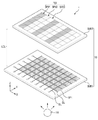
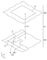
도 2는 도 1의 표시 장치의 임의의 화소들의 레이아웃이다.
도 3은 도 2의 III-III' 선을 따라 절개한 상부 표시판의 단면도이다.
도 4는 도 3에 도시한 제1 서브 화소를 개략적으로 나타낸 도면이다.
도 5는 일 실시예에 따른 백라이트 유닛의 사시도이다.
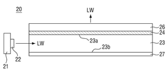
도 6은 도 5의 VI-VI' 선을 따라 절개한 단면도이다.
도 7 및 도 8은 다른 실시예들에 따른 백라이트 유닛의 단면도들이다.
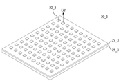
도 9는 또 다른 실시예에 따른 백라이트 유닛의 사시도이다.
도 10a 및 도 10b는 다양한 실시예들에 따른 저굴절층의 단면도들이다.
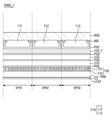
도 11은 일 실시예에 따른 표시 장치의 단면도이다.
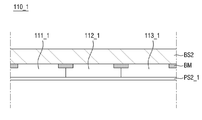
도 12 내지 도 14는 다양한 실시예들에 따른 컬러 필터층의 단면도들이다.
도 15는 또 다른 실시예에 따른 컬러 필터층의 단면도이다.
도 16은 일 실시예에 따른 산란층의 단면도 및 일부 확대도이다.
도 17은 일 실시예에 따른 산란층의 광 산란체 농도에 따른 측면 시인성 향상 효과를 설명하기 위한 그래프이다.
도 18 내지 도 20은 다양한 실시예들에 따른 상부 표시판의 단면도들이다.
도 21은 또 다른 실시예에 따른 표시 장치의 단면도이다.
20: 백라이트 유닛 21: 인쇄 회로 기판
22: 발광 소자 23: 도광판
110: 컬러 필터층 120: 광 산란층
130: 평탄화 유기층 140: 평탄화 레진층
150: 제2 편광층 151: 선 격자 패턴
152: 저반사 금속층 LCL: 액정층
CE: 공통 전극 SPE: 서브 화소 전극
Claims (29)
- 제1 기판;
상기 제1 기판과 대향하는 제2 기판;
상기 제1 기판과 상기 제2 기판 사이에 배치되고, 제1 선 격자 패턴을 포함하는 제1 편광층;
상기 제1 편광층과 상기 제2 기판 사이에 배치된 광 산란층; 및
상기 광 산란층과 상기 제2 기판 사이에 배치된 컬러 필터층을 포함하는 표시 장치. - 제1 항에 있어서,
상기 광 산란층은 유기 물질을 포함하는 베이스층 및 상기 베이스층 내에 분산된 광 산란체를 포함하는 표시 장치. - 제2 항에 있어서,
상기 광 산란체는 TiO2 또는 SiO2를 포함하고, 상기 광 산란체는 상기 광 산란층 100 중량부에 대해 3 내지 11 중량부를 갖는 표시 장치. - 제3 항에 있어서,
상기 광 산란층의 두께는 1um 내지 6um이되, 바람직하게는 3um인 표시 장치. - 제2 항에 있어서,
상기 컬러 필터층은 복수개이고, 이웃하는 상기 컬러 필터층은 서로 이격되어 이격 공간을 형성하는 표시 장치. - 제5 항에 있어서,
상기 제2 기판 상에 배치되고, 상기 이격 공간에 중첩하도록 배치된 블랙 매트릭스를 더 포함하는 표시 장치. - 제6 항에 있어서,
상기 광 산란층은 이웃하는 상기 컬러 필터층 사이의 상기 이격 공간을 충진하는 표시 장치. - 제2 항에 있어서,
상기 컬러 필터층은 복수개이고, 이웃하는 상기 컬러 필터층은 서로 접촉하는 표시 장치. - 제8 항에 있어서,
상기 컬러 필터층과 상기 광 산란층 사이에 배치된 제1 보호층을 더 포함하되, 상기 제1 보호층의 일면은 상기 컬러 필터층과 접촉하고, 상기 제1 보호층의 타면은 상기 광 산란층과 접촉하는 표시 장치. - 제2 항에 있어서,
상기 컬러 필터층은 적색 컬러 필터층, 녹색 컬러 필터층 및 청색 컬러 필터층을 포함하는 표시 장치. - 제2 항에 있어서,
상기 컬러 필터층은 파장 변환 물질을 포함하는 표시 장치. - 제11 항에 있어서,
상기 광 산란층과 상기 제1 편광층 사이에 배치된 평탄화 유기층을 더 포함하는 표시 장치. - 제12 항에 있어서,
상기 평탄화 유기층과 상기 제1 편광층 사이에 배치된 평탄화 레진층을 더 포함하되, 상기 평탄화 유기층은 상기 평탄화 레진층보다 두꺼운 표시 장치. - 제1 항에 있어서,
상기 제1 선 격자 패턴은 알루미늄(Al), 은(Ag), 금(Au), 구리(Cu), 티타늄(Ti), 몰리브덴(Mo), 니켈(Ni) 또는 이들의 합금 중 적어도 하나를 포함하는 표시 장치. - 제14 항에 있어서,
상기 제1 편광층은 상기 제1 선 격자 패턴 상에 배치되는 저반사 금속층을 포함하는 표시 장치. - 제15 항에 있어서,
상기 저반사 금속층은 MoTaOx를 포함하고, 상기 저반사 금속층의 두께는 200Å 내지 400Å인 표시 장치. - 제1 항에 있어서,
상기 제1 기판과 상기 제2 기판 사이에 배치된 액정층을 포함하되, 상기 제1 편광층은 상기 액정층과 상기 제2 기판 사이에 위치하는 표시 장치. - 제17 항에 있어서,
제2 편광층을 더 포함하되, 상기 액정층은 상기 제1 편광층과 상기 제2 편광층 사이에 위치하는 표시 장치. - 제18 항에 있어서,
상기 제2 편광층은 상기 제1 기판과 상기 액정층 사이에 배치되고, 제2 선 격자 패턴을 포함하는 표시 장치. - 제18 항에 있어서,
상기 제1 기판 하부에 배치된 백라이트 유닛을 더 포함하되, 상기 제2 기판은 상기 제1 기판의 상부에 위치하는 표시 장치. - 제20 항에 있어서,
상기 백라이트 유닛은 도광판을 포함하고, 상기 도광판 상에 저굴절층이 접촉하여 배치되는 표시 장치. - 제21 항에 있어서,
상기 광 산란층은 상기 저굴절층과 동일한 물질을 포함하는 표시 장치. - 제1 기판;
상기 제1 기판과 대향하는 제2 기판;
상기 제1 기판과 상기 제2 기판 사이에 배치되고, 제1 선 격자 패턴을 포함하는 제1 편광층;
상기 제1 편광층과 상기 제2 기판 사이에 배치된 광 산란층; 및
상기 광 산란층과 상기 제1 편광층 사이에 배치된 컬러 필터층을 포함하는 표시 장치. - 제23 항에 있어서,
상기 제1 기판과 상기 제2 기판 사이에 배치된 액정층을 포함하되, 상기 제1 편광층은 상기 액정층과 상기 제2 기판 사이에 위치하고, 제2 편광층을 더 포함하되, 상기 액정층은 상기 제1 편광층과 상기 제2 편광층 사이에 위치하는 표시 장치. - 제24 항에 있어서,
상기 광 산란층은 유기 물질을 포함하는 베이스층 및 상기 베이스층 내에 분산된 광 산란체를 포함하고, 상기 광 산란체는 TiO2 또는 SiO2를 포함하고, 상기 광 산란체는 상기 광 산란층 100 중량부에 대해 3 내지 11 중량부를 갖는 표시 장치. - 제25 항에 있어서,
상기 제1 선 격자 패턴은 알루미늄(Al), 은(Ag), 금(Au), 구리(Cu), 티타늄(Ti), 몰리브덴(Mo), 니켈(Ni) 또는 이들의 합금 중 적어도 하나를 포함하고, 상기 제1 편광층은 상기 제1 선 격자 패턴 상에 배치되는 저반사 금속층을 포함하는 표시 장치. - 제1 기판;
상기 제1 기판과 대향하는 제2 기판;
상기 제1 기판과 상기 제2 기판 사이에 배치되고, 제1 선 격자 패턴을 포함하는 제1 편광층;
상기 제1 편광층과 상기 제2 기판 사이에 배치된 컬러 필터층을 포함하되,
상기 컬러 필터층은 광 산란체를 포함하는 표시 장치. - 제27 항에 있어서,
상기 광 산란체는 TiO2 또는 SiO2를 포함하고, 상기 광 산란체는 상기 컬러 필터층 100 중량부에 대해 3 내지 11 중량부를 갖는 표시 장치. - 제28 항에 있어서,
상기 제1 선 격자 패턴은 알루미늄(Al), 은(Ag), 금(Au), 구리(Cu), 티타늄(Ti), 몰리브덴(Mo), 니켈(Ni) 또는 이들의 합금 중 적어도 하나를 포함하고, 상기 제1 편광층은 상기 제1 선 격자 패턴 상에 배치되는 저반사 금속층을 포함하는 표시 장치.
Priority Applications (3)
| Application Number | Priority Date | Filing Date | Title |
|---|---|---|---|
| KR1020180120723A KR102761243B1 (ko) | 2018-10-10 | 2018-10-10 | 표시 장치 |
| US16/507,355 US11500239B2 (en) | 2018-10-10 | 2019-07-10 | Display device |
| CN201910958872.1A CN111025728A (zh) | 2018-10-10 | 2019-10-10 | 显示装置 |
Applications Claiming Priority (1)
| Application Number | Priority Date | Filing Date | Title |
|---|---|---|---|
| KR1020180120723A KR102761243B1 (ko) | 2018-10-10 | 2018-10-10 | 표시 장치 |
Publications (2)
| Publication Number | Publication Date |
|---|---|
| KR20200040980A true KR20200040980A (ko) | 2020-04-21 |
| KR102761243B1 KR102761243B1 (ko) | 2025-02-03 |
Family
ID=70159361
Family Applications (1)
| Application Number | Title | Priority Date | Filing Date |
|---|---|---|---|
| KR1020180120723A Active KR102761243B1 (ko) | 2018-10-10 | 2018-10-10 | 표시 장치 |
Country Status (3)
| Country | Link |
|---|---|
| US (1) | US11500239B2 (ko) |
| KR (1) | KR102761243B1 (ko) |
| CN (1) | CN111025728A (ko) |
Cited By (3)
| Publication number | Priority date | Publication date | Assignee | Title |
|---|---|---|---|---|
| US12235539B2 (en) | 2022-03-11 | 2025-02-25 | Samsung Sdi Co., Ltd. | Liquid crystal display apparatus |
| US12408538B2 (en) | 2021-10-12 | 2025-09-02 | Samsung Display Co., Ltd. | Anti-peeping display device |
| US12578518B2 (en) | 2022-09-23 | 2026-03-17 | Samsung Display Co., Ltd. | Color control member and display device including the same |
Families Citing this family (6)
| Publication number | Priority date | Publication date | Assignee | Title |
|---|---|---|---|---|
| CN118068610A (zh) * | 2019-09-02 | 2024-05-24 | 群创光电股份有限公司 | 电子装置及电子装置的制造方法 |
| KR102905610B1 (ko) * | 2020-03-06 | 2025-12-30 | 삼성디스플레이 주식회사 | 표시 장치 |
| KR20220149877A (ko) * | 2021-04-30 | 2022-11-09 | 삼성디스플레이 주식회사 | 표시 장치 및 그 제조 방법 |
| JP7381911B2 (ja) * | 2021-09-28 | 2023-11-16 | 日亜化学工業株式会社 | 光源及び発光モジュール |
| CN116564198B (zh) * | 2023-05-19 | 2026-03-17 | 安徽熙泰智能科技有限公司 | 显示器眩光改善方法 |
| US12563174B2 (en) * | 2024-03-14 | 2026-02-24 | Liminal Space, Inc. | 3D light emitter with closely spaced packages |
Citations (6)
| Publication number | Priority date | Publication date | Assignee | Title |
|---|---|---|---|---|
| JP2003149642A (ja) * | 2001-11-13 | 2003-05-21 | Matsushita Electric Works Ltd | 液晶用フロントライト |
| KR20140006840A (ko) * | 2011-02-22 | 2014-01-16 | 아사히 가라스 가부시키가이샤 | 미세 구조 성형체 및 그 미세 구조 성형체를 구비한 액정 표시 장치 |
| KR20140060058A (ko) * | 2012-11-09 | 2014-05-19 | 삼성디스플레이 주식회사 | 편광판, 편광판의 제조방법 및 이를 포함하는 표시장치 |
| KR20160084557A (ko) * | 2015-01-05 | 2016-07-14 | 삼성디스플레이 주식회사 | 액정 표시 장치 |
| KR20170050742A (ko) * | 2015-10-30 | 2017-05-11 | 엘지디스플레이 주식회사 | 액정표시장치 |
| KR20170128729A (ko) * | 2016-05-13 | 2017-11-23 | 삼성디스플레이 주식회사 | 표시 장치 |
Family Cites Families (17)
| Publication number | Priority date | Publication date | Assignee | Title |
|---|---|---|---|---|
| KR101201318B1 (ko) * | 2005-12-08 | 2012-11-14 | 엘지디스플레이 주식회사 | 컬러필터기판 및 그 제조방법 |
| US20070242352A1 (en) * | 2006-04-13 | 2007-10-18 | Macmaster Steven William | Wire-grid polarizers, methods of fabrication thereof and their use in transmissive displays |
| KR20080004880A (ko) | 2006-07-07 | 2008-01-10 | 삼성전자주식회사 | 칼라필터 기판, 이를 갖는 표시패널 및 이의 제조방법 |
| KR100917582B1 (ko) * | 2006-08-10 | 2009-09-15 | 주식회사 엘지화학 | 비접촉식 좌표입력 시스템용 도광판을 이용한 비접촉식좌표입력 방법 |
| US8467020B2 (en) * | 2008-04-01 | 2013-06-18 | Sharp Kabushiki Kaisha | Color filter substrate and liquid crystal display device |
| KR20120040413A (ko) * | 2010-10-19 | 2012-04-27 | 엘지이노텍 주식회사 | 와이어 그리드 편광자 및 이를 포함하는 백라이트유닛 |
| TWI502231B (zh) * | 2014-01-06 | 2015-10-01 | Au Optronics Corp | 顯示裝置 |
| CN104698672B (zh) * | 2015-03-03 | 2019-04-09 | 厦门天马微电子有限公司 | 滤色片及其制备方法 |
| KR20170014755A (ko) | 2015-07-31 | 2017-02-08 | 삼성전자주식회사 | 디스플레이 패널 및 이를 포함하는 디스플레이 장치 |
| CN105093646B (zh) * | 2015-08-11 | 2019-03-15 | 京东方科技集团股份有限公司 | 具有无机覆盖层的彩色滤光片基板以及包含它的显示面板 |
| KR102727719B1 (ko) * | 2016-12-20 | 2024-11-08 | 삼성디스플레이 주식회사 | 표시 장치 및 표시 장치의 제조방법 |
| CN106526942B (zh) * | 2017-01-06 | 2018-12-11 | 京东方科技集团股份有限公司 | 显示面板和显示装置 |
| KR102522593B1 (ko) * | 2017-01-19 | 2023-04-17 | 삼성디스플레이 주식회사 | 색변환 표시판 및 이를 포함하는 표시 장치 |
| KR102618811B1 (ko) * | 2017-01-23 | 2023-12-28 | 삼성디스플레이 주식회사 | 색변환 패널 및 이를 포함하는 표시 장치 |
| KR102321892B1 (ko) * | 2017-04-11 | 2021-11-05 | 삼성디스플레이 주식회사 | 표시 장치 및 이의 제조 방법 |
| KR102282060B1 (ko) * | 2017-05-23 | 2021-07-27 | 삼성디스플레이 주식회사 | 표시 장치 및 그 제조 방법 |
| KR102583835B1 (ko) | 2017-06-14 | 2023-10-05 | 삼성디스플레이 주식회사 | 편광층 및 이를 포함하는 표시 장치 |
-
2018
- 2018-10-10 KR KR1020180120723A patent/KR102761243B1/ko active Active
-
2019
- 2019-07-10 US US16/507,355 patent/US11500239B2/en active Active
- 2019-10-10 CN CN201910958872.1A patent/CN111025728A/zh active Pending
Patent Citations (6)
| Publication number | Priority date | Publication date | Assignee | Title |
|---|---|---|---|---|
| JP2003149642A (ja) * | 2001-11-13 | 2003-05-21 | Matsushita Electric Works Ltd | 液晶用フロントライト |
| KR20140006840A (ko) * | 2011-02-22 | 2014-01-16 | 아사히 가라스 가부시키가이샤 | 미세 구조 성형체 및 그 미세 구조 성형체를 구비한 액정 표시 장치 |
| KR20140060058A (ko) * | 2012-11-09 | 2014-05-19 | 삼성디스플레이 주식회사 | 편광판, 편광판의 제조방법 및 이를 포함하는 표시장치 |
| KR20160084557A (ko) * | 2015-01-05 | 2016-07-14 | 삼성디스플레이 주식회사 | 액정 표시 장치 |
| KR20170050742A (ko) * | 2015-10-30 | 2017-05-11 | 엘지디스플레이 주식회사 | 액정표시장치 |
| KR20170128729A (ko) * | 2016-05-13 | 2017-11-23 | 삼성디스플레이 주식회사 | 표시 장치 |
Cited By (3)
| Publication number | Priority date | Publication date | Assignee | Title |
|---|---|---|---|---|
| US12408538B2 (en) | 2021-10-12 | 2025-09-02 | Samsung Display Co., Ltd. | Anti-peeping display device |
| US12235539B2 (en) | 2022-03-11 | 2025-02-25 | Samsung Sdi Co., Ltd. | Liquid crystal display apparatus |
| US12578518B2 (en) | 2022-09-23 | 2026-03-17 | Samsung Display Co., Ltd. | Color control member and display device including the same |
Also Published As
| Publication number | Publication date |
|---|---|
| KR102761243B1 (ko) | 2025-02-03 |
| US20200117046A1 (en) | 2020-04-16 |
| CN111025728A (zh) | 2020-04-17 |
| US11500239B2 (en) | 2022-11-15 |
Similar Documents
| Publication | Publication Date | Title |
|---|---|---|
| KR102761243B1 (ko) | 표시 장치 | |
| US11281045B2 (en) | Color conversion element and display device including the same | |
| US10976599B2 (en) | Backlight unit and display device including the same | |
| KR102579289B1 (ko) | 색변환 소자 및 이를 포함하는 표시 장치 | |
| KR102376594B1 (ko) | 표시 장치 및 그 제조방법 | |
| KR102239112B1 (ko) | 표시장치 | |
| US11029563B2 (en) | Color conversion substrate and related display device | |
| KR102427416B1 (ko) | 표시 장치 및 그 제조 방법 | |
| KR101794653B1 (ko) | 광변환층을 포함한 액정표시패널 및 액정표시장치 | |
| KR20200059369A (ko) | 표시 패널 | |
| US10606123B2 (en) | Display device having a light conversion member and method for fabricating the same | |
| US10725225B2 (en) | Display device | |
| US10663642B2 (en) | Backlight unit, display apparatus including the same and method of manufacturing the same | |
| KR102477574B1 (ko) | 배선 기판, 이를 포함하는 표시 장치 및 배선 기판의 제조 방법 | |
| US12007647B2 (en) | Color conversion panel with improved light efficiency and display device including the same | |
| US10705390B2 (en) | Color conversion substrate and liquid-crystal display device including the same | |
| KR102601483B1 (ko) | 표시 장치 | |
| US20200132914A1 (en) | Backlight unit and display device having the same | |
| US10928576B2 (en) | Optical member and display including the same | |
| US20200012030A1 (en) | Backlight unit and display device including the same | |
| US20200209463A1 (en) | Light guide plate and display device including the same | |
| KR20200084747A (ko) | 도광판 및 이를 포함하는 표시 장치 |
Legal Events
| Date | Code | Title | Description |
|---|---|---|---|
| PA0109 | Patent application |
Patent event code: PA01091R01D Comment text: Patent Application Patent event date: 20181010 |
|
| PG1501 | Laying open of application | ||
| A201 | Request for examination | ||
| PA0201 | Request for examination |
Patent event code: PA02012R01D Patent event date: 20210825 Comment text: Request for Examination of Application Patent event code: PA02011R01I Patent event date: 20181010 Comment text: Patent Application |
|
| E902 | Notification of reason for refusal | ||
| PE0902 | Notice of grounds for rejection |
Comment text: Notification of reason for refusal Patent event date: 20231010 Patent event code: PE09021S01D |
|
| AMND | Amendment | ||
| E601 | Decision to refuse application | ||
| PE0601 | Decision on rejection of patent |
Patent event date: 20240207 Comment text: Decision to Refuse Application Patent event code: PE06012S01D Patent event date: 20231010 Comment text: Notification of reason for refusal Patent event code: PE06011S01I |
|
| X091 | Application refused [patent] | ||
| PX0901 | Re-examination |
Patent event code: PX09011S01I Patent event date: 20240207 Comment text: Decision to Refuse Application Patent event code: PX09012R01I Patent event date: 20231206 Comment text: Amendment to Specification, etc. |
|
| E90F | Notification of reason for final refusal | ||
| PE0902 | Notice of grounds for rejection |
Comment text: Final Notice of Reason for Refusal Patent event date: 20240527 Patent event code: PE09021S02D |
|
| PX0701 | Decision of registration after re-examination |
Patent event date: 20241107 Comment text: Decision to Grant Registration Patent event code: PX07013S01D |
|
| X701 | Decision to grant (after re-examination) | ||
| GRNT | Written decision to grant | ||
| PR0701 | Registration of establishment |
Comment text: Registration of Establishment Patent event date: 20250123 Patent event code: PR07011E01D |
|
| PR1002 | Payment of registration fee |
Payment date: 20250123 End annual number: 3 Start annual number: 1 |
|
| PG1601 | Publication of registration |