KR20200042113A - 디스플레이 장치 - Google Patents
디스플레이 장치 Download PDFInfo
- Publication number
- KR20200042113A KR20200042113A KR1020180122272A KR20180122272A KR20200042113A KR 20200042113 A KR20200042113 A KR 20200042113A KR 1020180122272 A KR1020180122272 A KR 1020180122272A KR 20180122272 A KR20180122272 A KR 20180122272A KR 20200042113 A KR20200042113 A KR 20200042113A
- Authority
- KR
- South Korea
- Prior art keywords
- refractive layer
- pattern
- layer
- refractive
- patterns
- Prior art date
- Legal status (The legal status is an assumption and is not a legal conclusion. Google has not performed a legal analysis and makes no representation as to the accuracy of the status listed.)
- Ceased
Links
Images


Classifications
-
- G—PHYSICS
- G02—OPTICS
- G02B—OPTICAL ELEMENTS, SYSTEMS OR APPARATUS
- G02B6/00—Light guides; Structural details of arrangements comprising light guides and other optical elements, e.g. couplings
- G02B6/0001—Light guides; Structural details of arrangements comprising light guides and other optical elements, e.g. couplings specially adapted for lighting devices or systems
- G02B6/0011—Light guides; Structural details of arrangements comprising light guides and other optical elements, e.g. couplings specially adapted for lighting devices or systems the light guides being planar or of plate-like form
- G02B6/0033—Means for improving the coupling-out of light from the light guide
- G02B6/005—Means for improving the coupling-out of light from the light guide provided by one optical element, or plurality thereof, placed on the light output side of the light guide
- G02B6/0053—Prismatic sheet or layer; Brightness enhancement element, sheet or layer
-
- G—PHYSICS
- G02—OPTICS
- G02F—OPTICAL DEVICES OR ARRANGEMENTS FOR THE CONTROL OF LIGHT BY MODIFICATION OF THE OPTICAL PROPERTIES OF THE MEDIA OF THE ELEMENTS INVOLVED THEREIN; NON-LINEAR OPTICS; FREQUENCY-CHANGING OF LIGHT; OPTICAL LOGIC ELEMENTS; OPTICAL ANALOGUE/DIGITAL CONVERTERS
- G02F1/00—Devices or arrangements for the control of the intensity, colour, phase, polarisation or direction of light arriving from an independent light source, e.g. switching, gating or modulating; Non-linear optics
- G02F1/01—Devices or arrangements for the control of the intensity, colour, phase, polarisation or direction of light arriving from an independent light source, e.g. switching, gating or modulating; Non-linear optics for the control of the intensity, phase, polarisation or colour
- G02F1/13—Devices or arrangements for the control of the intensity, colour, phase, polarisation or direction of light arriving from an independent light source, e.g. switching, gating or modulating; Non-linear optics for the control of the intensity, phase, polarisation or colour based on liquid crystals, e.g. single liquid crystal display cells
- G02F1/133—Constructional arrangements; Operation of liquid crystal cells; Circuit arrangements
- G02F1/1333—Constructional arrangements; Manufacturing methods
- G02F1/1335—Structural association of cells with optical devices, e.g. polarisers or reflectors
- G02F1/133526—Lenses, e.g. microlenses or Fresnel lenses
-
- G—PHYSICS
- G02—OPTICS
- G02F—OPTICAL DEVICES OR ARRANGEMENTS FOR THE CONTROL OF LIGHT BY MODIFICATION OF THE OPTICAL PROPERTIES OF THE MEDIA OF THE ELEMENTS INVOLVED THEREIN; NON-LINEAR OPTICS; FREQUENCY-CHANGING OF LIGHT; OPTICAL LOGIC ELEMENTS; OPTICAL ANALOGUE/DIGITAL CONVERTERS
- G02F1/00—Devices or arrangements for the control of the intensity, colour, phase, polarisation or direction of light arriving from an independent light source, e.g. switching, gating or modulating; Non-linear optics
- G02F1/01—Devices or arrangements for the control of the intensity, colour, phase, polarisation or direction of light arriving from an independent light source, e.g. switching, gating or modulating; Non-linear optics for the control of the intensity, phase, polarisation or colour
- G02F1/13—Devices or arrangements for the control of the intensity, colour, phase, polarisation or direction of light arriving from an independent light source, e.g. switching, gating or modulating; Non-linear optics for the control of the intensity, phase, polarisation or colour based on liquid crystals, e.g. single liquid crystal display cells
- G02F1/133—Constructional arrangements; Operation of liquid crystal cells; Circuit arrangements
- G02F1/1333—Constructional arrangements; Manufacturing methods
- G02F1/1335—Structural association of cells with optical devices, e.g. polarisers or reflectors
-
- G—PHYSICS
- G02—OPTICS
- G02B—OPTICAL ELEMENTS, SYSTEMS OR APPARATUS
- G02B5/00—Optical elements other than lenses
- G02B5/02—Diffusing elements; Afocal elements
- G02B5/0205—Diffusing elements; Afocal elements characterised by the diffusing properties
- G02B5/021—Diffusing elements; Afocal elements characterised by the diffusing properties the diffusion taking place at the element's surface, e.g. by means of surface roughening or microprismatic structures
- G02B5/0231—Diffusing elements; Afocal elements characterised by the diffusing properties the diffusion taking place at the element's surface, e.g. by means of surface roughening or microprismatic structures the surface having microprismatic or micropyramidal shape
-
- G—PHYSICS
- G02—OPTICS
- G02B—OPTICAL ELEMENTS, SYSTEMS OR APPARATUS
- G02B6/00—Light guides; Structural details of arrangements comprising light guides and other optical elements, e.g. couplings
- G02B6/0001—Light guides; Structural details of arrangements comprising light guides and other optical elements, e.g. couplings specially adapted for lighting devices or systems
- G02B6/0011—Light guides; Structural details of arrangements comprising light guides and other optical elements, e.g. couplings specially adapted for lighting devices or systems the light guides being planar or of plate-like form
- G02B6/0033—Means for improving the coupling-out of light from the light guide
- G02B6/005—Means for improving the coupling-out of light from the light guide provided by one optical element, or plurality thereof, placed on the light output side of the light guide
- G02B6/0051—Diffusing sheet or layer
-
- G—PHYSICS
- G02—OPTICS
- G02F—OPTICAL DEVICES OR ARRANGEMENTS FOR THE CONTROL OF LIGHT BY MODIFICATION OF THE OPTICAL PROPERTIES OF THE MEDIA OF THE ELEMENTS INVOLVED THEREIN; NON-LINEAR OPTICS; FREQUENCY-CHANGING OF LIGHT; OPTICAL LOGIC ELEMENTS; OPTICAL ANALOGUE/DIGITAL CONVERTERS
- G02F1/00—Devices or arrangements for the control of the intensity, colour, phase, polarisation or direction of light arriving from an independent light source, e.g. switching, gating or modulating; Non-linear optics
- G02F1/01—Devices or arrangements for the control of the intensity, colour, phase, polarisation or direction of light arriving from an independent light source, e.g. switching, gating or modulating; Non-linear optics for the control of the intensity, phase, polarisation or colour
- G02F1/13—Devices or arrangements for the control of the intensity, colour, phase, polarisation or direction of light arriving from an independent light source, e.g. switching, gating or modulating; Non-linear optics for the control of the intensity, phase, polarisation or colour based on liquid crystals, e.g. single liquid crystal display cells
- G02F1/133—Constructional arrangements; Operation of liquid crystal cells; Circuit arrangements
- G02F1/1333—Constructional arrangements; Manufacturing methods
- G02F1/1335—Structural association of cells with optical devices, e.g. polarisers or reflectors
- G02F1/133502—Antiglare, refractive index matching layers
-
- G—PHYSICS
- G02—OPTICS
- G02F—OPTICAL DEVICES OR ARRANGEMENTS FOR THE CONTROL OF LIGHT BY MODIFICATION OF THE OPTICAL PROPERTIES OF THE MEDIA OF THE ELEMENTS INVOLVED THEREIN; NON-LINEAR OPTICS; FREQUENCY-CHANGING OF LIGHT; OPTICAL LOGIC ELEMENTS; OPTICAL ANALOGUE/DIGITAL CONVERTERS
- G02F1/00—Devices or arrangements for the control of the intensity, colour, phase, polarisation or direction of light arriving from an independent light source, e.g. switching, gating or modulating; Non-linear optics
- G02F1/01—Devices or arrangements for the control of the intensity, colour, phase, polarisation or direction of light arriving from an independent light source, e.g. switching, gating or modulating; Non-linear optics for the control of the intensity, phase, polarisation or colour
- G02F1/13—Devices or arrangements for the control of the intensity, colour, phase, polarisation or direction of light arriving from an independent light source, e.g. switching, gating or modulating; Non-linear optics for the control of the intensity, phase, polarisation or colour based on liquid crystals, e.g. single liquid crystal display cells
- G02F1/133—Constructional arrangements; Operation of liquid crystal cells; Circuit arrangements
- G02F1/1333—Constructional arrangements; Manufacturing methods
- G02F1/1335—Structural association of cells with optical devices, e.g. polarisers or reflectors
- G02F1/133553—Reflecting elements
-
- G—PHYSICS
- G02—OPTICS
- G02F—OPTICAL DEVICES OR ARRANGEMENTS FOR THE CONTROL OF LIGHT BY MODIFICATION OF THE OPTICAL PROPERTIES OF THE MEDIA OF THE ELEMENTS INVOLVED THEREIN; NON-LINEAR OPTICS; FREQUENCY-CHANGING OF LIGHT; OPTICAL LOGIC ELEMENTS; OPTICAL ANALOGUE/DIGITAL CONVERTERS
- G02F1/00—Devices or arrangements for the control of the intensity, colour, phase, polarisation or direction of light arriving from an independent light source, e.g. switching, gating or modulating; Non-linear optics
- G02F1/01—Devices or arrangements for the control of the intensity, colour, phase, polarisation or direction of light arriving from an independent light source, e.g. switching, gating or modulating; Non-linear optics for the control of the intensity, phase, polarisation or colour
- G02F1/13—Devices or arrangements for the control of the intensity, colour, phase, polarisation or direction of light arriving from an independent light source, e.g. switching, gating or modulating; Non-linear optics for the control of the intensity, phase, polarisation or colour based on liquid crystals, e.g. single liquid crystal display cells
- G02F1/133—Constructional arrangements; Operation of liquid crystal cells; Circuit arrangements
- G02F1/1333—Constructional arrangements; Manufacturing methods
- G02F1/1335—Structural association of cells with optical devices, e.g. polarisers or reflectors
- G02F1/13356—Structural association of cells with optical devices, e.g. polarisers or reflectors characterised by the placement of the optical elements
-
- G—PHYSICS
- G02—OPTICS
- G02B—OPTICAL ELEMENTS, SYSTEMS OR APPARATUS
- G02B5/00—Optical elements other than lenses
- G02B5/02—Diffusing elements; Afocal elements
- G02B5/0205—Diffusing elements; Afocal elements characterised by the diffusing properties
- G02B5/0263—Diffusing elements; Afocal elements characterised by the diffusing properties with positional variation of the diffusing properties, e.g. gradient or patterned diffuser
-
- G—PHYSICS
- G02—OPTICS
- G02B—OPTICAL ELEMENTS, SYSTEMS OR APPARATUS
- G02B6/00—Light guides; Structural details of arrangements comprising light guides and other optical elements, e.g. couplings
- G02B6/0001—Light guides; Structural details of arrangements comprising light guides and other optical elements, e.g. couplings specially adapted for lighting devices or systems
- G02B6/0011—Light guides; Structural details of arrangements comprising light guides and other optical elements, e.g. couplings specially adapted for lighting devices or systems the light guides being planar or of plate-like form
- G02B6/0033—Means for improving the coupling-out of light from the light guide
- G02B6/0035—Means for improving the coupling-out of light from the light guide provided on the surface of the light guide or in the bulk of it
- G02B6/0038—Linear indentations or grooves, e.g. arc-shaped grooves or meandering grooves, extending over the full length or width of the light guide
-
- G—PHYSICS
- G02—OPTICS
- G02B—OPTICAL ELEMENTS, SYSTEMS OR APPARATUS
- G02B6/00—Light guides; Structural details of arrangements comprising light guides and other optical elements, e.g. couplings
- G02B6/0001—Light guides; Structural details of arrangements comprising light guides and other optical elements, e.g. couplings specially adapted for lighting devices or systems
- G02B6/0011—Light guides; Structural details of arrangements comprising light guides and other optical elements, e.g. couplings specially adapted for lighting devices or systems the light guides being planar or of plate-like form
- G02B6/0033—Means for improving the coupling-out of light from the light guide
- G02B6/0063—Means for improving the coupling-out of light from the light guide for extracting light out both the major surfaces of the light guide
-
- G—PHYSICS
- G02—OPTICS
- G02F—OPTICAL DEVICES OR ARRANGEMENTS FOR THE CONTROL OF LIGHT BY MODIFICATION OF THE OPTICAL PROPERTIES OF THE MEDIA OF THE ELEMENTS INVOLVED THEREIN; NON-LINEAR OPTICS; FREQUENCY-CHANGING OF LIGHT; OPTICAL LOGIC ELEMENTS; OPTICAL ANALOGUE/DIGITAL CONVERTERS
- G02F1/00—Devices or arrangements for the control of the intensity, colour, phase, polarisation or direction of light arriving from an independent light source, e.g. switching, gating or modulating; Non-linear optics
- G02F1/01—Devices or arrangements for the control of the intensity, colour, phase, polarisation or direction of light arriving from an independent light source, e.g. switching, gating or modulating; Non-linear optics for the control of the intensity, phase, polarisation or colour
- G02F1/13—Devices or arrangements for the control of the intensity, colour, phase, polarisation or direction of light arriving from an independent light source, e.g. switching, gating or modulating; Non-linear optics for the control of the intensity, phase, polarisation or colour based on liquid crystals, e.g. single liquid crystal display cells
- G02F1/133—Constructional arrangements; Operation of liquid crystal cells; Circuit arrangements
- G02F1/1333—Constructional arrangements; Manufacturing methods
- G02F1/1335—Structural association of cells with optical devices, e.g. polarisers or reflectors
- G02F1/13356—Structural association of cells with optical devices, e.g. polarisers or reflectors characterised by the placement of the optical elements
- G02F1/133562—Structural association of cells with optical devices, e.g. polarisers or reflectors characterised by the placement of the optical elements on the viewer side
-
- G02F2001/13356—
-
- G—PHYSICS
- G02—OPTICS
- G02F—OPTICAL DEVICES OR ARRANGEMENTS FOR THE CONTROL OF LIGHT BY MODIFICATION OF THE OPTICAL PROPERTIES OF THE MEDIA OF THE ELEMENTS INVOLVED THEREIN; NON-LINEAR OPTICS; FREQUENCY-CHANGING OF LIGHT; OPTICAL LOGIC ELEMENTS; OPTICAL ANALOGUE/DIGITAL CONVERTERS
- G02F2202/00—Materials and properties
- G02F2202/13—Materials and properties photorefractive
Landscapes
- Physics & Mathematics (AREA)
- Nonlinear Science (AREA)
- General Physics & Mathematics (AREA)
- Optics & Photonics (AREA)
- Mathematical Physics (AREA)
- Chemical & Material Sciences (AREA)
- Crystallography & Structural Chemistry (AREA)
- Planar Illumination Modules (AREA)
- Liquid Crystal (AREA)
- Optical Elements Other Than Lenses (AREA)
Abstract
Description
도 2는 도 1에 도시된 디스플레이 장치를 분해하여 도시한 도면이다.
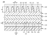
도 3은 도 2에 도시된 광학 필름의 단면을 개략적으로 도시한 도면이다.
도 4는 도 3에 도시된 광학 필름에 입사되는 광이 굴절되는 모습을 개략적으로 도시한 도면이다.
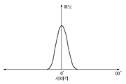
도 5는 도 2에 도시된 백라이트 유닛에서 발산되는 광의 분포를 도시한 그래프이다.
도 6은 본 발명의 다른 실시예에 따른 백라이트 유닛에서 발산되는 광의 분포를 도시한 그래프이다.
도 7은 도 2에 도시된 광학 필름의 제조방법을 도시한 순서도이다.
도 8은 본 발명의 다른 실시예에 따른 광학 필름의 단면을 개략적으로 도시한 도면이다.
도 9는 본 발명의 또 다른 실시예에 따른 광학 필름의 단면을 개략적으로 도시한 도면이다.
도 10은 본 발명의 또 다른 실시예에 따른 광학 필름의 단면을 개략적으로 도시한 도면이다.
20; 디스플레이 패널
60; 백라이트 유닛
100, 200, 300, 400; 광학 필름
101, 201, 301, 401; 기재층
110, 210, 310, 410; 제1 굴절층
112, 212, 312, 412; 제1 패턴
120, 220, 320, 420; 제2 굴절층
130, 230, 330, 430; 제3 굴절층
132, 232, 332, 432; 제2 패턴
140, 240, 340, 440; 제4 굴절층
Claims (20)
- 광을 발산하도록 마련되는 백라이트 유닛;
상기 백라이트 유닛의 전방에 배치되는 디스플레이 패널; 및
상기 디스플레이 패널의 전방에 배치되는 광학 필름;을 포함하며,
상기 광학 필름은,
기재층;
상기 기재층의 전방에 배치되는 제1 굴절층;
상기 제1 굴절층의 전방에 배치되며, 상기 제1 굴절층보다 낮은 굴절률을 갖는 제2 굴절층;
상기 기재층의 후방에 배치되는 제3 굴절층; 및
상기 제3 굴절층의 후방에 배치되며, 상기 제3 굴절층보다 낮은 굴절률을 갖는 제4 굴절층;을 포함하는 디스플레이 장치. - 제1항에 있어서,
상기 제1 굴절층은 상기 백라이트 유닛으로부터 발산된 광의 일부를 전반사시키도록 형성된 제1 경사부를 갖는 제1 패턴을 포함하는 디스플레이 장치. - 제2항에 있어서,
상기 제2 굴절층은 상기 제1 굴절층의 상기 제1 패턴 사이를 충진하는 제1 충진부를 포함하는 디스플레이 장치. - 제2항에 있어서,
상기 제3 굴절층은 상기 제4 굴절층을 통과한 광의 적어도 일부를 굴절시키도록 형성된 제2 경사부를 갖는 제2 패턴을 포함하는 디스플레이 장치. - 제4항에 있어서,
상기 제1 경사부는 상기 제2 경사부보다 큰 경사각을 갖도록 형성되는 디스플레이 장치. - 제4항에 있어서,
상기 제1 패턴은 상기 제2 패턴보다 높은 높이를 갖도록 형성되는 디스플레이 장치. - 제4항에 있어서,
상기 제4 굴절층은 상기 제3 굴절층의 상기 제2 패턴 사이를 충진하는 제2 충진부를 포함하는 디스플레이 장치. - 제4항에 있어서,
상기 제1 패턴 및 상기 제2 패턴은 양각 패턴으로 형성되는 디스플레이 장치. - 제4항에 있어서,
상기 제1 패턴 사이의 간격은 상기 제2 패턴 사이의 간격과 상이하게 마련되는 디스플레이 장치. - 제2항에 있어서,
상기 제1 굴절층의 상기 제1 패턴은 상기 제1 굴절층이 연장되는 방향과 평행하게 연장되는 평행부를 갖는 디스플레이 장치. - 제1항에 있어서,
상기 제1 굴절층은 상기 백라이트 유닛으로부터 발산된 광의 일부를 전반사시키도록 형성된 제1 곡면부를 갖는 제1 패턴을 포함하는 디스플레이 장치. - 제1항에 있어서,
상기 제3 굴절층은 상기 제4 굴절층을 통과한 광의 적어도 일부를 굴절시키도록 형성된 제2 곡면부를 갖는 제2 패턴을 포함하는 디스플레이 장치. - 제12항에 있어서,
상기 제2 패턴은 음각 패턴으로 형성되는 디스플레이 장치. - 디스플레이 패널; 및
상기 디스플레이 패널의 전방에 배치되는 광학 필름;을 포함하며,
상기 광학 필름은,
기재층;
상기 기재층의 전방에 배치되며, 상기 기재층을 통과한 광의 일부를 전반사시키도록 형성되는 제1 경사부를 갖는 제1 패턴이 형성되는 제1 굴절층;
상기 제1 굴절층의 전방에 배치되며, 상기 제1 굴절층보다 낮은 굴절률을 갖는 제2 굴절층;
상기 기재층의 후방에 배치되며, 상기 디스플레이 패널로부터 입사되는 광의 일부를 굴절시키도록 형성되는 제2 경사부를 갖는 제2 패턴이 형성되는 제3 굴절층; 및
상기 제3 굴절층의 후방에 배치되며, 상기 제3 굴절층보다 낮은 굴절률을 갖는 제4 굴절층;을 포함하는 디스플레이 장치. - 제14항에 있어서,
상기 제1 패턴은 양각 패턴으로 형성되며,
상기 제2 굴절층은 상기 제1 패턴 사이를 충진하는 제1 충진부를 포함하는 디스플레이 장치. - 제14항에 있어서,
상기 제2 패턴은 양각 패턴 또는 음각패턴으로 형성되며,
상기 제4 굴절층은 상기 제2 패턴 사이를 충진하는 제2 충진부를 포함하는 디스플레이 장치. - 제14항에 있어서,
상기 제1 경사부는 상기 제2 경사부보다 큰 경사각을 갖도록 형성되는 디스플레이 장치. - 제14항에 있어서,
상기 제1 패턴은 상기 제2 패턴보다 높은 높이를 갖도록 형성되는 디스플레이 장치. - 제14항에 있어서,
상기 제1 패턴 사이의 간격은 상기 제2 패턴 사이의 간격과 상이하게 마련되는 디스플레이 장치. - 디스플레이 패널; 및
상기 디스플레이 패널의 전방에 배치되는 광학 필름;을 포함하며,
상기 광학 필름은,
기재층;
상기 기재층의 전방에 배치되며, 상기 기재층을 통과한 광의 일부를 전반사시키도록 형성되는 제1 경사부를 갖는 제1 패턴이 형성되는 제1 굴절층;
상기 제1 굴절층의 전방에 배치되며, 상기 제1 굴절층보다 낮은 굴절률을 가지고, 상기 제1 패턴 사이를 충진하는 제1 충진부를 포함하는 제2 굴절층;
상기 기재층의 후방에 배치되며, 상기 제1 경사부보다 작은 경사각을 갖도록 형성되는 제2 경사부를 갖는 제2 패턴이 형성되는 제3 굴절층; 및
상기 제3 굴절층의 후방에 배치되며, 상기 제3 굴절층보다 낮은 굴절률을 가지고, 상기 제2 패턴 사이를 충진하는 제2 충진부를 포함하는 제4 굴절층;을 포함하는 디스플레이 장치.
Priority Applications (4)
| Application Number | Priority Date | Filing Date | Title |
|---|---|---|---|
| KR1020180122272A KR20200042113A (ko) | 2018-10-15 | 2018-10-15 | 디스플레이 장치 |
| PCT/KR2019/010943 WO2020080669A1 (en) | 2018-10-15 | 2019-08-27 | Display apparatus |
| EP19200296.2A EP3640720B1 (en) | 2018-10-15 | 2019-09-27 | Display apparatus |
| US16/591,196 US11243342B2 (en) | 2018-10-15 | 2019-10-02 | Display apparatus |
Applications Claiming Priority (1)
| Application Number | Priority Date | Filing Date | Title |
|---|---|---|---|
| KR1020180122272A KR20200042113A (ko) | 2018-10-15 | 2018-10-15 | 디스플레이 장치 |
Publications (1)
| Publication Number | Publication Date |
|---|---|
| KR20200042113A true KR20200042113A (ko) | 2020-04-23 |
Family
ID=68084708
Family Applications (1)
| Application Number | Title | Priority Date | Filing Date |
|---|---|---|---|
| KR1020180122272A Ceased KR20200042113A (ko) | 2018-10-15 | 2018-10-15 | 디스플레이 장치 |
Country Status (4)
| Country | Link |
|---|---|
| US (1) | US11243342B2 (ko) |
| EP (1) | EP3640720B1 (ko) |
| KR (1) | KR20200042113A (ko) |
| WO (1) | WO2020080669A1 (ko) |
Families Citing this family (3)
| Publication number | Priority date | Publication date | Assignee | Title |
|---|---|---|---|---|
| CN115295744B (zh) * | 2020-06-28 | 2025-09-19 | 湖北长江新型显示产业创新中心有限公司 | 显示面板和显示装置 |
| KR102896418B1 (ko) * | 2020-07-01 | 2025-12-09 | 삼성디스플레이 주식회사 | 표시 장치 및 표시 패널 |
| US12554163B2 (en) * | 2021-10-15 | 2026-02-17 | Cm Visual Technology Corporation | Optical film comprising a second optical layer having a plurality of optical portions located in recesses of a first optical layer and display device using the same |
Family Cites Families (15)
| Publication number | Priority date | Publication date | Assignee | Title |
|---|---|---|---|---|
| JP3006306B2 (ja) * | 1992-09-16 | 2000-02-07 | インターナショナル・ビジネス・マシーンズ・コーポレイション | 光学的フイルム及び上記光学的フイルムを用いた液晶表示装置 |
| JP4240037B2 (ja) * | 2003-05-22 | 2009-03-18 | 日立化成工業株式会社 | 光学フィルム及びそれを用いた面光源装置 |
| KR100657914B1 (ko) * | 2004-11-24 | 2006-12-14 | 삼성전자주식회사 | 프리즘 시트 및 이를 채용한 백라이트 유니트 |
| JP2008003232A (ja) * | 2006-06-21 | 2008-01-10 | Fujifilm Corp | 光学シート及び光学シートの製造方法、バックライト、液晶表示装置 |
| KR20080023503A (ko) * | 2006-09-11 | 2008-03-14 | 삼성코닝정밀유리 주식회사 | 광기능성 필름을 포함하는 액정디스플레이장치 및 광기능성필름 |
| WO2008069162A1 (en) * | 2006-12-05 | 2008-06-12 | Semiconductor Energy Laboratory Co., Ltd. | Anti-reflection film and display device |
| US8408775B1 (en) * | 2008-03-12 | 2013-04-02 | Fusion Optix, Inc. | Light recycling directional control element and light emitting device using the same |
| CN102667540A (zh) * | 2009-12-15 | 2012-09-12 | 夏普株式会社 | 光学叠层体、照明装置、液晶显示装置和光学叠层体的制造方法 |
| KR20130046042A (ko) * | 2011-10-27 | 2013-05-07 | 삼성전자주식회사 | 백라이트유닛 및 이를 가지는 디스플레이장치 |
| US10054732B2 (en) * | 2013-02-22 | 2018-08-21 | Reald Spark, Llc | Directional backlight having a rear reflector |
| US9588263B2 (en) * | 2012-08-17 | 2017-03-07 | Corning Incorporated | Display element having buried scattering anti-glare layer |
| KR102301486B1 (ko) * | 2014-12-02 | 2021-09-13 | 삼성디스플레이 주식회사 | 편광 부재 및 이를 포함하는 표시 장치 |
| US20170115433A1 (en) * | 2015-10-21 | 2017-04-27 | Sangbo Corporation | Multilayer optical sheet assembly |
| KR102723297B1 (ko) * | 2016-07-26 | 2024-10-29 | 엘지디스플레이 주식회사 | 디스플레이 장치 |
| KR102399552B1 (ko) * | 2016-11-28 | 2022-05-18 | 삼성전자주식회사 | 백라이트 유닛 및 이를 포함하는 디스플레이 장치 |
-
2018
- 2018-10-15 KR KR1020180122272A patent/KR20200042113A/ko not_active Ceased
-
2019
- 2019-08-27 WO PCT/KR2019/010943 patent/WO2020080669A1/en not_active Ceased
- 2019-09-27 EP EP19200296.2A patent/EP3640720B1/en active Active
- 2019-10-02 US US16/591,196 patent/US11243342B2/en active Active
Also Published As
| Publication number | Publication date |
|---|---|
| US11243342B2 (en) | 2022-02-08 |
| EP3640720B1 (en) | 2023-03-29 |
| WO2020080669A1 (en) | 2020-04-23 |
| US20200117048A1 (en) | 2020-04-16 |
| EP3640720A1 (en) | 2020-04-22 |
Similar Documents
| Publication | Publication Date | Title |
|---|---|---|
| US8687146B2 (en) | Reflective plate and liquid crystal display apparatus having the same | |
| TWI444678B (zh) | 導光板,包含導光板的背光組件,及包含導光板的液晶顯示裝置 | |
| US11054871B2 (en) | Display device including radiant heat blocking layer | |
| US9638956B2 (en) | Backlight unit and display apparatus thereof | |
| CN102563458B (zh) | 背光单元以及包括它的液晶显示器 | |
| KR102188105B1 (ko) | 디스플레이 기기 | |
| US10393938B2 (en) | Display apparatus | |
| CN108614372A (zh) | 液晶显示装置 | |
| KR20100097515A (ko) | 액정표시장치용 백라이트 유닛 | |
| KR20150071437A (ko) | 디스플레이 기기 | |
| US11243342B2 (en) | Display apparatus | |
| CN102610167B (zh) | 显示设备 | |
| EP3599505B1 (en) | Display apparatus | |
| KR101283055B1 (ko) | 백라이트 유닛 및 이를 구비하는 표시장치 | |
| KR101746675B1 (ko) | 복합광학시트 및 이를 포함하는 액정표시장치 | |
| KR102408905B1 (ko) | 디스플레이 장치 | |
| KR20200015110A (ko) | 디스플레이 장치 | |
| US10877204B2 (en) | Illumination device and display apparatus | |
| TWI493255B (zh) | 在用於導光之樹脂層範圍之背光單元以及使用其之lcd | |
| KR102554719B1 (ko) | 발광다이오드 어셈블리와 이를 포함하는 백라이트 유닛 및 이를 포함하는 액정표시장치 | |
| KR20080034702A (ko) | 백라이트유닛과 이를 포함하는 액정표시장치 | |
| KR20200077367A (ko) | 디스플레이 장치 | |
| KR20080060085A (ko) | 백라이트유닛과 이를 포함하는 액정표시장치 | |
| KR20140075356A (ko) | 액정표시장치 | |
| KR20080058619A (ko) | 백라이트유닛과 이를 포함하는 액정표시장치 |
Legal Events
| Date | Code | Title | Description |
|---|---|---|---|
| PA0109 | Patent application |
Patent event code: PA01091R01D Comment text: Patent Application Patent event date: 20181015 |
|
| PG1501 | Laying open of application | ||
| A201 | Request for examination | ||
| PA0201 | Request for examination |
Patent event code: PA02012R01D Patent event date: 20211007 Comment text: Request for Examination of Application Patent event code: PA02011R01I Patent event date: 20181015 Comment text: Patent Application |
|
| E902 | Notification of reason for refusal | ||
| PE0902 | Notice of grounds for rejection |
Comment text: Notification of reason for refusal Patent event date: 20240118 Patent event code: PE09021S01D |
|
| E90F | Notification of reason for final refusal | ||
| PE0902 | Notice of grounds for rejection |
Comment text: Final Notice of Reason for Refusal Patent event date: 20240610 Patent event code: PE09021S02D |
|
| E601 | Decision to refuse application | ||
| E801 | Decision on dismissal of amendment | ||
| PE0601 | Decision on rejection of patent |
Patent event date: 20241210 Comment text: Decision to Refuse Application Patent event code: PE06012S01D |
|
| PE0801 | Dismissal of amendment |
Patent event code: PE08012E01D Comment text: Decision on Dismissal of Amendment Patent event date: 20241210 |