KR20200042555A - 터치 센서 및 표시 장치 - Google Patents
터치 센서 및 표시 장치 Download PDFInfo
- Publication number
- KR20200042555A KR20200042555A KR1020180122358A KR20180122358A KR20200042555A KR 20200042555 A KR20200042555 A KR 20200042555A KR 1020180122358 A KR1020180122358 A KR 1020180122358A KR 20180122358 A KR20180122358 A KR 20180122358A KR 20200042555 A KR20200042555 A KR 20200042555A
- Authority
- KR
- South Korea
- Prior art keywords
- touch
- resistance
- electrode
- touch electrode
- line
- Prior art date
- Legal status (The legal status is an assumption and is not a legal conclusion. Google has not performed a legal analysis and makes no representation as to the accuracy of the status listed.)
- Granted
Links
Images










Classifications
-
- G—PHYSICS
- G06—COMPUTING OR CALCULATING; COUNTING
- G06F—ELECTRIC DIGITAL DATA PROCESSING
- G06F3/00—Input arrangements for transferring data to be processed into a form capable of being handled by the computer; Output arrangements for transferring data from processing unit to output unit, e.g. interface arrangements
- G06F3/01—Input arrangements or combined input and output arrangements for interaction between user and computer
- G06F3/03—Arrangements for converting the position or the displacement of a member into a coded form
- G06F3/041—Digitisers, e.g. for touch screens or touch pads, characterised by the transducing means
- G06F3/0412—Digitisers structurally integrated in a display
-
- G—PHYSICS
- G06—COMPUTING OR CALCULATING; COUNTING
- G06F—ELECTRIC DIGITAL DATA PROCESSING
- G06F3/00—Input arrangements for transferring data to be processed into a form capable of being handled by the computer; Output arrangements for transferring data from processing unit to output unit, e.g. interface arrangements
- G06F3/01—Input arrangements or combined input and output arrangements for interaction between user and computer
- G06F3/03—Arrangements for converting the position or the displacement of a member into a coded form
- G06F3/041—Digitisers, e.g. for touch screens or touch pads, characterised by the transducing means
- G06F3/0414—Digitisers, e.g. for touch screens or touch pads, characterised by the transducing means using force sensing means to determine a position
-
- G—PHYSICS
- G06—COMPUTING OR CALCULATING; COUNTING
- G06F—ELECTRIC DIGITAL DATA PROCESSING
- G06F3/00—Input arrangements for transferring data to be processed into a form capable of being handled by the computer; Output arrangements for transferring data from processing unit to output unit, e.g. interface arrangements
- G06F3/01—Input arrangements or combined input and output arrangements for interaction between user and computer
- G06F3/03—Arrangements for converting the position or the displacement of a member into a coded form
- G06F3/041—Digitisers, e.g. for touch screens or touch pads, characterised by the transducing means
- G06F3/044—Digitisers, e.g. for touch screens or touch pads, characterised by the transducing means by capacitive means
- G06F3/0443—Digitisers, e.g. for touch screens or touch pads, characterised by the transducing means by capacitive means using a single layer of sensing electrodes
-
- G—PHYSICS
- G06—COMPUTING OR CALCULATING; COUNTING
- G06F—ELECTRIC DIGITAL DATA PROCESSING
- G06F3/00—Input arrangements for transferring data to be processed into a form capable of being handled by the computer; Output arrangements for transferring data from processing unit to output unit, e.g. interface arrangements
- G06F3/01—Input arrangements or combined input and output arrangements for interaction between user and computer
- G06F3/03—Arrangements for converting the position or the displacement of a member into a coded form
- G06F3/041—Digitisers, e.g. for touch screens or touch pads, characterised by the transducing means
- G06F3/0416—Control or interface arrangements specially adapted for digitisers
-
- G—PHYSICS
- G06—COMPUTING OR CALCULATING; COUNTING
- G06F—ELECTRIC DIGITAL DATA PROCESSING
- G06F3/00—Input arrangements for transferring data to be processed into a form capable of being handled by the computer; Output arrangements for transferring data from processing unit to output unit, e.g. interface arrangements
- G06F3/01—Input arrangements or combined input and output arrangements for interaction between user and computer
- G06F3/03—Arrangements for converting the position or the displacement of a member into a coded form
- G06F3/041—Digitisers, e.g. for touch screens or touch pads, characterised by the transducing means
- G06F3/044—Digitisers, e.g. for touch screens or touch pads, characterised by the transducing means by capacitive means
-
- G—PHYSICS
- G06—COMPUTING OR CALCULATING; COUNTING
- G06F—ELECTRIC DIGITAL DATA PROCESSING
- G06F3/00—Input arrangements for transferring data to be processed into a form capable of being handled by the computer; Output arrangements for transferring data from processing unit to output unit, e.g. interface arrangements
- G06F3/01—Input arrangements or combined input and output arrangements for interaction between user and computer
- G06F3/03—Arrangements for converting the position or the displacement of a member into a coded form
- G06F3/041—Digitisers, e.g. for touch screens or touch pads, characterised by the transducing means
- G06F3/045—Digitisers, e.g. for touch screens or touch pads, characterised by the transducing means using resistive elements, e.g. a single continuous surface or two parallel surfaces put in contact
-
- H—ELECTRICITY
- H10—SEMICONDUCTOR DEVICES; ELECTRIC SOLID-STATE DEVICES NOT OTHERWISE PROVIDED FOR
- H10K—ORGANIC ELECTRIC SOLID-STATE DEVICES
- H10K59/00—Integrated devices, or assemblies of multiple devices, comprising at least one organic light-emitting element covered by group H10K50/00
- H10K59/10—OLED displays
- H10K59/12—Active-matrix OLED [AMOLED] displays
- H10K59/131—Interconnections, e.g. wiring lines or terminals
-
- H—ELECTRICITY
- H10—SEMICONDUCTOR DEVICES; ELECTRIC SOLID-STATE DEVICES NOT OTHERWISE PROVIDED FOR
- H10K—ORGANIC ELECTRIC SOLID-STATE DEVICES
- H10K59/00—Integrated devices, or assemblies of multiple devices, comprising at least one organic light-emitting element covered by group H10K50/00
- H10K59/40—OLEDs integrated with touch screens
-
- H—ELECTRICITY
- H10—SEMICONDUCTOR DEVICES; ELECTRIC SOLID-STATE DEVICES NOT OTHERWISE PROVIDED FOR
- H10K—ORGANIC ELECTRIC SOLID-STATE DEVICES
- H10K59/00—Integrated devices, or assemblies of multiple devices, comprising at least one organic light-emitting element covered by group H10K50/00
- H10K59/80—Constructional details
- H10K59/87—Passivation; Containers; Encapsulations
- H10K59/873—Encapsulations
-
- H—ELECTRICITY
- H10—SEMICONDUCTOR DEVICES; ELECTRIC SOLID-STATE DEVICES NOT OTHERWISE PROVIDED FOR
- H10K—ORGANIC ELECTRIC SOLID-STATE DEVICES
- H10K77/00—Constructional details of devices covered by this subclass and not covered by groups H10K10/80, H10K30/80, H10K50/80 or H10K59/80
- H10K77/10—Substrates, e.g. flexible substrates
-
- G—PHYSICS
- G06—COMPUTING OR CALCULATING; COUNTING
- G06F—ELECTRIC DIGITAL DATA PROCESSING
- G06F2203/00—Indexing scheme relating to G06F3/00 - G06F3/048
- G06F2203/041—Indexing scheme relating to G06F3/041 - G06F3/045
- G06F2203/04105—Pressure sensors for measuring the pressure or force exerted on the touch surface without providing the touch position
-
- G—PHYSICS
- G06—COMPUTING OR CALCULATING; COUNTING
- G06F—ELECTRIC DIGITAL DATA PROCESSING
- G06F2203/00—Indexing scheme relating to G06F3/00 - G06F3/048
- G06F2203/041—Indexing scheme relating to G06F3/041 - G06F3/045
- G06F2203/04106—Multi-sensing digitiser, i.e. digitiser using at least two different sensing technologies simultaneously or alternatively, e.g. for detecting pen and finger, for saving power or for improving position detection
-
- G—PHYSICS
- G06—COMPUTING OR CALCULATING; COUNTING
- G06F—ELECTRIC DIGITAL DATA PROCESSING
- G06F2203/00—Indexing scheme relating to G06F3/00 - G06F3/048
- G06F2203/041—Indexing scheme relating to G06F3/041 - G06F3/045
- G06F2203/04111—Cross over in capacitive digitiser, i.e. details of structures for connecting electrodes of the sensing pattern where the connections cross each other, e.g. bridge structures comprising an insulating layer, or vias through substrate
-
- G—PHYSICS
- G06—COMPUTING OR CALCULATING; COUNTING
- G06F—ELECTRIC DIGITAL DATA PROCESSING
- G06F2203/00—Indexing scheme relating to G06F3/00 - G06F3/048
- G06F2203/041—Indexing scheme relating to G06F3/041 - G06F3/045
- G06F2203/04113—Peripheral electrode pattern in resistive digitisers, i.e. electrodes at the periphery of the resistive sheet are shaped in patterns enhancing linearity of induced field
-
- G—PHYSICS
- G06—COMPUTING OR CALCULATING; COUNTING
- G06F—ELECTRIC DIGITAL DATA PROCESSING
- G06F3/00—Input arrangements for transferring data to be processed into a form capable of being handled by the computer; Output arrangements for transferring data from processing unit to output unit, e.g. interface arrangements
- G06F3/01—Input arrangements or combined input and output arrangements for interaction between user and computer
- G06F3/03—Arrangements for converting the position or the displacement of a member into a coded form
- G06F3/041—Digitisers, e.g. for touch screens or touch pads, characterised by the transducing means
- G06F3/0414—Digitisers, e.g. for touch screens or touch pads, characterised by the transducing means using force sensing means to determine a position
- G06F3/04144—Digitisers, e.g. for touch screens or touch pads, characterised by the transducing means using force sensing means to determine a position using an array of force sensing means
-
- G—PHYSICS
- G06—COMPUTING OR CALCULATING; COUNTING
- G06F—ELECTRIC DIGITAL DATA PROCESSING
- G06F3/00—Input arrangements for transferring data to be processed into a form capable of being handled by the computer; Output arrangements for transferring data from processing unit to output unit, e.g. interface arrangements
- G06F3/01—Input arrangements or combined input and output arrangements for interaction between user and computer
- G06F3/03—Arrangements for converting the position or the displacement of a member into a coded form
- G06F3/041—Digitisers, e.g. for touch screens or touch pads, characterised by the transducing means
- G06F3/0416—Control or interface arrangements specially adapted for digitisers
- G06F3/04164—Connections between sensors and controllers, e.g. routing lines between electrodes and connection pads
-
- G—PHYSICS
- G06—COMPUTING OR CALCULATING; COUNTING
- G06F—ELECTRIC DIGITAL DATA PROCESSING
- G06F3/00—Input arrangements for transferring data to be processed into a form capable of being handled by the computer; Output arrangements for transferring data from processing unit to output unit, e.g. interface arrangements
- G06F3/01—Input arrangements or combined input and output arrangements for interaction between user and computer
- G06F3/03—Arrangements for converting the position or the displacement of a member into a coded form
- G06F3/041—Digitisers, e.g. for touch screens or touch pads, characterised by the transducing means
- G06F3/044—Digitisers, e.g. for touch screens or touch pads, characterised by the transducing means by capacitive means
- G06F3/0446—Digitisers, e.g. for touch screens or touch pads, characterised by the transducing means by capacitive means using a grid-like structure of electrodes in at least two directions, e.g. using row and column electrodes
Landscapes
- Engineering & Computer Science (AREA)
- General Engineering & Computer Science (AREA)
- Theoretical Computer Science (AREA)
- Human Computer Interaction (AREA)
- Physics & Mathematics (AREA)
- General Physics & Mathematics (AREA)
- Microelectronics & Electronic Packaging (AREA)
- Position Input By Displaying (AREA)
- Measurement Of Length, Angles, Or The Like Using Electric Or Magnetic Means (AREA)
- Electroluminescent Light Sources (AREA)
Abstract
Description
도 2는 도 1에 도시된 터치 센서의 예시적인 블록도이다.
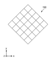
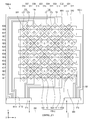
도 3은 도 2의 터치 센서를 도시한 도면으로서, 터치 센서 중 센서부의 평면도 및 센서부와 제어부 간의 연결관계를 도시한 도면이다.
도 4는 도 3의 Q1부분을 확대한 평면도이다.
도 5는 도 4에 도시된 센서부 중 제1층의 구조를 도시한 도면이다.
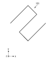
도 6은 도 5의 Q2부분을 확대한 평면도이다.
도 7 및 도 8은 각각 도 6에 도시된 저항선의 변형예를 도시한 것이다.
도 9는 도 6에 도시된 구조의 변형예를 도시한 것이다.
도 10은 도 6의 Q3부분을 확대한 평면도이다.
도 11은 도 4에 도시된 센서부 중 제2층의 구조를 도시한 도면이다.
도 12는 도 4의 X1-X1'를 따라 절단한 단면도이다.
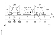
도 13은 도 4의 X2-X2'를 따라 절단한 단면도이다.
도 14는 도 4의 X3-X3'를 따라 절단한 단면도이다.
도 15는 도 12의 변형구조를 도시한 단면도이다.
도 16은 도 13의 변형구조를 도시한 단면도이다.
도 17은 도 14의 변형구조를 도시한 단면도이다.
도 18은 도 6의 Q4부분을 확대한 평면도이다.
도 19는 도 18의 X4-X4'를 따라 절단한 센서부 및 표시패널의 예시적 단면도이다.
도 20은 일 실시예에 따른 터치 센서의 터치 위치 검출동작을 설명하기 위한 도면이다.
도 21은 도 3에 도시된 스트레인 게이지, 제1신호선 및 제2신호선의 배치 와 휘트스톤 브리지 회로부와의 연결관계를 개략적으로 도시한 평면도이다.
도 22는 일 실시예에 따른 터치 센서의 터치 압력 검출동작을 설명하기 위한 도면으로서, 보다 구체적으로 도 21에 도시된 스트레인 게이지와 전기적으로 연결된 휘트스톤 브리지 회로부를 도시한 도면이다.
도 23은 다른 실시예에 따른 터치 센서의 센서부의 평면도 및 센서부와 제어부 간의 연결관계를 도시한 도면이다.
도 24는 또 다른 실시예에 따른 터치 센서의 센서부의 평면도 및 센서부와 제어부 간의 연결관계를 도시한 도면이다.
도 25는 도 24의 Q5부분을 확대한 도면이다.
도 26은 도 25에 도시된 센서부 중 제1층의 구조를 도시한 도면이다.
도 27은 도 25에 도시된 센서부 중 제2층의 구조를 도시한 도면이다.
도 28은 도 25의 X11-X11'를 따라 절단한 단면도이다.
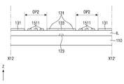
도 29는 도 25의 X12-X12'를 따라 절단한 단면도이다.
도 30은 도 25의 X13-X13'를 따라 절단한 단면도이다.
도 31은 도 25의 X14-X14'를 따라 절단한 단면도이다.
도 32는 도 28의 변형구조를 도시한 단면도이다.
도 33은 도 29의 변형구조를 도시한 단면도이다.
도 34는 도 30의 변형구조를 도시한 단면도이다.
도 35는 도 31의 변형구조를 도시한 단면도이다.
도 36은 또 다른 실시예에 따른 터치 센서의 센서부의 평면도 및 센서부와 제어부 간의 연결관계를 도시한 도면이다.
도 37은 도 36의 Q6부분을 확대한 도면이다.
도 38은 도 37에 도시된 센서부 중 제1층의 구조를 도시한 도면이다.
도 39는 도 37에 도시된 센서부 중 제2층의 구조를 도시한 도면이다.
도 40은 도 37의 X21-X21'를 따라 절단한 단면도이다.
도 41은 도 37의 X22-X22'를 따라 절단한 단면도이다.
도 42는 도 40의 변형구조를 도시한 단면도이다.
도 43은 도 41의 변형구조를 도시한 단면도이다.
도 44는 또 다른 실시예에 따른 터치 센서의 센서부의 평면도 및 센서부와 제어부 간의 연결관계를 도시한 도면이다.
Claims (30)
- 베이스층;
상기 베이스층 상에 제1방향을 따라 배열되고 각각이 제1개구부를 포함하고 상기 제1방향을 따라 서로 전기적으로 연결된 복수의 제1터치전극을 포함하는 제1터치전극부로서,
상기 제1방향과 교차하는 제2방향을 따라 서로 이격되고 복수개 배치된 제1터치전극부;
상기 베이스층 상에 상기 제2방향을 따라 배열되고 상기 제2방향을 따라 서로 전기적으로 연결된 복수의 제2터치전극을 포함하는 제2터치전극부; 및
상기 제1방향을 따라 서로 전기적으로 연결된 복수의 저항선을 포함하는 스트레인 게이지; 를 포함하고,
각각의 상기 저항선은 상기 제1개구부 내에 위치하고,
상기 복수의 저항선 중 상기 제2방향을 따라 이웃하는 두개의 저항선은 서로 전기적으로 연결된 터치 센서. - 제1항에 있어서,
상기 복수의 저항선은 모두 직렬로 연결된 터치센서. - 제1항에 있어서,
상기 복수의 저항선 중 상기 제1터치전극부가 위치하는 임의의 제1전극행의 일단 측에 위치하는 저항선과 상기 제1전극행과 상기 제2방향을 따라 인접한 제2전극행의 일단 측에 위치하는 저항선은 서로 전기적으로 연결된 터치센서. - 제3항에 있어서,
상기 제1전극행의 일단 측에 위치하는 저항선과 상기 제2전극행의 일단에 위치하는 저항선은 동일한 전극열에 위치하는 터치센서. - 제1항에 있어서,
상기 제1터치전극, 상기 제2터치전극 및 상기 저항선은 서로 동일한 제1층에 위치하고,
상기 제1터치전극, 상기 제2터치전극 및 상기 저항선은 동일한 물질로 이루어진 터치센서. - 제5항에 있어서,
상기 제1터치전극부는 상기 복수의 제1터치전극 중 상기 제1방향을 따라 이웃하는 두개의 제1터치전극을 연결하는 제1연결부를 더 포함하고,
상기 제2터치전극부는 상기 복수의 제2터치전극 중 상기 제2방향을 따라 이웃하는 두개의 제2터치전극을 연결하고 상기 제1연결부와 절연된 제2연결부를 더 포함하고,
상기 스트레인 게이지는, 상기 복수의 저항선 중 동일한 전극행에 위치하고 상기 제1방향을 따라 이웃하는 두개의 저항선과 연결된 제1연결선 및 상기 복수의 저항선 중 서로 다른 전극행에 위치하되, 각 전극행의 일단 측에 위치하고 상기 제2방향을 따라 이웃하는 두개의 저항선과 연결된 제2연결선을 더 포함하고,
상기 제1연결부 및 상기 제2연결부 중 어느 하나는 상기 제1층과 다른 제2층에 위치하고,
상기 제1연결부 및 상기 제2연결부 중 다른 하나는 상기 제1층에 위치하고,
상기 제1연결선 및 상기 제2연결선은 상기 제2층에 위치하는 터치센서. - 제6항에 있어서,
상기 베이스층 상에 위치하는 절연층을 더 포함하고,
상기 제1연결선 및 상기 제2연결선은 상기 베이스층 상에 위치하고,
상기 절연층은 상기 제1연결선 상에 위치하고,
상기 제1터치전극, 상기 제2터치전극 및 상기 저항선은 상기 절연층 상에 위치하고,
상기 절연층은 상기 저항선과 상기 제1연결선 사이에 위치하는 터치센서. - 제1항에 있어서,
상기 제1개구부 내에 위치하고 상기 저항선과 연결되고 서로 이격된 복수의 가지부를 더 포함하고,
상기 가지부는 상기 저항선과 동일한 물질로 이루어진 터치센서. - 제1항에 있어서,
상기 제1터치전극부, 상기 제2터치전극부 및 상기 스트레인 게이지와 연결된 제어부를 더 포함하고,
상기 제어부는,
터치 입력에 응답하여 발생한 상기 제1터치전극과 상기 제2터치전극 사이의 정전용량 변화에 기초하여 상기 터치 입력의 위치를 감지하고, 상기 터치 입력에 응답하여 발생한 상기 스트레인 게이지의 저항값 변화에 기초하여 상기 터치 입력의 압력을 감지하도록 구성된 터치센서. - 제1항에 있어서,
상기 스트레인 게이지와 전기적으로 연결된 휘트스톤 브리지 회로부를 더 포함하는 터치센서. - 제10항에 있어서,
상기 스트레인 게이지의 일단과 상기 휘트스톤 브리지 회로부의 한 부분을 전기적으로 연결하는 제1신호선; 및
상기 스트레인 게이지의 타단과 상기 휘트스톤 브리지 회로부의 다른 부분을 전기적으로 연결하는 제2신호선; 을 더 포함하고,
상기 베이스층에는 상기 제1터치전극, 상기 제2터치전극 및 상기 제1저항선이 위치하는 감지영역 및 상기 감지영역의 주변에 위치하는 주변영역이 정의되고,
상기 제1신호선 및 상기 제2신호선은 상기 주변영역에 위치하고,
상기 제1신호선 및 상기 제2신호선은 모두 상기 감지영역의 일측에 위치하는 터치센서. - 제10항에 있어서,
상기 휘트스톤 브리지 회로부는,
구동전압이 인가되고 상기 스트레인 게이지의 일단과 전기적으로 연결된 제1노드, 기준전압이 인가되는 제2노드, 상기 스트레인 게이지의 타단과 전기적으로 연결된 제1출력노드, 제2출력노드, 상기 제2노드 및 상기 제2출력노드에 연결된 제1저항, 상기 제1노드 및 상기 제2출력노드에 연결된 제2저항, 및 상기 제2노드 및 상기 제1출력노드에 연결된 제3저항을 포함하는 터치센서. - 제12항에 있어서,
터치 입력이 인가되지 않은 상태에서, 상기 스트레인 게이지의 저항값, 상기 제1저항의 저항값, 상기 제2저항의 저항값 및 상기 제3저항의 저항값은 실질적으로 동일한 터치센서. - 제1항에 있어서,
상기 베이스층 상에 위치하는 더미전극을 더 포함하되,
상기 제2터치전극은 제2개구부를 포함하고,
상기 제1터치전극, 상기 제2터치전극 및 상기 저항선은 동일한 제1층에 위치하고,
상기 더미전극은, 상기 제2개구부 내에 상기 제2터치전극과 이격되어 위치하되 상기 제1층에 위치하고,
상기 제1터치전극, 상기 제2터치전극, 상기 저항선 및 상기 더미전극은 서로 동일한 물질로 이루어진 터치센서. - 제14항에 있어서,
상기 제2개구부의 면적은 상기 제1개구부의 면적보다 넓은 터치센서. - 제1항에 있어서,
상기 제2터치전극은 구동전극이고 상기 제1터치전극은 감지전극인 터치센서. - 베이스층;
상기 베이스층 상에 제1방향을 따라 배열되고 상기 제1방향을 따라 서로 전기적으로 연결된 복수의 제1터치전극을 포함하는 제1터치전극부;
상기 베이스층 상에 상기 제2방향을 따라 배열되고 각각이 제1개구부를 포함하고 상기 제1방향과 교차하는 제2방향을 따라 서로 전기적으로 연결된 복수의 제2터치전극을 포함하는 제2터치전극부로서,
각각이 상기 제1방향을 따라 서로 이격되고 복수개 배치된 제2터치전극부; 및
상기 제1방향을 따라 서로 전기적으로 연결된 복수의 저항선을 포함하는 스트레인 게이지; 를 포함하고,
각각의 상기 저항선은 상기 제1개구부 내에 위치하고,
상기 복수의 저항선 중 상기 제2방향을 따라 이웃하는 두개의 제1저항선은 서로 전기적으로 연결된 터치 센서. - 제17항에 있어서,
상기 복수의 저항선은 모두 직렬로 연결된 터치센서. - 제17항에 있어서,
상기 복수의 저항선 중 상기 제2터치전극이 위치하는 임의의 제1행의 일단 측에 위치하는 저항선과 상기 제1행과 상기 제2방향을 따라 인접한 제2행의 일단 측에 위치하는 저항선은 서로 전기적으로 연결된 터치센서. - 제17항에 있어서,
상기 제1터치전극부는 상기 복수의 제1터치전극 중 상기 제1방향을 따라 이웃하는 두개의 제1터치전극을 연결하는 제1연결부를 더 포함하고,
상기 제2터치전극부는 상기 복수의 제2터치전극 중 상기 제2방향을 따라 이웃하는 두개의 제2터치전극을 연결하고 상기 제1연결부와 절연된 제2연결부를 더 포함하고,
상기 제1터치전극 및 상기 제2터치전극은 서로 동일한 제1층에 위치하고,
상기 제1연결부 및 상기 제2연결부 중 어느 하나는 상기 제1층과 다른 제2층에 위치하고,
상기 제1연결부 및 상기 제2연결부 중 다른 하나는 상기 제1층에 위치하고,
상기 저항선은 상기 제1층 또는 상기 제2층에 위치하는 터치센서. - 제20항에 있어서,
상기 저항선은 상기 제1층에 위치하고,
상기 제1터치전극, 상기 제2터치전극 및 상기 저항선은 동일한 물질로 이루어진 터치센서. - 제20항에 있어서,
상기 스트레인 게이지는, 상기 복수의 저항선 중 동일한 전극행에 위치하는 저항선을 서로 전기적으로 연결하는 제1연결선 및 상기 복수의 저항선 중 서로 다른 전극행에 위치하되 각 전극행의 일단 측에 위치하고 상기 제2방향을 따라 이웃하는 두개의 저항선을 서로 전기적으로 연결하는 제2연결선을 더 포함하고,
상기 제1연결선 및 상기 제2연결선은 상기 저항선과 다른 층에 위치하는 터치센서. - 제17항에 있어서,
상기 베이스층 상에 위치하는 더미전극을 더 포함하되,
상기 제1터치전극은 제2개구부를 포함하고,
상기 제1터치전극, 상기 제2터치전극 및 상기 저항선은 동일한 제1층에 위치하고,
상기 더미전극은, 상기 제2개구부 내에 상기 제1터치전극과 이격되어 위치하되 상기 제1층에 위치하고,
상기 제1터치전극, 상기 제2터치전극, 상기 저항선 및 상기 더미전극은 서로 동일한 물질로 이루어진 터치센서. - 베이스층;
상기 베이스층 상에 제1방향을 따라 배열되고 각각이 제1개구부를 포함하고 상기 제1방향을 따라 서로 전기적으로 연결된 복수의 제1터치전극을 포함하는 제1터치전극부로서,
상기 제1방향과 교차하는 제2방향을 따라 서로 이격되고 복수개 배치된 제1터치전극부;
상기 베이스층 상에 상기 제2방향을 따라 배열되고 각각이 제2개구부를 포함하고 상기 제2방향을 따라 서로 전기적으로 연결된 복수의 제2터치전극을 포함하는 제2터치전극부로서,
각각이 상기 제1방향을 따라 서로 이격되고 복수개 배치된 제2터치전극부; 및
상기 제1방향을 따라 서로 전기적으로 연결된 복수의 제1저항선 및 상기 제1방향을 따라 서로 전기적으로 연결된 복수의 제2저항선을 포함하는 스트레인 게이지; 를 포함하고,
각각의 상기 제1저항선은 상기 제1개구부 내에 위치하되 상기 제1터치전극과 이격되고,
각각의 상기 제2저항선은 상기 제2개구부 내에 위치하되 상기 제2터치전극과 이격되고,
상기 복수의 제1저항선 중 어느 하나와 상기 복수의 제2저항선 중 어느 하나는 상기 제2방향을 따라 이웃하고 서로 전기적으로 연결된 터치 센서. - 제24항에 있어서,
상기 제1터치전극, 상기 제2터치전극, 상기 제1저항선 및 상기 제2저항선은 동일한 층에 위치하고,
상기 제1터치전극, 상기 제2터치전극, 상기 제1저항선 및 상기 제2저항선은 동일한 물질로 이루어진 터치센서. - 제24항에 있어서,
상기 제2저항선의 길이는 상기 제1저항선의 길이와 다른 터치센서. - 제26항에 있어서,
상기 제2개구부의 면적은 상기 제1개구부의 면적보다 넓고,
상기 제2저항선의 길이는 상기 제1저항선의 길이보다 긴 터치센서. - 제24항에 있어서,
상기 스트레인 게이지는,
상기 복수의 제1저항선 중 임의의 전극행의 일단 측에 위치하는 제1저항선 및 상기 복수의 제2저항선 중 상기 임의의 전극행과 제2방향을 따라 인접한 행의 일단 측에 위치하는 제2저항선과 연결된 연결선을 더 포함하고,
상기 연결선은 상기 제1터치전극 및 상기 제2터치전극과 다른 층에 위치하는 터치센서. - 베이스 기판;
상기 베이스 기판 상에 위치하는 발광소자;
상기 발광소자 상에 위치하는 박막 봉지층;
상기 박막 봉지층 상에 위치하고 개구부를 포함하는 복수의 터치전극; 및
각각이 상기 개구부 내에 위치하되 상기 터치전극과 동일한 층에 위치하고 터치 입력에 응답하여 저항값이 변화하는 저항선과, 상기 저항선 중 제1방향을 따라 이웃하는 두개의 저항선과 연결된 제1연결선과, 상기 저항선 중 상기 제1방향과 교차하는 제2방향을 따라 이웃하는 두개의 저항선과 연결된 제2연결선을 포함하는 스트레인 게이지; 를 포함하고,
상기 제1연결선 및 상기 제2연결선은 상기 박막 봉지층과 상기 저항선 사이에 위치하는 표시장치. - 제29항에 있어서,
상기 박막 봉지층은,
상기 발광소자 상에 위치하는 제1봉지 무기막,
상기 제1봉지 무기막 상에 위치하는 봉지 유기막, 및
상기 봉지 유기막 상에 위치하는 제2봉지 무기막을 포함하고,
상기 터치전극 및 상기 스트레인 게이지는 상기 제2봉지 무기막 상에 위치하는 표시장치.
Priority Applications (8)
| Application Number | Priority Date | Filing Date | Title |
|---|---|---|---|
| KR1020180122358A KR102647742B1 (ko) | 2018-10-15 | 2018-10-15 | 터치 센서 및 표시 장치 |
| US16/560,318 US10908723B2 (en) | 2018-10-15 | 2019-09-04 | Touch sensor and display device |
| CN201910950587.5A CN111045543B (zh) | 2018-10-15 | 2019-10-08 | 触摸传感器和显示装置 |
| EP19202843.9A EP3647919A3 (en) | 2018-10-15 | 2019-10-11 | Touch sensor |
| US17/161,576 US11307699B2 (en) | 2018-10-15 | 2021-01-28 | Touch sensor having strain gauge and display device including the same |
| US17/723,344 US11703969B2 (en) | 2018-10-15 | 2022-04-18 | Touch sensor having strain gauge and display device including the same |
| US18/211,282 US12086340B2 (en) | 2018-10-15 | 2023-06-18 | Touch sensor having strain gauge and display device including the same |
| KR1020240033830A KR102809731B1 (ko) | 2018-10-15 | 2024-03-11 | 터치 센서 및 표시 장치 |
Applications Claiming Priority (1)
| Application Number | Priority Date | Filing Date | Title |
|---|---|---|---|
| KR1020180122358A KR102647742B1 (ko) | 2018-10-15 | 2018-10-15 | 터치 센서 및 표시 장치 |
Related Child Applications (1)
| Application Number | Title | Priority Date | Filing Date |
|---|---|---|---|
| KR1020240033830A Division KR102809731B1 (ko) | 2018-10-15 | 2024-03-11 | 터치 센서 및 표시 장치 |
Publications (2)
| Publication Number | Publication Date |
|---|---|
| KR20200042555A true KR20200042555A (ko) | 2020-04-24 |
| KR102647742B1 KR102647742B1 (ko) | 2024-03-14 |
Family
ID=68280899
Family Applications (2)
| Application Number | Title | Priority Date | Filing Date |
|---|---|---|---|
| KR1020180122358A Active KR102647742B1 (ko) | 2018-10-15 | 2018-10-15 | 터치 센서 및 표시 장치 |
| KR1020240033830A Active KR102809731B1 (ko) | 2018-10-15 | 2024-03-11 | 터치 센서 및 표시 장치 |
Family Applications After (1)
| Application Number | Title | Priority Date | Filing Date |
|---|---|---|---|
| KR1020240033830A Active KR102809731B1 (ko) | 2018-10-15 | 2024-03-11 | 터치 센서 및 표시 장치 |
Country Status (4)
| Country | Link |
|---|---|
| US (4) | US10908723B2 (ko) |
| EP (1) | EP3647919A3 (ko) |
| KR (2) | KR102647742B1 (ko) |
| CN (1) | CN111045543B (ko) |
Cited By (1)
| Publication number | Priority date | Publication date | Assignee | Title |
|---|---|---|---|---|
| KR20240013265A (ko) * | 2021-03-26 | 2024-01-30 | 주식회사 하이딥 | 터치 입력 장치 |
Families Citing this family (11)
| Publication number | Priority date | Publication date | Assignee | Title |
|---|---|---|---|---|
| CN107992239B (zh) * | 2017-11-24 | 2020-06-26 | 合肥鑫晟光电科技有限公司 | 触控基板及其制造方法、显示装置 |
| KR102647742B1 (ko) * | 2018-10-15 | 2024-03-14 | 삼성디스플레이 주식회사 | 터치 센서 및 표시 장치 |
| US11119612B2 (en) * | 2019-02-27 | 2021-09-14 | Wuhan China Star Optoelectronics Semiconductor Display Technology Co., Ltd. | Embedded touch panel with touch drive lines structure that improves sensitivity |
| KR102710197B1 (ko) * | 2019-04-01 | 2024-09-26 | 삼성디스플레이 주식회사 | 압력 센서를 갖는 터치 감지 유닛과 그를 포함하는 표시 장치 |
| CN111766978B (zh) * | 2020-06-12 | 2021-09-24 | 深圳市华星光电半导体显示技术有限公司 | 触控组件及触控显示装置 |
| US12153471B2 (en) * | 2020-09-30 | 2024-11-26 | Google Llc | System and method for detecting faults in foldable glass |
| CN112490229B (zh) * | 2020-11-30 | 2022-08-09 | 湖北长江新型显示产业创新中心有限公司 | 一种显示面板及显示装置 |
| KR102499519B1 (ko) * | 2021-09-17 | 2023-02-16 | 주식회사 하이딥 | 터치 센서 및 이를 포함하는 터치 입력 장치 |
| TWI821079B (zh) * | 2022-12-21 | 2023-11-01 | 友達光電股份有限公司 | 壓力感測器 |
| TWI841197B (zh) | 2023-01-17 | 2024-05-01 | 元太科技工業股份有限公司 | 觸控面板與電子裝置 |
| TWI902016B (zh) * | 2023-09-23 | 2025-10-21 | 友達光電股份有限公司 | 顯示模組 |
Citations (6)
| Publication number | Priority date | Publication date | Assignee | Title |
|---|---|---|---|---|
| US20100128002A1 (en) * | 2008-11-26 | 2010-05-27 | William Stacy | Touch-sensitive display method and apparatus |
| US20160195955A1 (en) * | 2015-01-07 | 2016-07-07 | Microsoft Technology Licensing, Llc | Combined Sensor System |
| US20170010730A1 (en) * | 2015-07-10 | 2017-01-12 | Tpk Touch Solutions (Xiamen) Inc. | Touch display module having pressure detection mechanism and driving method of the same |
| KR20170063216A (ko) * | 2015-11-30 | 2017-06-08 | 엘지디스플레이 주식회사 | 유기발광 표시장치와 그의 제조방법 |
| US20170285799A1 (en) * | 2016-03-29 | 2017-10-05 | Japan Display Inc. | Detecting apparatus and display apparatus |
| KR20180033353A (ko) * | 2016-09-23 | 2018-04-03 | 삼성디스플레이 주식회사 | 표시 장치 및 이의 제조 방법 |
Family Cites Families (27)
| Publication number | Priority date | Publication date | Assignee | Title |
|---|---|---|---|---|
| US20080309633A1 (en) * | 2007-06-13 | 2008-12-18 | Apple Inc. | Touch-sensitive display |
| TWI367437B (en) * | 2007-09-29 | 2012-07-01 | Au Optronics Corp | Touch panel and manufacturing method thereof |
| JP4945483B2 (ja) * | 2008-02-27 | 2012-06-06 | 株式会社 日立ディスプレイズ | 表示パネル |
| JP4720857B2 (ja) * | 2008-06-18 | 2011-07-13 | ソニー株式会社 | 静電容量型入力装置および入力機能付き表示装置 |
| JP2012178093A (ja) * | 2011-02-28 | 2012-09-13 | Japan Display East Co Ltd | タッチパネル装置 |
| US8780074B2 (en) * | 2011-07-06 | 2014-07-15 | Sharp Kabushiki Kaisha | Dual-function transducer for a touch panel |
| US8988384B2 (en) * | 2011-09-23 | 2015-03-24 | Apple Inc. | Force sensor interface for touch controller |
| KR20130035763A (ko) * | 2011-09-30 | 2013-04-09 | 삼성전자주식회사 | 터치 스크린 패널 |
| US9459160B2 (en) * | 2012-06-13 | 2016-10-04 | Microsoft Technology Licensing, Llc | Input device sensor configuration |
| US9158407B2 (en) * | 2012-08-29 | 2015-10-13 | Sharp Kabushiki Kaisha | Capacitive touch panel with a ‘dual layer’ force sensor |
| TWI498797B (zh) * | 2012-12-13 | 2015-09-01 | Au Optronics Corp | 觸控面板及觸控顯示面板 |
| KR102058699B1 (ko) * | 2013-01-24 | 2019-12-26 | 삼성디스플레이 주식회사 | 터치 및 휨 감지 기능을 가지는 플렉서블 표시장치 |
| TWI521288B (zh) * | 2013-03-07 | 2016-02-11 | 友達光電股份有限公司 | 一種觸控單元陣列以及觸控顯示面板 |
| GB2525174A (en) | 2014-04-14 | 2015-10-21 | Nokia Technologies Oy | An apparatus and method for sensing |
| CN106293290B (zh) * | 2015-06-10 | 2023-08-29 | 宸鸿科技(厦门)有限公司 | 触控装置 |
| CN106325579B (zh) | 2015-07-10 | 2023-04-07 | 宸鸿科技(厦门)有限公司 | 一种压力感测输入装置 |
| CN105677111B (zh) | 2016-01-29 | 2020-07-07 | 上海天马微电子有限公司 | 一种阵列基板及显示面板 |
| CN105677112B (zh) * | 2016-02-24 | 2019-01-18 | 上海天马微电子有限公司 | 触控显示面板和触控显示装置 |
| US10691245B2 (en) | 2016-06-22 | 2020-06-23 | Samsung Display Co., Ltd. | Touch sensor |
| KR102558365B1 (ko) * | 2016-09-20 | 2023-07-21 | 삼성디스플레이 주식회사 | 터치 센서 및 이를 포함하는 표시 장치 |
| CN106648200B (zh) * | 2016-09-23 | 2019-03-29 | 上海天马微电子有限公司 | 一种oled阵列基板、显示面板及显示装置 |
| KR101958323B1 (ko) | 2016-11-22 | 2019-03-15 | 주식회사 하이딥 | 압력 감지부 및 이를 포함하는 터치 입력 장치 |
| CN106803513B (zh) * | 2017-01-03 | 2019-07-12 | 上海天马微电子有限公司 | 一种触摸传感器及其制作方法、触摸显示面板 |
| KR102811755B1 (ko) | 2017-02-03 | 2025-05-23 | 삼성디스플레이 주식회사 | 터치 센서 및 이를 구비한 디스플레이 장치 |
| KR102449984B1 (ko) * | 2017-10-31 | 2022-10-05 | 엘지디스플레이 주식회사 | 터치센서를 포함하는 표시장치 및 그의 제조방법 |
| KR102521058B1 (ko) | 2018-05-18 | 2023-04-12 | 삼성디스플레이 주식회사 | 터치 센서 및 표시 장치 |
| KR102647742B1 (ko) * | 2018-10-15 | 2024-03-14 | 삼성디스플레이 주식회사 | 터치 센서 및 표시 장치 |
-
2018
- 2018-10-15 KR KR1020180122358A patent/KR102647742B1/ko active Active
-
2019
- 2019-09-04 US US16/560,318 patent/US10908723B2/en active Active
- 2019-10-08 CN CN201910950587.5A patent/CN111045543B/zh active Active
- 2019-10-11 EP EP19202843.9A patent/EP3647919A3/en active Pending
-
2021
- 2021-01-28 US US17/161,576 patent/US11307699B2/en active Active
-
2022
- 2022-04-18 US US17/723,344 patent/US11703969B2/en active Active
-
2023
- 2023-06-18 US US18/211,282 patent/US12086340B2/en active Active
-
2024
- 2024-03-11 KR KR1020240033830A patent/KR102809731B1/ko active Active
Patent Citations (6)
| Publication number | Priority date | Publication date | Assignee | Title |
|---|---|---|---|---|
| US20100128002A1 (en) * | 2008-11-26 | 2010-05-27 | William Stacy | Touch-sensitive display method and apparatus |
| US20160195955A1 (en) * | 2015-01-07 | 2016-07-07 | Microsoft Technology Licensing, Llc | Combined Sensor System |
| US20170010730A1 (en) * | 2015-07-10 | 2017-01-12 | Tpk Touch Solutions (Xiamen) Inc. | Touch display module having pressure detection mechanism and driving method of the same |
| KR20170063216A (ko) * | 2015-11-30 | 2017-06-08 | 엘지디스플레이 주식회사 | 유기발광 표시장치와 그의 제조방법 |
| US20170285799A1 (en) * | 2016-03-29 | 2017-10-05 | Japan Display Inc. | Detecting apparatus and display apparatus |
| KR20180033353A (ko) * | 2016-09-23 | 2018-04-03 | 삼성디스플레이 주식회사 | 표시 장치 및 이의 제조 방법 |
Cited By (1)
| Publication number | Priority date | Publication date | Assignee | Title |
|---|---|---|---|---|
| KR20240013265A (ko) * | 2021-03-26 | 2024-01-30 | 주식회사 하이딥 | 터치 입력 장치 |
Also Published As
| Publication number | Publication date |
|---|---|
| EP3647919A3 (en) | 2020-07-29 |
| US11703969B2 (en) | 2023-07-18 |
| US20200117305A1 (en) | 2020-04-16 |
| KR102647742B1 (ko) | 2024-03-14 |
| EP3647919A2 (en) | 2020-05-06 |
| US11307699B2 (en) | 2022-04-19 |
| US10908723B2 (en) | 2021-02-02 |
| CN111045543A (zh) | 2020-04-21 |
| US12086340B2 (en) | 2024-09-10 |
| US20220244803A1 (en) | 2022-08-04 |
| CN111045543B (zh) | 2024-04-05 |
| US20210149517A1 (en) | 2021-05-20 |
| US20230333680A1 (en) | 2023-10-19 |
| KR20240038940A (ko) | 2024-03-26 |
| KR102809731B1 (ko) | 2025-05-19 |
Similar Documents
| Publication | Publication Date | Title |
|---|---|---|
| KR102809731B1 (ko) | 터치 센서 및 표시 장치 | |
| US12135857B2 (en) | Touch sensor and display device | |
| KR102700567B1 (ko) | 터치 센서 및 표시 장치 | |
| KR102720520B1 (ko) | 터치 센서 및 표시 장치 | |
| CN111142700B (zh) | 触摸传感器和显示装置 | |
| KR102814675B1 (ko) | 센서 모듈 및 이를 포함하는 표시 장치 | |
| CN111142699B (zh) | 触摸传感器和显示装置 | |
| EP3561649B1 (en) | Touch sensor including touch sensing electrodes |
Legal Events
| Date | Code | Title | Description |
|---|---|---|---|
| PA0109 | Patent application |
Patent event code: PA01091R01D Comment text: Patent Application Patent event date: 20181015 |
|
| PG1501 | Laying open of application | ||
| A201 | Request for examination | ||
| PA0201 | Request for examination |
Patent event code: PA02012R01D Patent event date: 20210923 Comment text: Request for Examination of Application Patent event code: PA02011R01I Patent event date: 20181015 Comment text: Patent Application |
|
| E902 | Notification of reason for refusal | ||
| PE0902 | Notice of grounds for rejection |
Comment text: Notification of reason for refusal Patent event date: 20230703 Patent event code: PE09021S01D |
|
| E701 | Decision to grant or registration of patent right | ||
| PE0701 | Decision of registration |
Patent event code: PE07011S01D Comment text: Decision to Grant Registration Patent event date: 20231212 |
|
| A107 | Divisional application of patent | ||
| GRNT | Written decision to grant | ||
| PA0107 | Divisional application |
Comment text: Divisional Application of Patent Patent event date: 20240311 Patent event code: PA01071R01D |
|
| PR0701 | Registration of establishment |
Comment text: Registration of Establishment Patent event date: 20240311 Patent event code: PR07011E01D |
|
| PR1002 | Payment of registration fee |
Payment date: 20240311 End annual number: 3 Start annual number: 1 |
|
| PG1601 | Publication of registration |