KR20200044992A - 생물학적 응용들을 위한 독립 멤브레인을 생성하는 방법 - Google Patents
생물학적 응용들을 위한 독립 멤브레인을 생성하는 방법 Download PDFInfo
- Publication number
- KR20200044992A KR20200044992A KR1020207011448A KR20207011448A KR20200044992A KR 20200044992 A KR20200044992 A KR 20200044992A KR 1020207011448 A KR1020207011448 A KR 1020207011448A KR 20207011448 A KR20207011448 A KR 20207011448A KR 20200044992 A KR20200044992 A KR 20200044992A
- Authority
- KR
- South Korea
- Prior art keywords
- substrate
- nanopores
- thin film
- forming
- layer
- Prior art date
- Legal status (The legal status is an assumption and is not a legal conclusion. Google has not performed a legal analysis and makes no representation as to the accuracy of the status listed.)
- Granted
Links
Images





Classifications
-
- H—ELECTRICITY
- H10—SEMICONDUCTOR DEVICES; ELECTRIC SOLID-STATE DEVICES NOT OTHERWISE PROVIDED FOR
- H10W—GENERIC PACKAGES, INTERCONNECTIONS, CONNECTORS OR OTHER CONSTRUCTIONAL DETAILS OF DEVICES COVERED BY CLASS H10
- H10W20/00—Interconnections in chips, wafers or substrates
- H10W20/01—Manufacture or treatment
- H10W20/071—Manufacture or treatment of dielectric parts thereof
- H10W20/081—Manufacture or treatment of dielectric parts thereof by forming openings in the dielectric parts
- H10W20/089—Manufacture or treatment of dielectric parts thereof by forming openings in the dielectric parts using processes for implementing desired shapes or dispositions of the openings, e.g. double patterning
-
- G—PHYSICS
- G01—MEASURING; TESTING
- G01N—INVESTIGATING OR ANALYSING MATERIALS BY DETERMINING THEIR CHEMICAL OR PHYSICAL PROPERTIES
- G01N33/00—Investigating or analysing materials by specific methods not covered by groups G01N1/00 - G01N31/00
- G01N33/48—Biological material, e.g. blood, urine; Haemocytometers
- G01N33/483—Physical analysis of biological material
- G01N33/487—Physical analysis of biological material of liquid biological material
- G01N33/48707—Physical analysis of biological material of liquid biological material by electrical means
- G01N33/48721—Investigating individual macromolecules, e.g. by translocation through nanopores
-
- H01L21/76816—
-
- B—PERFORMING OPERATIONS; TRANSPORTING
- B81—MICROSTRUCTURAL TECHNOLOGY
- B81C—PROCESSES OR APPARATUS SPECIALLY ADAPTED FOR THE MANUFACTURE OR TREATMENT OF MICROSTRUCTURAL DEVICES OR SYSTEMS
- B81C1/00—Manufacture or treatment of devices or systems in or on a substrate
- B81C1/00015—Manufacture or treatment of devices or systems in or on a substrate for manufacturing microsystems
- B81C1/00023—Manufacture or treatment of devices or systems in or on a substrate for manufacturing microsystems without movable or flexible elements
- B81C1/00087—Holes
-
- B—PERFORMING OPERATIONS; TRANSPORTING
- B82—NANOTECHNOLOGY
- B82B—NANOSTRUCTURES FORMED BY MANIPULATION OF INDIVIDUAL ATOMS, MOLECULES, OR LIMITED COLLECTIONS OF ATOMS OR MOLECULES AS DISCRETE UNITS; MANUFACTURE OR TREATMENT THEREOF
- B82B1/00—Nanostructures formed by manipulation of individual atoms or molecules, or limited collections of atoms or molecules as discrete units
- B82B1/002—Devices comprising flexible or deformable elements
-
- B—PERFORMING OPERATIONS; TRANSPORTING
- B82—NANOTECHNOLOGY
- B82B—NANOSTRUCTURES FORMED BY MANIPULATION OF INDIVIDUAL ATOMS, MOLECULES, OR LIMITED COLLECTIONS OF ATOMS OR MOLECULES AS DISCRETE UNITS; MANUFACTURE OR TREATMENT THEREOF
- B82B3/00—Manufacture or treatment of nanostructures by manipulation of individual atoms or molecules, or limited collections of atoms or molecules as discrete units
- B82B3/0009—Forming specific nanostructures
- B82B3/0023—Forming specific nanostructures comprising flexible or deformable elements
-
- G—PHYSICS
- G01—MEASURING; TESTING
- G01N—INVESTIGATING OR ANALYSING MATERIALS BY DETERMINING THEIR CHEMICAL OR PHYSICAL PROPERTIES
- G01N27/00—Investigating or analysing materials by the use of electric, electrochemical, or magnetic means
- G01N27/26—Investigating or analysing materials by the use of electric, electrochemical, or magnetic means by investigating electrochemical variables; by using electrolysis or electrophoresis
- G01N27/416—Systems
- G01N27/447—Systems using electrophoresis
- G01N27/44756—Apparatus specially adapted therefor
- G01N27/44791—Microapparatus
-
- H01L21/0226—
-
- H01L21/311—
-
- H01L21/3213—
-
- H—ELECTRICITY
- H10—SEMICONDUCTOR DEVICES; ELECTRIC SOLID-STATE DEVICES NOT OTHERWISE PROVIDED FOR
- H10P—GENERIC PROCESSES OR APPARATUS FOR THE MANUFACTURE OR TREATMENT OF DEVICES COVERED BY CLASS H10
- H10P14/00—Formation of materials, e.g. in the shape of layers or pillars
- H10P14/60—Formation of materials, e.g. in the shape of layers or pillars of insulating materials
- H10P14/63—Formation of materials, e.g. in the shape of layers or pillars of insulating materials characterised by the formation processes
- H10P14/6326—Deposition processes
-
- H—ELECTRICITY
- H10—SEMICONDUCTOR DEVICES; ELECTRIC SOLID-STATE DEVICES NOT OTHERWISE PROVIDED FOR
- H10P—GENERIC PROCESSES OR APPARATUS FOR THE MANUFACTURE OR TREATMENT OF DEVICES COVERED BY CLASS H10
- H10P50/00—Etching of wafers, substrates or parts of devices
-
- H—ELECTRICITY
- H10—SEMICONDUCTOR DEVICES; ELECTRIC SOLID-STATE DEVICES NOT OTHERWISE PROVIDED FOR
- H10P—GENERIC PROCESSES OR APPARATUS FOR THE MANUFACTURE OR TREATMENT OF DEVICES COVERED BY CLASS H10
- H10P50/00—Etching of wafers, substrates or parts of devices
- H10P50/20—Dry etching; Plasma etching; Reactive-ion etching
- H10P50/28—Dry etching; Plasma etching; Reactive-ion etching of insulating materials
-
- H—ELECTRICITY
- H10—SEMICONDUCTOR DEVICES; ELECTRIC SOLID-STATE DEVICES NOT OTHERWISE PROVIDED FOR
- H10W—GENERIC PACKAGES, INTERCONNECTIONS, CONNECTORS OR OTHER CONSTRUCTIONAL DETAILS OF DEVICES COVERED BY CLASS H10
- H10W72/00—Interconnections or connectors in packages
- H10W72/01—Manufacture or treatment
- H10W72/0198—Manufacture or treatment batch processes
-
- B—PERFORMING OPERATIONS; TRANSPORTING
- B81—MICROSTRUCTURAL TECHNOLOGY
- B81B—MICROSTRUCTURAL DEVICES OR SYSTEMS, e.g. MICROMECHANICAL DEVICES
- B81B2203/00—Basic microelectromechanical structures
- B81B2203/01—Suspended structures, i.e. structures allowing a movement
- B81B2203/0127—Diaphragms, i.e. structures separating two media that can control the passage from one medium to another; Membranes, i.e. diaphragms with filtering function
-
- H01L2224/95147—
Landscapes
- Engineering & Computer Science (AREA)
- Chemical & Material Sciences (AREA)
- Health & Medical Sciences (AREA)
- Life Sciences & Earth Sciences (AREA)
- Physics & Mathematics (AREA)
- Nanotechnology (AREA)
- Biomedical Technology (AREA)
- Manufacturing & Machinery (AREA)
- Analytical Chemistry (AREA)
- Molecular Biology (AREA)
- Crystallography & Structural Chemistry (AREA)
- General Physics & Mathematics (AREA)
- Pathology (AREA)
- Immunology (AREA)
- Biochemistry (AREA)
- General Health & Medical Sciences (AREA)
- Microelectronics & Electronic Packaging (AREA)
- Medicinal Chemistry (AREA)
- Biophysics (AREA)
- Food Science & Technology (AREA)
- Urology & Nephrology (AREA)
- Spectroscopy & Molecular Physics (AREA)
- Hematology (AREA)
- Chemical Kinetics & Catalysis (AREA)
- Dispersion Chemistry (AREA)
- Electrochemistry (AREA)
- Micromachines (AREA)
- Apparatus Associated With Microorganisms And Enzymes (AREA)
- Weting (AREA)
- Separation Using Semi-Permeable Membranes (AREA)
- Peptides Or Proteins (AREA)
Abstract
Description
도 1은 생물학적 응용들을 위한 독립 멤브레인을 갖는 기판을 형성하기 위한 방법의 프로세스 흐름이다.
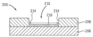
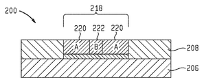
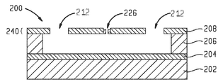
도 2a-2k는, 본원에 개시된 프로세스 흐름에 따른, 독립 멤브레인을 통해 형성된 하나 이상의 나노포어를 갖는 독립 멤브레인을 갖는 기판의 단면도들을 도시한다.
이해를 용이하게 하기 위해, 가능한 경우, 도면들에 공통된 동일한 요소들을 지시하는 데에 동일한 참조 번호들이 사용되었다. 일 양상의 요소들 및 특징들이 추가의 언급 없이 다른 양상들에 유익하게 통합될 수 있다는 것이 고려된다.
Claims (15)
- 기판을 형성하기 위한 방법으로서,
기판의 고도로 식각가능한 층 위에 박막을 갖는 기판을 제공하는 단계;
상기 고도로 식각가능한 층 위의 상기 박막을 통해 하나 이상의 나노포어를 형성하는 단계; 및
독립 멤브레인을 형성하기 위해, 상기 하나 이상의 나노포어 아래의 상기 고도로 식각가능한 층의 부분을 선택적으로 제거하는 단계를 포함하는, 기판을 형성하기 위한 방법. - 제1항에 있어서,
상기 고도로 식각가능한 층의 부분을 선택적으로 제거하는 단계는:
상기 기판을 식각 챔버에 위치시키는 것;
상기 고도로 식각가능한 층을 제거하기 위해 선택된 식각제를 상기 식각 챔버에 도입하는 것; 및
상기 고도로 식각가능한 층의 부분을 선택적으로 제거하기 위해 상기 기판을 상기 식각제에 노출시키는 것을 포함하는, 기판을 형성하기 위한 방법. - 제1항에 있어서,
상기 독립 멤브레인은 유전체 막이고, 상기 고도로 식각가능한 층은 규소를 포함하는, 기판을 형성하기 위한 방법. - 제1항에 있어서,
상기 독립 멤브레인의 적어도 일 측 상에 생물학적 샘플을 퇴적시키는 단계; 및
상기 생물학적 샘플을 상기 독립 멤브레인의 상기 하나 이상의 나노포어를 통해 지향시킴으로써 상기 생물학적 샘플을 분석하는 단계를 더 포함하는, 기판을 형성하기 위한 방법. - 제1항에 있어서,
상기 하나 이상의 나노포어의 각각의 직경은 약 100 나노미터 이하이고, 상기 독립 멤브레인의 두께는 약 50 나노미터 이하인, 기판을 형성하기 위한 방법. - 기판을 형성하기 위한 방법으로서,
기판의 고도로 식각가능한 층 위에 박막을 갖는 기판을 제공하는 단계;
포어 직경 감소 프로세스를 사용하여, 상기 고도로 식각가능한 층 위의 상기 박막을 통해 하나 이상의 나노포어를 형성하는 단계; 및
얇은 독립 멤브레인을 형성하기 위해, 상기 하나 이상의 나노포어 아래의 상기 고도로 식각가능한 층의 부분을 선택적으로 제거하는 단계를 포함하는, 기판을 형성하기 위한 방법. - 제6항에 있어서,
상기 고도로 식각가능한 층의 부분을 선택적으로 제거하는 단계는:
상기 기판을 상기 고도로 식각가능한 층의 부분을 선택적으로 제거하도록 선택된 식각제에 노출시키는 것을 포함하는, 기판을 형성하기 위한 방법. - 제6항에 있어서,
상기 독립 멤브레인의 적어도 일 측 상에 생물학적 샘플을 퇴적시키는 단계; 및
상기 생물학적 샘플을 상기 독립 멤브레인의 상기 하나 이상의 나노포어를 통해 지향시킴으로써 상기 생물학적 샘플을 분석하는 단계를 더 포함하는, 기판을 형성하기 위한 방법. - 제6항에 있어서,
상기 포어 직경 감소 프로세스는:
상기 박막에 적어도 하나의 제1 피쳐를 형성하는 단계;
상기 제1 피쳐에 블록 공중합체를 증착시키는 단계 ― 상기 블록 공중합체는 적어도 제1 도메인 및 제2 도메인을 포함함 ―; 및
상기 제2 도메인을 식각하는 단계를 포함하는, 기판을 형성하기 위한 방법. - 제6항에 있어서,
상기 포어 직경 감소 프로세스는:
상기 박막에 적어도 하나의 제1 피쳐를 형성하는 단계;
상기 적어도 하나의 제1 피쳐 위에 유전체 물질을 증착시키는 단계; 및
상기 적어도 하나의 제1 피쳐 위의 상기 유전체 물질의 부분을 식각하는 단계를 포함하는, 기판을 형성하기 위한 방법. - 제10항에 있어서,
상기 방법은:
적어도 하나의 나노포어가 형성될 때까지, 상기 유전체 물질을 증착시키는 단계 및 상기 유전체 물질의 부분을 식각하는 단계를 반복하는 것을 더 포함하는, 기판을 형성하기 위한 방법. - 제6항에 있어서,
상기 포어 직경 감소 프로세스는:
상기 박막에 적어도 하나의 제1 피쳐를 형성하는 단계;
적어도 하나의 개구부를 채우기 위해 상기 기판 위에 유전체 물질를 형성하기 위해서 상기 기판을 산화시키는 단계 ― 상기 유전체 물질은 상기 유전체 물질에 형성된 적어도 하나의 이음부를 가짐 ―; 및
적어도 하나의 나노포어를 형성하기 위해 상기 적어도 하나의 이음부를 활용하는 단계를 포함하는, 기판을 형성하기 위한 방법. - 제6항에 있어서,
상기 박막 위에 하나 이상의 추가적인 층을 증착시키는 단계; 및
상기 박막 위에 양의 전극 및 음의 전극을 증착시키는 단계를 더 포함하는, 기판을 형성하기 위한 방법. - 기판으로서,
제1 규소 층;
상기 제1 규소 층 위에 배치된 유전체 층;
상기 유전체 층의 부분 위에 배치된 제2 규소 층;
상기 제2 규소 층 위에 배치된 독립 멤브레인 ― 상기 독립 멤브레인은, 상기 독립 멤브레인을 통해 형성된, 적어도 하나의 나노포어 및 적어도 하나의 개구부를 가짐 ―;
상기 적어도 하나의 나노포어 아래에 배치된 제1 웰; 및
상기 적어도 하나의 나노포어 위에 배치된 제2 웰을 포함하는, 기판. - 제14항에 있어서,
상기 제1 웰 및 상기 제2 웰 중 적어도 하나에 DNA 함유 유체를 포함하고, 상기 적어도 하나의 나노포어의 각각의 직경은 약 100 나노미터 이하이고, 상기 독립 멤브레인의 두께는 약 50 나노미터 이하인, 기판.
Priority Applications (1)
| Application Number | Priority Date | Filing Date | Title |
|---|---|---|---|
| KR1020227021066A KR102587775B1 (ko) | 2017-09-22 | 2018-09-11 | 생물학적 응용들을 위한 독립 멤브레인을 생성하는 방법 |
Applications Claiming Priority (5)
| Application Number | Priority Date | Filing Date | Title |
|---|---|---|---|
| US201762561976P | 2017-09-22 | 2017-09-22 | |
| US62/561,976 | 2017-09-22 | ||
| US16/122,171 US10830756B2 (en) | 2017-09-22 | 2018-09-05 | Method to create a free-standing membrane for biological applications |
| US16/122,171 | 2018-09-05 | ||
| PCT/US2018/050383 WO2019060168A1 (en) | 2017-09-22 | 2018-09-11 | METHOD OF CREATING A SELF-SUPPORTING MEMBRANE FOR BIOLOGICAL APPLICATIONS |
Related Child Applications (1)
| Application Number | Title | Priority Date | Filing Date |
|---|---|---|---|
| KR1020227021066A Division KR102587775B1 (ko) | 2017-09-22 | 2018-09-11 | 생물학적 응용들을 위한 독립 멤브레인을 생성하는 방법 |
Publications (2)
| Publication Number | Publication Date |
|---|---|
| KR20200044992A true KR20200044992A (ko) | 2020-04-29 |
| KR102412947B1 KR102412947B1 (ko) | 2022-06-24 |
Family
ID=65808006
Family Applications (2)
| Application Number | Title | Priority Date | Filing Date |
|---|---|---|---|
| KR1020207011448A Active KR102412947B1 (ko) | 2017-09-22 | 2018-09-11 | 생물학적 응용들을 위한 독립 멤브레인을 생성하는 방법 |
| KR1020227021066A Active KR102587775B1 (ko) | 2017-09-22 | 2018-09-11 | 생물학적 응용들을 위한 독립 멤브레인을 생성하는 방법 |
Family Applications After (1)
| Application Number | Title | Priority Date | Filing Date |
|---|---|---|---|
| KR1020227021066A Active KR102587775B1 (ko) | 2017-09-22 | 2018-09-11 | 생물학적 응용들을 위한 독립 멤브레인을 생성하는 방법 |
Country Status (6)
| Country | Link |
|---|---|
| US (1) | US10830756B2 (ko) |
| EP (1) | EP3685434A4 (ko) |
| JP (1) | JP7101765B2 (ko) |
| KR (2) | KR102412947B1 (ko) |
| CN (1) | CN111108591B (ko) |
| WO (1) | WO2019060168A1 (ko) |
Families Citing this family (2)
| Publication number | Priority date | Publication date | Assignee | Title |
|---|---|---|---|---|
| KR102205435B1 (ko) | 2016-03-21 | 2021-01-21 | 온테라 인크. | 나노기공 감지를 위한 절연체-막-절연체 장치의 웨이퍼-척도 어셈블리 |
| US11486873B2 (en) | 2016-03-31 | 2022-11-01 | Ontera Inc. | Multipore determination of fractional abundance of polynucleotide sequences in a sample |
Citations (7)
| Publication number | Priority date | Publication date | Assignee | Title |
|---|---|---|---|---|
| WO2009045473A2 (en) * | 2007-10-02 | 2009-04-09 | President And Fellows Of Harvard College | Carbon nanotube synthesis for nanopore devices |
| KR20100126190A (ko) * | 2009-05-22 | 2010-12-01 | 인터내셔널 비지네스 머신즈 코포레이션 | 중합체의 유도된 자기조립을 이용하여 서브리쏘그래픽 피처를 형성하는 방법 |
| US20120021204A1 (en) * | 2010-07-26 | 2012-01-26 | International Business Machines Corporation | Structure and method to form nanopore |
| US20120108068A1 (en) * | 2010-11-03 | 2012-05-03 | Texas Instruments Incorporated | Method for Patterning Sublithographic Features |
| US20150284791A1 (en) * | 2014-04-08 | 2015-10-08 | International Business Machines Corporation | Reduction of entropic barrier of polyelectrolyte molecules in a nanopore device with agarose gel |
| US20160042971A1 (en) * | 2014-08-07 | 2016-02-11 | Tokyo Electron Limited | Method for Directed Self-Assembly and Pattern Curing |
| WO2016056887A1 (en) * | 2014-10-09 | 2016-04-14 | Mimos Berhad | Humidity sensor with nanoporous polyimide membranes and a method of fabrication thereof |
Family Cites Families (10)
| Publication number | Priority date | Publication date | Assignee | Title |
|---|---|---|---|---|
| US8512588B2 (en) | 2010-08-13 | 2013-08-20 | Lawrence Livermore National Security, Llc | Method of fabricating a scalable nanoporous membrane filter |
| EP2562135A1 (de) | 2011-08-22 | 2013-02-27 | ETH Zurich | Verfahren zur Herstellung und Ausrichtung von Nanowires und Anwendungen eines solchen Verfahrens |
| MX357200B (es) | 2012-05-07 | 2018-06-29 | Univ Ottawa | Fabricacion de nanoporos utilizando campos electricos elevados. |
| WO2013188841A1 (en) * | 2012-06-15 | 2013-12-19 | Genia Technologies, Inc. | Chip set-up and high-accuracy nucleic acid sequencing |
| CA3116407C (en) | 2013-03-15 | 2023-02-07 | President And Fellows Of Harvard College | Surface wetting method |
| US9046511B2 (en) * | 2013-04-18 | 2015-06-02 | International Business Machines Corporation | Fabrication of tunneling junction for nanopore DNA sequencing |
| US9230820B2 (en) | 2013-10-30 | 2016-01-05 | HGST Netherlands B.V. | Method for directed self-assembly (DSA) of a block copolymer (BCP) using a blend of a BCP with functional homopolymers |
| FR3023581B1 (fr) | 2014-07-08 | 2016-07-15 | Snecma | Montage d'aubes en peripherie d'un disque de turbomachine |
| MX388279B (es) | 2014-12-19 | 2025-03-18 | Univ Ottawa | Integracion de sensores de nanoporos dentro de agrupaciones de canales microfluidicos usando descargas disruptivas controladas. |
| US9945836B2 (en) * | 2015-04-23 | 2018-04-17 | International Business Machines Corporation | Field effect based nanopore device |
-
2018
- 2018-09-05 US US16/122,171 patent/US10830756B2/en active Active
- 2018-09-11 KR KR1020207011448A patent/KR102412947B1/ko active Active
- 2018-09-11 CN CN201880060589.0A patent/CN111108591B/zh not_active Expired - Fee Related
- 2018-09-11 JP JP2020516550A patent/JP7101765B2/ja active Active
- 2018-09-11 WO PCT/US2018/050383 patent/WO2019060168A1/en not_active Ceased
- 2018-09-11 EP EP18859772.8A patent/EP3685434A4/en not_active Withdrawn
- 2018-09-11 KR KR1020227021066A patent/KR102587775B1/ko active Active
Patent Citations (7)
| Publication number | Priority date | Publication date | Assignee | Title |
|---|---|---|---|---|
| WO2009045473A2 (en) * | 2007-10-02 | 2009-04-09 | President And Fellows Of Harvard College | Carbon nanotube synthesis for nanopore devices |
| KR20100126190A (ko) * | 2009-05-22 | 2010-12-01 | 인터내셔널 비지네스 머신즈 코포레이션 | 중합체의 유도된 자기조립을 이용하여 서브리쏘그래픽 피처를 형성하는 방법 |
| US20120021204A1 (en) * | 2010-07-26 | 2012-01-26 | International Business Machines Corporation | Structure and method to form nanopore |
| US20120108068A1 (en) * | 2010-11-03 | 2012-05-03 | Texas Instruments Incorporated | Method for Patterning Sublithographic Features |
| US20150284791A1 (en) * | 2014-04-08 | 2015-10-08 | International Business Machines Corporation | Reduction of entropic barrier of polyelectrolyte molecules in a nanopore device with agarose gel |
| US20160042971A1 (en) * | 2014-08-07 | 2016-02-11 | Tokyo Electron Limited | Method for Directed Self-Assembly and Pattern Curing |
| WO2016056887A1 (en) * | 2014-10-09 | 2016-04-14 | Mimos Berhad | Humidity sensor with nanoporous polyimide membranes and a method of fabrication thereof |
Non-Patent Citations (2)
| Title |
|---|
| Axel Fanget 등, "Nanopore Integrated Nanogaps for DNA Detection", Nano Letters, 2013.12.06., Vol. 14, No. 1, 페이지 244-249* * |
| Miao Zhang 등, "Oxidation of nanopores in a silicon membrane: self-limiting formation of sub-10nm circular openings", Nanotechnology, 2014.08.12., Vol. 25, No. 35.* * |
Also Published As
| Publication number | Publication date |
|---|---|
| KR20220095250A (ko) | 2022-07-06 |
| KR102587775B1 (ko) | 2023-10-12 |
| US10830756B2 (en) | 2020-11-10 |
| CN111108591B (zh) | 2021-06-08 |
| JP7101765B2 (ja) | 2022-07-15 |
| WO2019060168A1 (en) | 2019-03-28 |
| JP2020534009A (ja) | 2020-11-26 |
| EP3685434A1 (en) | 2020-07-29 |
| US20190094203A1 (en) | 2019-03-28 |
| KR102412947B1 (ko) | 2022-06-24 |
| CN111108591A (zh) | 2020-05-05 |
| EP3685434A4 (en) | 2021-06-16 |
Similar Documents
| Publication | Publication Date | Title |
|---|---|---|
| US10994991B2 (en) | Method to reduce pore diameter using atomic layer deposition and etching | |
| US11691872B2 (en) | Pore formation in a substrate | |
| US20120256281A1 (en) | Semiconductor devices having nanochannels confined by nanometer-spaced electrodes | |
| KR102587775B1 (ko) | 생물학적 응용들을 위한 독립 멤브레인을 생성하는 방법 | |
| KR20200046120A (ko) | 나노포어의 간단한 유체공학적 처리를 위한 방법 | |
| KR102544057B1 (ko) | 나노포어를 형성하는 방법 및 결과적인 구조 | |
| KR20220004792A (ko) | 이중 포어 센서들 | |
| KR20220004793A (ko) | 이중 포어 센서들을 위한 제조 방법들 |
Legal Events
| Date | Code | Title | Description |
|---|---|---|---|
| A201 | Request for examination | ||
| PA0105 | International application |
St.27 status event code: A-0-1-A10-A15-nap-PA0105 |
|
| PA0201 | Request for examination |
St.27 status event code: A-1-2-D10-D11-exm-PA0201 |
|
| PG1501 | Laying open of application |
St.27 status event code: A-1-1-Q10-Q12-nap-PG1501 |
|
| E902 | Notification of reason for refusal | ||
| PE0902 | Notice of grounds for rejection |
St.27 status event code: A-1-2-D10-D21-exm-PE0902 |
|
| AMND | Amendment | ||
| P11-X000 | Amendment of application requested |
St.27 status event code: A-2-2-P10-P11-nap-X000 |
|
| P13-X000 | Application amended |
St.27 status event code: A-2-2-P10-P13-nap-X000 |
|
| E601 | Decision to refuse application | ||
| PE0601 | Decision on rejection of patent |
St.27 status event code: N-2-6-B10-B15-exm-PE0601 |
|
| X091 | Application refused [patent] | ||
| AMND | Amendment | ||
| E13-X000 | Pre-grant limitation requested |
St.27 status event code: A-2-3-E10-E13-lim-X000 |
|
| P11-X000 | Amendment of application requested |
St.27 status event code: A-2-2-P10-P11-nap-X000 |
|
| P13-X000 | Application amended |
St.27 status event code: A-2-2-P10-P13-nap-X000 |
|
| PX0901 | Re-examination |
St.27 status event code: A-2-3-E10-E12-rex-PX0901 |
|
| PX0701 | Decision of registration after re-examination |
St.27 status event code: A-3-4-F10-F13-rex-PX0701 |
|
| X701 | Decision to grant (after re-examination) | ||
| A107 | Divisional application of patent | ||
| GRNT | Written decision to grant | ||
| PA0104 | Divisional application for international application |
St.27 status event code: A-0-1-A10-A18-div-PA0104 St.27 status event code: A-0-1-A10-A16-div-PA0104 |
|
| PR0701 | Registration of establishment |
St.27 status event code: A-2-4-F10-F11-exm-PR0701 |
|
| PR1002 | Payment of registration fee |
St.27 status event code: A-2-2-U10-U12-oth-PR1002 Fee payment year number: 1 |
|
| PG1601 | Publication of registration |
St.27 status event code: A-4-4-Q10-Q13-nap-PG1601 |
|
| PR1001 | Payment of annual fee |
St.27 status event code: A-4-4-U10-U11-oth-PR1001 Fee payment year number: 4 |
|
| U11 | Full renewal or maintenance fee paid |
Free format text: ST27 STATUS EVENT CODE: A-4-4-U10-U11-OTH-PR1001 (AS PROVIDED BY THE NATIONAL OFFICE) Year of fee payment: 4 |
|
| P22-X000 | Classification modified |
St.27 status event code: A-4-4-P10-P22-nap-X000 |
|
| P22-X000 | Classification modified |
St.27 status event code: A-4-4-P10-P22-nap-X000 |