KR20200045573A - 다층 오버레이 계측 타겟 및 상보적 오버레이 계측 측정 시스템 - Google Patents
다층 오버레이 계측 타겟 및 상보적 오버레이 계측 측정 시스템 Download PDFInfo
- Publication number
- KR20200045573A KR20200045573A KR1020207011567A KR20207011567A KR20200045573A KR 20200045573 A KR20200045573 A KR 20200045573A KR 1020207011567 A KR1020207011567 A KR 1020207011567A KR 20207011567 A KR20207011567 A KR 20207011567A KR 20200045573 A KR20200045573 A KR 20200045573A
- Authority
- KR
- South Korea
- Prior art keywords
- target
- target structure
- overlay
- structures
- symmetry
- Prior art date
- Legal status (The legal status is an assumption and is not a legal conclusion. Google has not performed a legal analysis and makes no representation as to the accuracy of the status listed.)
- Granted
Links
Images


Classifications
-
- H—ELECTRICITY
- H10—SEMICONDUCTOR DEVICES; ELECTRIC SOLID-STATE DEVICES NOT OTHERWISE PROVIDED FOR
- H10W—GENERIC PACKAGES, INTERCONNECTIONS, CONNECTORS OR OTHER CONSTRUCTIONAL DETAILS OF DEVICES COVERED BY CLASS H10
- H10W46/00—Marks applied to devices, e.g. for alignment or identification
-
- H01L21/0273—
-
- G—PHYSICS
- G03—PHOTOGRAPHY; CINEMATOGRAPHY; ANALOGOUS TECHNIQUES USING WAVES OTHER THAN OPTICAL WAVES; ELECTROGRAPHY; HOLOGRAPHY
- G03F—PHOTOMECHANICAL PRODUCTION OF TEXTURED OR PATTERNED SURFACES, e.g. FOR PRINTING, FOR PROCESSING OF SEMICONDUCTOR DEVICES; MATERIALS THEREFOR; ORIGINALS THEREFOR; APPARATUS SPECIALLY ADAPTED THEREFOR
- G03F7/00—Photomechanical, e.g. photolithographic, production of textured or patterned surfaces, e.g. printing surfaces; Materials therefor, e.g. comprising photoresists; Apparatus specially adapted therefor
- G03F7/70—Microphotolithographic exposure; Apparatus therefor
- G03F7/70483—Information management; Active and passive control; Testing; Wafer monitoring, e.g. pattern monitoring
- G03F7/70605—Workpiece metrology
- G03F7/70616—Monitoring the printed patterns
- G03F7/70633—Overlay, i.e. relative alignment between patterns printed by separate exposures in different layers, or in the same layer in multiple exposures or stitching
-
- G—PHYSICS
- G03—PHOTOGRAPHY; CINEMATOGRAPHY; ANALOGOUS TECHNIQUES USING WAVES OTHER THAN OPTICAL WAVES; ELECTROGRAPHY; HOLOGRAPHY
- G03F—PHOTOMECHANICAL PRODUCTION OF TEXTURED OR PATTERNED SURFACES, e.g. FOR PRINTING, FOR PROCESSING OF SEMICONDUCTOR DEVICES; MATERIALS THEREFOR; ORIGINALS THEREFOR; APPARATUS SPECIALLY ADAPTED THEREFOR
- G03F7/00—Photomechanical, e.g. photolithographic, production of textured or patterned surfaces, e.g. printing surfaces; Materials therefor, e.g. comprising photoresists; Apparatus specially adapted therefor
- G03F7/70—Microphotolithographic exposure; Apparatus therefor
- G03F7/70483—Information management; Active and passive control; Testing; Wafer monitoring, e.g. pattern monitoring
- G03F7/70605—Workpiece metrology
- G03F7/70616—Monitoring the printed patterns
-
- G—PHYSICS
- G03—PHOTOGRAPHY; CINEMATOGRAPHY; ANALOGOUS TECHNIQUES USING WAVES OTHER THAN OPTICAL WAVES; ELECTROGRAPHY; HOLOGRAPHY
- G03F—PHOTOMECHANICAL PRODUCTION OF TEXTURED OR PATTERNED SURFACES, e.g. FOR PRINTING, FOR PROCESSING OF SEMICONDUCTOR DEVICES; MATERIALS THEREFOR; ORIGINALS THEREFOR; APPARATUS SPECIALLY ADAPTED THEREFOR
- G03F7/00—Photomechanical, e.g. photolithographic, production of textured or patterned surfaces, e.g. printing surfaces; Materials therefor, e.g. comprising photoresists; Apparatus specially adapted therefor
- G03F7/70—Microphotolithographic exposure; Apparatus therefor
- G03F7/70483—Information management; Active and passive control; Testing; Wafer monitoring, e.g. pattern monitoring
- G03F7/70605—Workpiece metrology
- G03F7/70681—Metrology strategies
- G03F7/70683—Mark designs
-
- G—PHYSICS
- G03—PHOTOGRAPHY; CINEMATOGRAPHY; ANALOGOUS TECHNIQUES USING WAVES OTHER THAN OPTICAL WAVES; ELECTROGRAPHY; HOLOGRAPHY
- G03F—PHOTOMECHANICAL PRODUCTION OF TEXTURED OR PATTERNED SURFACES, e.g. FOR PRINTING, FOR PROCESSING OF SEMICONDUCTOR DEVICES; MATERIALS THEREFOR; ORIGINALS THEREFOR; APPARATUS SPECIALLY ADAPTED THEREFOR
- G03F7/00—Photomechanical, e.g. photolithographic, production of textured or patterned surfaces, e.g. printing surfaces; Materials therefor, e.g. comprising photoresists; Apparatus specially adapted therefor
- G03F7/70—Microphotolithographic exposure; Apparatus therefor
- G03F7/70483—Information management; Active and passive control; Testing; Wafer monitoring, e.g. pattern monitoring
- G03F7/70605—Workpiece metrology
- G03F7/706843—Metrology apparatus
- G03F7/706845—Calibration, e.g. tool-to-tool calibration, beam alignment, spot position or focus
-
- G—PHYSICS
- G03—PHOTOGRAPHY; CINEMATOGRAPHY; ANALOGOUS TECHNIQUES USING WAVES OTHER THAN OPTICAL WAVES; ELECTROGRAPHY; HOLOGRAPHY
- G03F—PHOTOMECHANICAL PRODUCTION OF TEXTURED OR PATTERNED SURFACES, e.g. FOR PRINTING, FOR PROCESSING OF SEMICONDUCTOR DEVICES; MATERIALS THEREFOR; ORIGINALS THEREFOR; APPARATUS SPECIALLY ADAPTED THEREFOR
- G03F9/00—Registration or positioning of originals, masks, frames, photographic sheets or textured or patterned surfaces, e.g. automatically
- G03F9/70—Registration or positioning of originals, masks, frames, photographic sheets or textured or patterned surfaces, e.g. automatically for microlithography
- G03F9/7073—Alignment marks and their environment
- G03F9/7076—Mark details, e.g. phase grating mark, temporary mark
-
- G—PHYSICS
- G03—PHOTOGRAPHY; CINEMATOGRAPHY; ANALOGOUS TECHNIQUES USING WAVES OTHER THAN OPTICAL WAVES; ELECTROGRAPHY; HOLOGRAPHY
- G03F—PHOTOMECHANICAL PRODUCTION OF TEXTURED OR PATTERNED SURFACES, e.g. FOR PRINTING, FOR PROCESSING OF SEMICONDUCTOR DEVICES; MATERIALS THEREFOR; ORIGINALS THEREFOR; APPARATUS SPECIALLY ADAPTED THEREFOR
- G03F9/00—Registration or positioning of originals, masks, frames, photographic sheets or textured or patterned surfaces, e.g. automatically
- G03F9/70—Registration or positioning of originals, masks, frames, photographic sheets or textured or patterned surfaces, e.g. automatically for microlithography
- G03F9/7088—Alignment mark detection, e.g. TTR, TTL, off-axis detection, array detector, video detection
-
- H—ELECTRICITY
- H10—SEMICONDUCTOR DEVICES; ELECTRIC SOLID-STATE DEVICES NOT OTHERWISE PROVIDED FOR
- H10P—GENERIC PROCESSES OR APPARATUS FOR THE MANUFACTURE OR TREATMENT OF DEVICES COVERED BY CLASS H10
- H10P72/00—Handling or holding of wafers, substrates or devices during manufacture or treatment thereof
- H10P72/50—Handling or holding of wafers, substrates or devices during manufacture or treatment thereof for positioning, orientation or alignment
- H10P72/53—Handling or holding of wafers, substrates or devices during manufacture or treatment thereof for positioning, orientation or alignment using optical controlling means
-
- H—ELECTRICITY
- H10—SEMICONDUCTOR DEVICES; ELECTRIC SOLID-STATE DEVICES NOT OTHERWISE PROVIDED FOR
- H10P—GENERIC PROCESSES OR APPARATUS FOR THE MANUFACTURE OR TREATMENT OF DEVICES COVERED BY CLASS H10
- H10P76/00—Manufacture or treatment of masks on semiconductor bodies, e.g. by lithography or photolithography
- H10P76/20—Manufacture or treatment of masks on semiconductor bodies, e.g. by lithography or photolithography of masks comprising organic materials
- H10P76/204—Manufacture or treatment of masks on semiconductor bodies, e.g. by lithography or photolithography of masks comprising organic materials of organic photoresist masks
-
- H—ELECTRICITY
- H10—SEMICONDUCTOR DEVICES; ELECTRIC SOLID-STATE DEVICES NOT OTHERWISE PROVIDED FOR
- H10W—GENERIC PACKAGES, INTERCONNECTIONS, CONNECTORS OR OTHER CONSTRUCTIONAL DETAILS OF DEVICES COVERED BY CLASS H10
- H10W46/00—Marks applied to devices, e.g. for alignment or identification
- H10W46/301—Marks applied to devices, e.g. for alignment or identification for alignment
Landscapes
- Physics & Mathematics (AREA)
- General Physics & Mathematics (AREA)
- Engineering & Computer Science (AREA)
- Multimedia (AREA)
- Exposure And Positioning Against Photoresist Photosensitive Materials (AREA)
- Length Measuring Devices By Optical Means (AREA)
- Exposure Of Semiconductors, Excluding Electron Or Ion Beam Exposure (AREA)
Abstract
Description
도 1a는 오버레이 타겟의 상면도이다.
도 1b는 오버레이 타겟의 상면도이다.
도 2a는 오버레이 타겟의 상면도이다.
도 2b는 오버레이 타겟의 상면도이다.
도 3은 본 발명의 일 실시형태에 따른 다층 오버레이 타겟의 상면도이다.
도 4는 본 발명의 일 실시형태에 따른 다층 오버레이 타겟의 상면도이다.
도 5a는 본 발명의 일 실시형태에 따른 다층 오버레이 타겟의 상면도이다.
도 5b는 본 발명의 일 실시형태에 따른 다층 오버레이 타겟의 상면도이다.
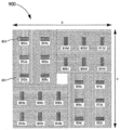
도 6은 본 발명의 일 실시형태에 따른 다층 오버레이 타겟의 상면도이다.
도 7은 본 발명의 일 실시형태에 따른 다층 오버레이 타겟의 상면도이다.
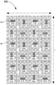
도 8은 본 발명의 일 실시형태에 따른 더미 필의 존재하에 인쇄된 다층 오버레이 타겟의 상면도이다.
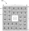
도 9는 본 발명의 일 실시형태에 따른 더미 필의 존재하에 인쇄된 다층 오버레이 타겟의 상면도이다.
도 10은 본 발명의 일 실시형태에 따른 더미 필의 존재하에 인쇄된 다층 오버레이 타겟의 상면도이다.
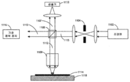
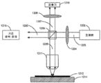
도 11은 다층 오버레이 계측 타겟의 콘트라스트 향상에 적합한 시스템의 블록도이다.
도 12는 다층 오버레이 계측 타겟의 콘트라스트 향상에 적합한 시스템의 블록도이다.
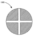
도 13a는 본 발명의 일 실시형태에 따른 콘트라스트 향상에 적합한 조명 동공 구조의 개략도이다.
도 13b는 본 발명의 일 실시형태에 따른 콘트라스트 향상에 적합한 조명 동공 구조의 개략도이다.
도 13c는 본 발명의 일 실시형태에 따른 콘트라스트 향상에 적합한 조명 동공 구조의 개략도이다.
Claims (48)
- 다층 오버레이 타겟에 있어서,
3개 이상의 타겟 구조물들을 포함하는 복수의 타겟 구조물들을 포함하고,
상기 3개 이상의 타겟 구조물들은 제1 타겟 구조물, 제2 타겟 구조물 및 적어도 제3 타겟 구조물을 포함하고, 상기 타겟 구조물들 중 적어도 몇몇의 타겟 구조물들은 2개 이상의 패턴 요소(pattern element)들의 집합을 포함하고,
상기 3개 이상의 타겟 구조물들은 상기 3개 이상의 타겟 구조물들의 정렬시에 공통 대칭 중심을 공유하도록 구성되며, 상기 타겟 구조물들 중 적어도 하나의 타겟 구조물은 상기 공통 대칭 중심에 대한 90도 회전에 대해 불변체(invariant)이고,
상기 제1 타겟 구조물은 제1 공정 층에 배치되고, 상기 제2 타겟 구조물은 상기 제1 공정 층과는 상이한 제2 공정 층에 배치되고, 적어도 상기 제3 타겟 구조물은 적어도 제3 공정 층에 배치되며, 상기 적어도 제3 공정 층은 상기 제1 공정 층 및 상기 제2 공정 층과는 상이하고,
상기 2개 이상의 패턴 요소들의 집합의 제1 특정 패턴 요소는 3개 이상의 하위 요소(sub-element)들을 포함하고, 상기 2개 이상의 패턴 요소들의 집합의 적어도 제2 특정 패턴 요소는 3개 이상의 하위 요소(sub-element)들을 포함하고,
상기 제1 특정 패턴 요소의 3개 이상의 하위 요소들 및 상기 적어도 제2 특정 패턴 요소의 3개 이상의 하위 요소들 중, 적어도 하나는, 선택된 방향을 따라 정렬되며 상기 선택된 방향에 수직한 방향을 따라 분산되는 3개 이상의 평행선 구조들의 집합을 포함하는 것인, 다층 오버레이 타겟. - 제1항에 있어서,
상기 2개 이상의 패턴 요소들의 집합의 제1 패턴 요소는 제1 방향에서의 오버레이 계측 측정에 적합하고, 상기 2개 이상의 패턴 요소들의 집합의 제2 패턴 요소는 상기 제1 방향과 상이한 제2 방향에서의 오버레이 계측 측정에 적합한 것인, 다층 오버레이 타겟. - 제1항에 있어서,
제1 방향에서의 오버레이 계측 측정에 적합한 패턴 요소들의 집합 및 상기 제1 방향과 상이한 방향에서의 오버레이 계측 측정에 적합한 패턴 요소들의 제2 집합은 공통 대칭 중심을 갖는 것인, 다층 오버레이 타겟. - 제1항에 있어서,
각 타겟 구조물의 상기 2개 이상의 패턴 요소들의 집합은 더미 필의 층 위 또는 아래에 인쇄되는 것인, 다층 오버레이 타겟. - 제1항에 있어서,
상기 복수의 타겟 구조물 중 몇몇의 타겟 구조물들은, 상기 복수의 타겟 구조물의 상기 몇몇의 타겟 구조물들의 콘트라스트를 향상시키기 위한 추가의 패턴 요소들의 집합을 포함하는 것인, 다층 오버레이 타겟.
레이 측정 시스템. - 제1항에 있어서,
각각의 타겟 구조물의 상기 2개 이상의 패턴 요소들 중 적어도 몇몇의 패턴 요소들은, 개별적인 대칭 중심에 대한 180도 회전에 대해 불변체이며 상기 개별적인 대칭 중심에 대한 90도 회전에 대해 가변체인 것인, 다층 오버레이 타겟. - 제1항에 있어서,
상기 제1 타겟 구조물은 상기 공통 대칭 중심에 대한 90도 회전에 대해 불변체이고,
상기 제2 타겟 구조물 및 적어도 상기 제3 타겟 구조물은, 상기 공통 대칭 중심에 대한 180도 회전에 대해 불변체이며 상기 공통 대칭 중심에 대한 90도 회전에 대해서는 가변체인 것인, 다층 오버레이 타겟. - 제1항에 있어서,
상기 제1 타겟 구조물은 제1 방향 및 상기 제1 방향에 대해 수직한 제2 방향에서 오버레이를 측정하도록 구성되며,
상기 제2 타겟 구조물은 상기 제1 방향으로 오버레이를 측정하도록 구성되며,
상기 제3 타겟 구조물은 상기 제2 방향으로 오버레이를 측정하도록 구성된 것인, 다층 오버레이 타겟. - 제1항에 있어서,
상기 제1 타겟 구조물은 공통 대칭 중심에 대한 90도 회전에 대해 불변체이고,
상기 제2 타겟 구조물 및 상기 제3 타겟 구조물 중 적어도 하나는, 상기 공통 대칭 중심에 대한 180도 회전에 대해서 불변체이며 상기 공통 대칭 중심에 대한 90도 회전에 대해서는 가변체이고,
각각의 타겟 구조물의 상기 2개 이상의 패턴 요소들 각각은, 개별적인 대칭 중심에 대한 180도 회전에 대해 불변체이며 상기 개별적인 대칭 중심에 대한 90도 회전에 대해서는 가변체인 것인, 다층 오버레이 타겟. - 제1항에 있어서,
상기 3개 이상의 하위 요소들은 상기 패턴 요소들 중 적어도 하나의 패턴 요소의 간격에 대해 평행하게 배열된 것인, 다층 오버레이 타겟. - 제1항에 있어서,
상기 3개 이상의 하위 요소들은 상기 패턴 요소들 중 적어도 하나의 패턴 요소의 간격에 대해 수직하게 배열된 것인, 다층 오버레이 타겟. - 제1항에 있어서,
상기 3개 이상의 하위 요소들은, 상기 패턴 요소들 중 적어도 하나의 패턴 요소의 제1 간격에 대해 평행하게 배열되며 상기 패턴 요소들 중 적어도 하나의 패턴 요소의 제2 간격에 대해 수직하게 배열된 것인, 다층 오버레이 타겟. - 제1항에 있어서,
상기 3개 이상의 하위 요소들과 관련된 간격은 상기 패턴 요소들 중 2개 이상의 패턴 요소들 간의 간격보다 작은 것인, 다층 오버레이 타겟. - 제1항에 있어서,
상기 2개 이상의 패턴 요소들 중 적어도 몇몇의 패턴 요소들은 개별적인 대칭 중심을 갖는 것인, 다층 오버레이 타겟. - 다층 오버레이 타겟에 있어서,
3개 이상의 타겟 구조물들을 포함하는 복수의 타겟 구조물들을 포함하고,
상기 3개 이상의 타겟 구조물들은 제1 타겟 구조물, 제2 타겟 구조물 및 적어도 제3 타겟 구조물을 포함하고, 상기 타겟 구조물들 중 적어도 몇몇의 타겟 구조물들은 2개 이상의 패턴 요소(pattern element)들의 집합을 포함하고,
상기 3개 이상의 타겟 구조물들은 상기 3개 이상의 타겟 구조물들의 정렬시에 공통 대칭 중심을 공유하도록 구성되며, 상기 제1 타겟 구조물은 상기 공통 대칭 중심에 대한 90도 회전에 대해 불변체(invariant)이고, 상기 제2 타겟 구조물은 상기 공통 대칭 중심에 대한 90도 회전에 대해 불변체이고, 적어도 상기 제3 타겟 구조물은 상기 공통 대칭 중심에 대한 90도 회전에 대해 불변체이며,
상기 제1 타겟 구조물은 제1 공정 층에 배치되고, 상기 제2 타겟 구조물은 상기 제1 공정 층과는 상이한 제2 공정 층에 배치되고, 적어도 상기 제3 타겟 구조물은 적어도 제3 공정 층에 배치되며, 상기 적어도 제3 공정 층은 상기 제1 공정 층 및 상기 제2 공정 층과는 상이하고,
상기 2개 이상의 패턴 요소들 중 적어도 몇몇의 패턴 요소들은 상기 3개 이상의 타겟 구조물들의 상기 공통 대칭 중심과 상이한 개별적인 대칭 중심을 가지고,
상기 제1 타겟 구조물의 패턴 요소의 적어도 일부는 상기 제2 타겟 구조물 및 상기 적어도 제3 타겟 구조물 중 적어도 하나의 타겟 구조물의 패턴 요소의 적어도 일부와 중첩하는 것인, 다층 오버레이 타겟. - 제15항에 있어서,
상기 3개 이상의 타겟 구조물은 적어도 제4 타겟 구조물을 포함하는 것인, 다층 오버레이 타겟. - 제16항에 있어서,
적어도 상기 제4 타겟 구조물은 상기 공통 대칭 중심에 대한 90도 회전에 대해 불변체인 것인, 다층 오버레이 타겟. - 제17항에 있어서,
상기 제1 타겟 구조물, 상기 제2 타겟 구조물, 상기 제3 타겟 구조물 및 상기 제4 타겟 구조물은 제1 방향 및 상기 제1 방향에 수직한 제2 방향으로 오버레이를 측정하도록 구성된 것인, 다층 오버레이 타겟. - 제15항에 있어서,
상기 제1 타겟 구조물의 하나 이상의 패턴 요소는 상기 제2 타겟 구조물 및 상기 적어도 제3 타겟 구조물 중 적어도 하나의 타겟 구조물의 하나 이상의 패턴 요소와 중첩하는 것인, 다층 오버레이 타겟. - 다층 오버레이 타겟에 있어서,
3개 이상의 타겟 구조물들을 포함하는 복수의 타겟 구조물들을 포함하고,
상기 3개 이상의 타겟 구조물들은 제1 타겟 구조물, 제2 타겟 구조물 및 적어도 제3 타겟 구조물을 포함하고, 상기 타겟 구조물들 중 적어도 몇몇의 타겟 구조물들은 2개 이상의 패턴 요소(pattern element)들의 집합을 포함하고, 상기 2개 이상의 패턴 요소들 중 적어도 몇몇의 패턴 요소들은 반사 불변체(reflection invariant)이고,
각각의 타겟 구조물의 상기 2개 이상의 패턴 요소들의 적어도 몇몇의 패턴 요소들은 개별적인 대칭 중심에 대한 90도 회전에 대해 가변체이고,
상기 다층 오버레이 타겟의 상기 2개 이상의 패턴 요소들은 서로 공간적으로 분리되어 있으며,
상기 3개 이상의 타겟 구조물들은 상기 3개 이상의 타겟 구조물들의 정렬시에 공통 대칭 중심을 공유하도록 구성되고,
상기 제1 타겟 구조물은 제1 공정 층에 배치되고, 상기 제2 타겟 구조물은 상기 제1 공정 층과는 상이한 제2 공정 층에 배치되고, 적어도 상기 제3 타겟 구조물은 적어도 제3 공정 층에 배치되며, 상기 적어도 제3 공정 층은 상기 제1 공정 층 및 상기 제2 공정 층과는 상이한 것인, 다층 오버레이 타겟. - 다층 오버레이 타겟에 있어서,
3개 이상의 타겟 구조물들을 포함하는 복수의 타겟 구조물들을 포함하고,
상기 3개 이상의 타겟 구조물들은 제1 타겟 구조물, 제2 타겟 구조물 및 적어도 제3 타겟 구조물을 포함하고, 상기 타겟 구조물들 중 적어도 몇몇의 타겟 구조물들은 2개 이상의 패턴 요소(pattern element)들의 집합을 포함하고,
상기 다층 오버레이 타겟의 상기 2개 이상의 패턴 요소들은 서로 공간적으로 분리되어 있으며,
상기 타겟 구조물들 중 적어도 몇몇의 타겟 구조물들은 반사 불변체(reflection invariant)이고,
각각의 타겟 구조물의 상기 2개 이상의 패턴 요소들 중 적어도 몇몇의 패턴 요소들은 반사 불변체이며 개별적인 대칭 중심에 대한 90도 회전에 대해 가변체이고,
상기 3개 이상의 타겟 구조물들은 상기 3개 이상의 타겟 구조물들의 정렬시에 공통 대칭 중심을 공유하도록 구성되고,
상기 제1 타겟 구조물은 제1 공정 층에 배치되고, 상기 제2 타겟 구조물은 상기 제1 공정 층과는 상이한 제2 공정 층에 배치되고, 적어도 상기 제3 타겟 구조물은 적어도 제3 공정 층에 배치되며, 상기 적어도 제3 공정 층은 상기 제1 공정 층 및 상기 제2 공정 층과는 상이한 것인, 다층 오버레이 타겟. - 다층 오버레이 타겟에 있어서,
4개 이상의 타겟 구조물들을 포함하는 복수의 타겟 구조물들을 포함하고,
상기 4개 이상의 타겟 구조물들은 제1 타겟 구조물, 제2 타겟 구조물, 제3 타겟 구조물 및 적어도 제4 타겟 구조물을 포함하고, 상기 타겟 구조물들 중 적어도 몇몇의 타겟 구조물들은 2개 이상의 패턴 요소(pattern element)들의 집합을 포함하고,
상기 다층 오버레이 타겟의 상기 2개 이상의 패턴 요소들은 서로 공간적으로 분리되어 있으며,
상기 2개 이상의 패턴 요소들 중 적어도 하나의 패턴 요소는 개별적인 대칭 중심에 대한 90도 회전에 대해 가변체이고,
상기 4개 이상의 타겟 구조물 각각의 대칭 중심의 위치는 상기 4개 이상의 타겟 구조물들의 오버레이 정렬을 나타내고,
상기 4개 이상의 타겟 구조물들은 상기 4개 이상의 타겟 구조물들의 정렬시에 공통 대칭 중심을 공유하도록 구성되고,
상기 제1 타겟 구조물, 상기 제2 타겟 구조물, 상기 제3 타겟 구조물 및 상기 제4 타겟 구조물은 상기 공통 대칭 중심에 대한 180도 회전에 대해 불변체이며 상기 공통 대칭 중심에 대한 90도 회전에 대해서는 가변체이고,
상기 제1 타겟 구조물은 제1 공정 층에 배치되고, 상기 제2 타겟 구조물은 상기 제1 공정 층과는 상이한 제2 공정 층에 배치되고, 상기 제3 타겟 구조물은 상기 제1 공정 층 및 상기 제2 공정 층과는 상이한 제3 공정 층에 배치되며, 상기 적어도 제4 타겟 구조물은 상기 제1 공정 층, 상기 제2 공정 층 및 상기 제3 공정 층과는 상이한 제4 공정 층에 배치된 것인, 다층 오버레이 타겟. - 제22항에 있어서,
상기 제1 타겟 구조물 및 상기 제2 타겟 구조물 중 적어도 하나의 타겟 구조물은 제1 방향으로 오버레이를 측정하도록 구성되며,
상기 제3 타겟 구조물 및 상기 제4 타겟 구조물 중 적어도 하나의 타겟 구조물은 상기 제1 방향에 수직한 제2 방향으로 오버레이를 측정하도록 구성되는 것인, 다층 오버레이 타겟. - 제22항에 있어서,
각각의 타겟 구조물의 상기 2개 이상의 패턴 요소들 중 적어도 몇몇의 패턴 요소들은, 개별적인 대칭 중심에 대한 180도 회전에 대해 불변체이며 상기 개별적인 대칭 중심에 대한 90도 회전에 대해서는 가변체이고,
상기 2개 이상의 패턴 요소들의 상기 적어도 몇몇의 패턴 요소들의 상기 개별적인 대칭 중심은 상기 4개 이상의 타겟 구조물들의 상기 공통 대칭 중심과 상이한 것인, 다층 오버레이 타겟. - 다층 오버레이 타겟으로부터 오버레이를 측정하기 위한 시스템에 있어서,
반도체 디바이스의 하나 이상의 공정 층 상에 배치된 복수의 타겟 구조물들을 조명하도록 구성된 조명원;
상기 복수의 타겟 구조물들로부터 반사된 광을 수집하도록 구성된 검출기; 및
비일시적 메모리 매체에서 유지되는 프로그램 명령들의 세트를 실행하도록 구성된 하나 이상의 프로세서로서, 상기 프로그램 명령들의 세트는 상기 하나 이상의 프로세서로 하여금 상기 복수의 타겟 구조물로부터 수집된 광에 기초하여 2개 이상의 구조물들 사이의 오버레이 에러를 결정하도록 하는 것인, 상기 하나 이상의 프로세서
를 포함하고,
상기 복수의 타겟 구조물들은 3개 이상의 타겟 구조물들을 포함하고, 상기 3개 이상의 타겟 구조물들은 제1 타겟 구조물, 제2 타겟 구조물 및 적어도 제3 타겟 구조물을 포함하며, 상기 타겟 구조물들 중 적어도 몇몇의 타겟 구조물들은 2개 이상의 패턴 요소(pattern element)들의 집합을 포함하고,
상기 3개 이상의 타겟 구조물들은 상기 3개 이상의 타겟 구조물들의 정렬시에 공통 대칭 중심을 공유하도록 구성되며, 상기 타겟 구조물들 중 적어도 하나의 타겟 구조물은 상기 공통 대칭 중심에 대한 90도 회전에 대해 불변체(invariant)이고,
상기 제1 타겟 구조물은 제1 공정 층에 배치되고, 상기 제2 타겟 구조물은 상기 제1 공정 층과는 상이한 제2 공정 층에 배치되고, 적어도 상기 제3 타겟 구조물은 적어도 제3 공정 층에 배치되며, 상기 적어도 제3 공정 층은 상기 제1 공정 층 및 상기 제2 공정 층과는 상이하고,
상기 2개 이상의 패턴 요소들의 집합의 제1 특정 패턴 요소는 3개 이상의 하위 요소(sub-element)들을 포함하고, 상기 2개 이상의 패턴 요소들의 집합의 적어도 제2 특정 패턴 요소는 3개 이상의 하위 요소(sub-element)들을 포함하고,
상기 제1 특정 패턴 요소의 3개 이상의 하위 요소들 및 상기 적어도 제2 특정 패턴 요소의 3개 이상의 하위 요소들 중, 적어도 하나는, 선택된 방향을 따라 정렬되며 상기 선택된 방향에 수직한 방향을 따라 분산되는 3개 이상의 평행선 구조들의 집합을 포함하는 것인, 오버레이 측정 시스템. - 제25항에 있어서,
상기 2개 이상의 패턴 요소들의 집합의 제1 패턴 요소는 제1 방향에서의 오버레이 계측 측정에 적합하고, 상기 2개 이상의 패턴 요소들의 집합의 제2 패턴 요소는 상기 제1 방향과 상이한 제2 방향에서의 오버레이 계측 측정에 적합한 것인, 오버레이 측정 시스템. - 제25항에 있어서,
제1 방향에서의 오버레이 계측 측정에 적합한 패턴 요소들의 집합 및 상기 제1 방향과 상이한 제2 방향에서의 오버레이 계측 측정에 적합한 패턴 요소들의 제2 집합은 공통 대칭 중심을 갖는 것인, 오버레이 측정 시스템. - 제25항에 있어서,
각 타겟 구조물의 상기 2개 이상의 패턴 요소들의 집합은 더미 필의 층 위 또는 아래에 인쇄되는 것인, 오버레이 측정 시스템. - 제25항에 있어서,
상기 복수의 타겟 구조물 중 몇몇의 타겟 구조물들은, 상기 복수의 타겟 구조물의 상기 몇몇의 타겟 구조물들의 콘트라스트를 향상시키기 위한 추가의 패턴 요소들의 집합을 포함하는 것인, 오버레이 측정 시스템. - 제25항에 있어서,
각각의 타겟 구조물의 상기 2개 이상의 패턴 요소들 중 적어도 몇몇의 패턴 요소들은, 개별적인 대칭 중심에 대한 180도 회전에 대해 불변체이며 상기 개별적인 대칭 중심에 대한 90도 회전에 대해 가변체인 것인, 오버레이 측정 시스템. - 제25항에 있어서,
상기 제1 타겟 구조물은 상기 공통 대칭 중심에 대한 90도 회전에 대해 불변체이고,
상기 제2 타겟 구조물 및 적어도 상기 제3 타겟 구조물은, 상기 공통 대칭 중심에 대한 180도 회전에 대해 불변체이며 상기 공통 대칭 중심에 대한 90도 회전에 대해서는 가변체인 것인, 오버레이 측정 시스템. - 제25항에 있어서,
상기 제1 타겟 구조물은 제1 방향 및 상기 제1 방향에 대해 수직한 제2 방향에서 오버레이를 측정하도록 구성되며,
상기 제2 타겟 구조물은 상기 제1 방향으로 오버레이를 측정하도록 구성되며,
상기 제3 타겟 구조물은 상기 제2 방향으로 오버레이를 측정하도록 구성된 것인, 오버레이 측정 시스템. - 제25항에 있어서,
상기 제1 타겟 구조물은 공통 대칭 중심에 대한 90도 회전에 대해 불변체이고,
상기 제2 타겟 구조물 및 상기 제3 타겟 구조물 중 적어도 하나는, 상기 공통 대칭 중심에 대한 180도 회전에 대해서 불변체이며 상기 공통 대칭 중심에 대한 90도 회전에 대해서는 가변체이고,
각각의 타겟 구조물의 상기 2개 이상의 패턴 요소들 각각은, 개별적인 대칭 중심에 대한 180도 회전에 대해 불변체이며 상기 개별적인 대칭 중심에 대한 90도 회전에 대해서는 가변체인 것인, 오버레이 측정 시스템. - 제25항에 있어서,
상기 3개 이상의 하위 요소들은 상기 패턴 요소들 중 적어도 2개의 패턴 요소들의 간격에 대해 평행하게 배열된 것인, 오버레이 측정 시스템. - 제25항에 있어서,
상기 3개 이상의 하위 요소들은 상기 패턴 요소들 중 적어도 2개의 패턴 요소들의 간격에 대해 수직하게 배열된 것인, 오버레이 측정 시스템. - 제25항에 있어서,
상기 3개 이상의 하위 요소들은, 상기 패턴 요소들 중 적어도 2개의 패턴 요소들의 제1 간격에 대해 평행하게 배열되며 상기 패턴 요소들 중 적어도 2개의 패턴 요소들의 제2 간격에 대해 수직하게 배열된 것인, 오버레이 측정 시스템. - 제25항에 있어서,
상기 3개 이상의 하위 요소들과 관련된 간격은 상기 패턴 요소들 중 2개 이상의 패턴 요소들 간의 간격보다 작은 것인, 오버레이 측정 시스템. - 제25항에 있어서,
상기 2개 이상의 패턴 요소들 중 적어도 몇몇의 패턴 요소들은 개별적인 대칭 중심을 갖는 것인, 오버레이 측정 시스템. - 다층 오버레이 타겟으로부터 오버레이를 측정하기 위한 시스템에 있어서,
반도체 디바이스의 하나 이상의 공정 층 상에 배치된 복수의 타겟 구조물들을 조명하도록 구성된 조명원;
상기 복수의 타겟 구조물들로부터 반사된 광을 수집하도록 구성된 검출기; 및
비일시적 메모리 매체에서 유지되는 프로그램 명령들의 세트를 실행하도록 구성된 하나 이상의 프로세서로서, 상기 프로그램 명령들의 세트는 상기 하나 이상의 프로세서로 하여금 상기 복수의 타겟 구조물로부터 수집된 광에 기초하여 2개 이상의 구조물들 사이의 오버레이 에러를 결정하도록 하는 것인, 상기 하나 이상의 프로세서
를 포함하고,
상기 복수의 타겟 구조물들은 3개 이상의 타겟 구조물들을 포함하고, 상기 3개 이상의 타겟 구조물들은 제1 타겟 구조물, 제2 타겟 구조물 및 적어도 제3 타겟 구조물을 포함하며, 상기 타겟 구조물들 중 적어도 몇몇의 타겟 구조물들은 2개 이상의 패턴 요소(pattern element)들의 집합을 포함하고,
상기 3개 이상의 타겟 구조물들은 상기 3개 이상의 타겟 구조물들의 정렬시에 공통 대칭 중심을 공유하도록 구성되며, 상기 제1 타겟 구조물은 상기 공통 대칭 중심에 대한 90도 회전에 대해 불변체이고, 상기 제2 타겟 구조물은 상기 공통 대칭 중심에 대한 90도 회전에 대해 불변체이고, 적어도 상기 제3 타겟 구조물은 상기 공통 대칭 중심에 대한 90도 회전에 대해 불변체이며,
상기 제1 타겟 구조물은 제1 공정 층에 배치되고, 상기 제2 타겟 구조물은 상기 제1 공정 층과는 상이한 제2 공정 층에 배치되고, 적어도 상기 제3 타겟 구조물은 적어도 제3 공정 층에 배치되며, 상기 적어도 제3 공정 층은 상기 제1 공정 층 및 상기 제2 공정 층과는 상이하고,
상기 2개 이상의 패턴 요소들 중 적어도 몇몇의 패턴 요소들은 상기 3개 이상의 타겟 구조물들의 상기 공통 대칭 중심과 상이한 개별적인 대칭 중심을 가지고,
상기 제1 타겟 구조물의 패턴 요소의 적어도 일부는 상기 제2 타겟 구조물 및 상기 적어도 제3 타겟 구조물 중 적어도 하나의 타겟 구조물의 패턴 요소의 적어도 일부와 중첩하는 것인, 오버레이 측정 시스템. - 제39항에 있어서,
상기 3개 이상의 타겟 구조물은 적어도 제4 타겟 구조물을 포함하는 것인, 오버레이 측정 시스템. - 제40항에 있어서,
적어도 상기 제4 타겟 구조물은 상기 공통 대칭 중심에 대한 90도 회전에 대해 불변체인 것인, 오버레이 측정 시스템. - 제41항에 있어서,
상기 제1 타겟 구조물, 상기 제2 타겟 구조물, 상기 제3 타겟 구조물 및 상기 제4 타겟 구조물은 제1 방향 및 상기 제1 방향에 수직한 제2 방향으로 오버레이를 측정하도록 구성된 것인, 오버레이 측정 시스템. - 제39항에 있어서,
상기 제1 타겟 구조물의 하나 이상의 패턴 요소는 상기 제2 타겟 구조물 및 상기 적어도 제3 타겟 구조물 중 적어도 하나의 타겟 구조물의 하나 이상의 패턴 요소와 중첩하는 것인, 오버레이 측정 시스템. - 다층 오버레이 타겟으로부터 오버레이를 측정하기 위한 시스템에 있어서,
반도체 디바이스의 하나 이상의 공정 층 상에 배치된 복수의 타겟 구조물들을 조명하도록 구성된 조명원;
상기 복수의 타겟 구조물들로부터 반사된 광을 수집하도록 구성된 검출기; 및
비일시적 메모리 매체에서 유지되는 프로그램 명령들의 세트를 실행하도록 구성된 하나 이상의 프로세서로서, 상기 프로그램 명령들의 세트는 상기 하나 이상의 프로세서로 하여금 상기 복수의 타겟 구조물로부터 수집된 광에 기초하여 2개 이상의 구조물들 사이의 오버레이 에러를 결정하도록 하는 것인, 상기 하나 이상의 프로세서
를 포함하고,
상기 복수의 타겟 구조물들은 3개 이상의 타겟 구조물들을 포함하고, 상기 3개 이상의 타겟 구조물들은 제1 타겟 구조물, 제2 타겟 구조물 및 적어도 제3 타겟 구조물을 포함하며, 상기 타겟 구조물들 중 적어도 몇몇의 타겟 구조물들은 2개 이상의 패턴 요소(pattern element)들의 집합을 포함하고, 상기 2개 이상의 패턴 요소들 중 적어도 몇몇의 패턴 요소들은 반사 불변체(reflection invariant)이고,
각각의 타겟 구조물의 상기 2개 이상의 패턴 요소들의 적어도 몇몇의 패턴 요소들은 개별적인 대칭 중심에 대한 90도 회전에 대해 가변체이고,
상기 다층 오버레이 타겟의 상기 2개 이상의 패턴 요소들은 서로 공간적으로 분리되어 있으며,
상기 3개 이상의 타겟 구조물들은 상기 3개 이상의 타겟 구조물들의 정렬시에 공통 대칭 중심을 공유하도록 구성되고,
상기 제1 타겟 구조물은 제1 공정 층에 배치되고, 상기 제2 타겟 구조물은 상기 제1 공정 층과는 상이한 제2 공정 층에 배치되고, 적어도 상기 제3 타겟 구조물은 적어도 제3 공정 층에 배치되며, 상기 적어도 제3 공정 층은 상기 제1 공정 층 및 상기 제2 공정 층과는 상이한 것인, 오버레이 측정 시스템. - 다층 오버레이 타겟으로부터 오버레이를 측정하기 위한 시스템에 있어서,
반도체 디바이스의 하나 이상의 공정 층 상에 배치된 복수의 타겟 구조물들을 조명하도록 구성된 조명원;
상기 복수의 타겟 구조물들로부터 반사된 광을 수집하도록 구성된 검출기; 및
비일시적 메모리 매체에서 유지되는 프로그램 명령들의 세트를 실행하도록 구성된 하나 이상의 프로세서로서, 상기 프로그램 명령들의 세트는 상기 하나 이상의 프로세서로 하여금 상기 복수의 타겟 구조물로부터 수집된 광에 기초하여 2개 이상의 구조물들 사이의 오버레이 에러를 결정하도록 하는 것인, 상기 하나 이상의 프로세서
를 포함하고,
상기 복수의 타겟 구조물들은 3개 이상의 타겟 구조물들을 포함하고, 상기 3개 이상의 타겟 구조물들은 제1 타겟 구조물, 제2 타겟 구조물 및 적어도 제3 타겟 구조물을 포함하며, 상기 타겟 구조물들 중 적어도 몇몇의 타겟 구조물들은 2개 이상의 패턴 요소(pattern element)들의 집합을 포함하고,
상기 다층 오버레이 타겟의 상기 2개 이상의 패턴 요소들은 서로 공간적으로 분리되어 있으며,
상기 타겟 구조물들의 적어도 몇몇의 타겟 구조물들은 반사 불변체(reflection invariant)이고,
각각의 타겟 구조물의 상기 2개 이상의 패턴 요소들 중 적어도 몇몇의 패턴 요소들은 반사 불변체이며 개별적인 대칭 중심에 대한 90도 회전에 대해 가변체이고,
상기 3개 이상의 타겟 구조물들은 상기 3개 이상의 타겟 구조물들의 정렬시에 공통 대칭 중심을 공유하도록 구성되고,
상기 제1 타겟 구조물은 제1 공정 층에 배치되고, 상기 제2 타겟 구조물은 상기 제1 공정 층과는 상이한 제2 공정 층에 배치되고, 적어도 상기 제3 타겟 구조물은 적어도 제3 공정 층에 배치되며, 적어도 상기 제3 공정 층은 상기 제1 공정 층 및 상기 제2 공정 층과는 상이한 것인, 오버레이 측정 시스템. - 다층 오버레이 타겟으로부터 오버레이를 측정하기 위한 시스템에 있어서,
반도체 디바이스의 하나 이상의 공정 층 상에 배치된 복수의 타겟 구조물들을 조명하도록 구성된 조명원;
상기 복수의 타겟 구조물들로부터 반사된 광을 수집하도록 구성된 검출기; 및
비일시적 메모리 매체에서 유지되는 프로그램 명령들의 세트를 실행하도록 구성된 하나 이상의 프로세서로서, 상기 프로그램 명령들의 세트는 상기 하나 이상의 프로세서로 하여금 상기 복수의 타겟 구조물로부터 수집된 광에 기초하여 2개 이상의 구조물들 사이의 오버레이 에러를 결정하도록 하는 것인, 상기 하나 이상의 프로세서
를 포함하고,
상기 복수의 타겟 구조물들은 4개 이상의 타겟 구조물들을 포함하고, 상기 4개 이상의 타겟 구조물들은 제1 타겟 구조물, 제2 타겟 구조물, 제3 타겟 구조물 및 적어도 제4 타겟 구조물을 포함하고, 상기 타겟 구조물들 중 적어도 몇몇의 타겟 구조물들은 2개 이상의 패턴 요소(pattern element)들의 집합을 포함하고,
상기 다층 오버레이 타겟의 상기 2개 이상의 패턴 요소들은 서로 공간적으로 분리되어 있으며,
상기 2개 이상의 패턴 요소들 중 적어도 하나의 패턴 요소는 개별적인 대칭 중심에 대한 90도 회전에 대해 가변체이고,
상기 4개 이상의 타겟 구조물 각각의 대칭 중심의 위치는 상기 4개 이상의 타겟 구조물들의 오버레이 정렬을 나타내고,
상기 4개 이상의 타겟 구조물들은 상기 4개 이상의 타겟 구조물들의 정렬시에 공통 대칭 중심을 공유하도록 구성되고,
상기 제1 타겟 구조물, 상기 제2 타겟 구조물, 상기 제3 타겟 구조물 및 상기 제4 타겟 구조물은 상기 공통 대칭 중심에 대한 180도 회전에 대해 불변체이며 상기 공통 대칭 중심에 대한 90도 회전에 대해서는 가변체이고,
상기 제1 타겟 구조물은 제1 공정 층에 배치되고, 상기 제2 타겟 구조물은 상기 제1 공정 층과는 상이한 제2 공정 층에 배치되고, 상기 제3 타겟 구조물은 상기 제1 공정 층 및 상기 제2 공정 층과는 상이한 제3 공정 층에 배치되고, 상기 적어도 제4 타겟 구조물은 상기 제1 공정 층, 상기 제2 공정 층 및 상기 제3 공정 층과는 상이한 제4 공정 층에 배치된 것인, 오버레이 측정 시스템. - 제46항에 있어서,
상기 제1 타겟 구조물 및 상기 제2 타겟 구조물 중 적어도 하나의 타겟 구조물은 제1 방향으로 오버레이를 측정하도록 구성되며,
상기 제3 타겟 구조물 및 상기 제4 타겟 구조물 중 적어도 하나의 타겟 구조물은 상기 제1 방향에 수직한 제2 방향으로 오버레이를 측정하도록 구성되는 것인, 오버레이 측정 시스템. - 제46항에 있어서,
각각의 타겟 구조물의 상기 2개 이상의 패턴 요소들 중 적어도 몇몇의 패턴 요소들은, 개별적인 대칭 중심에 대한 180도 회전에 대해 불변체이며 상기 개별적인 대칭 중심에 대한 90도 회전에 대해서는 가변체이고,
상기 2개 이상의 패턴 요소들의 상기 적어도 몇몇의 패턴 요소들의 상기 개별적인 대칭 중심은 상기 4개 이상의 타겟 구조물들의 상기 공통 대칭 중심과 상이한 것인, 오버레이 측정 시스템.
Applications Claiming Priority (5)
| Application Number | Priority Date | Filing Date | Title |
|---|---|---|---|
| US37034110P | 2010-08-03 | 2010-08-03 | |
| US61/370,341 | 2010-08-03 | ||
| US13/186,144 | 2011-07-19 | ||
| US13/186,144 US9927718B2 (en) | 2010-08-03 | 2011-07-19 | Multi-layer overlay metrology target and complimentary overlay metrology measurement systems |
| PCT/US2011/045778 WO2012018673A2 (en) | 2010-08-03 | 2011-07-28 | Multi-layer overlay metrology target and complimentary overlay metrology measurement systems |
Related Parent Applications (1)
| Application Number | Title | Priority Date | Filing Date |
|---|---|---|---|
| KR1020187006323A Division KR20180026582A (ko) | 2010-08-03 | 2011-07-28 | 다층 오버레이 계측 타겟 및 상보적 오버레이 계측 측정 시스템 |
Publications (2)
| Publication Number | Publication Date |
|---|---|
| KR20200045573A true KR20200045573A (ko) | 2020-05-04 |
| KR102177681B1 KR102177681B1 (ko) | 2020-11-12 |
Family
ID=45555937
Family Applications (6)
| Application Number | Title | Priority Date | Filing Date |
|---|---|---|---|
| KR1020187006323A Ceased KR20180026582A (ko) | 2010-08-03 | 2011-07-28 | 다층 오버레이 계측 타겟 및 상보적 오버레이 계측 측정 시스템 |
| KR1020177001918A Ceased KR20170013399A (ko) | 2010-08-03 | 2011-07-28 | 다층 오버레이 계측 타겟 및 상보적 오버레이 계측 측정 시스템 |
| KR1020137004374A Active KR101380532B1 (ko) | 2010-08-03 | 2011-07-28 | 다층 오버레이 계측 타겟 및 상보적 오버레이 계측 측정 시스템 |
| KR1020137018458A Active KR101476080B1 (ko) | 2010-08-03 | 2011-07-28 | 다층 오버레이 계측 타겟 및 상보적 오버레이 계측 측정 시스템 |
| KR1020207011567A Active KR102177681B1 (ko) | 2010-08-03 | 2011-07-28 | 다층 오버레이 계측 타겟 및 상보적 오버레이 계측 측정 시스템 |
| KR1020147028219A Active KR101700435B1 (ko) | 2010-08-03 | 2011-07-28 | 다층 오버레이 계측 타겟 및 상보적 오버레이 계측 측정 시스템 |
Family Applications Before (4)
| Application Number | Title | Priority Date | Filing Date |
|---|---|---|---|
| KR1020187006323A Ceased KR20180026582A (ko) | 2010-08-03 | 2011-07-28 | 다층 오버레이 계측 타겟 및 상보적 오버레이 계측 측정 시스템 |
| KR1020177001918A Ceased KR20170013399A (ko) | 2010-08-03 | 2011-07-28 | 다층 오버레이 계측 타겟 및 상보적 오버레이 계측 측정 시스템 |
| KR1020137004374A Active KR101380532B1 (ko) | 2010-08-03 | 2011-07-28 | 다층 오버레이 계측 타겟 및 상보적 오버레이 계측 측정 시스템 |
| KR1020137018458A Active KR101476080B1 (ko) | 2010-08-03 | 2011-07-28 | 다층 오버레이 계측 타겟 및 상보적 오버레이 계측 측정 시스템 |
Family Applications After (1)
| Application Number | Title | Priority Date | Filing Date |
|---|---|---|---|
| KR1020147028219A Active KR101700435B1 (ko) | 2010-08-03 | 2011-07-28 | 다층 오버레이 계측 타겟 및 상보적 오버레이 계측 측정 시스템 |
Country Status (7)
| Country | Link |
|---|---|
| US (2) | US9927718B2 (ko) |
| EP (2) | EP3916758A1 (ko) |
| JP (3) | JP5894158B2 (ko) |
| KR (6) | KR20180026582A (ko) |
| CN (5) | CN103038861B (ko) |
| TW (5) | TWI429038B (ko) |
| WO (1) | WO2012018673A2 (ko) |
Cited By (1)
| Publication number | Priority date | Publication date | Assignee | Title |
|---|---|---|---|---|
| KR20240027572A (ko) * | 2021-06-28 | 2024-03-04 | 케이엘에이 코포레이션 | 전자빔 오버레이를 위한 오버레이 마크 설계 |
Families Citing this family (66)
| Publication number | Priority date | Publication date | Assignee | Title |
|---|---|---|---|---|
| US10890436B2 (en) | 2011-07-19 | 2021-01-12 | Kla Corporation | Overlay targets with orthogonal underlayer dummyfill |
| US9709903B2 (en) * | 2011-11-01 | 2017-07-18 | Kla-Tencor Corporation | Overlay target geometry for measuring multiple pitches |
| WO2013177208A1 (en) * | 2012-05-22 | 2013-11-28 | Kla-Tencor Corporation | Overlay targets with orthogonal underlayer dummyfill |
| US9093458B2 (en) * | 2012-09-06 | 2015-07-28 | Kla-Tencor Corporation | Device correlated metrology (DCM) for OVL with embedded SEM structure overlay targets |
| WO2014062972A1 (en) * | 2012-10-18 | 2014-04-24 | Kla-Tencor Corporation | Symmetric target design in scatterometry overlay metrology |
| US9454072B2 (en) * | 2012-11-09 | 2016-09-27 | Kla-Tencor Corporation | Method and system for providing a target design displaying high sensitivity to scanner focus change |
| TWI603216B (zh) | 2012-11-21 | 2017-10-21 | 克萊譚克公司 | 處理相容分段目標及設計方法 |
| JP6478974B2 (ja) | 2013-04-10 | 2019-03-06 | ケーエルエー−テンカー コーポレイション | 標的設計及び製造における誘導自己組織化 |
| WO2014193983A1 (en) * | 2013-05-29 | 2014-12-04 | Kla-Tencor Corporation | Multi-layered target design |
| US9885961B1 (en) | 2013-05-29 | 2018-02-06 | Kla-Tencor Corporation | Partly disappearing targets |
| KR102333504B1 (ko) * | 2013-06-27 | 2021-12-01 | 케이엘에이 코포레이션 | 계측 타겟의 편광 측정 및 대응 타겟 설계 |
| US9059102B2 (en) | 2013-08-15 | 2015-06-16 | International Business Machines Corporation | Metrology marks for unidirectional grating superposition patterning processes |
| US9257351B2 (en) | 2013-08-15 | 2016-02-09 | Globalfoundries Inc. | Metrology marks for bidirectional grating superposition patterning processes |
| US9121890B2 (en) | 2013-10-30 | 2015-09-01 | Globalfoundries Inc. | Planar metrology pad adjacent a set of fins of a fin field effect transistor device |
| KR102156408B1 (ko) | 2013-11-19 | 2020-09-16 | 삼성전자주식회사 | 레이어드 디스플레이 기법을 위한 디스플레이 장치 및 영상 생성 방법 |
| US9490182B2 (en) * | 2013-12-23 | 2016-11-08 | Kla-Tencor Corporation | Measurement of multiple patterning parameters |
| WO2015122932A1 (en) * | 2014-02-12 | 2015-08-20 | Kla-Tencor Corporation | Metrology targets with filling elements that reduce inaccuracies and maintain contrast |
| US9851300B1 (en) * | 2014-04-04 | 2017-12-26 | Kla-Tencor Corporation | Decreasing inaccuracy due to non-periodic effects on scatterometric signals |
| NL2013293A (en) | 2014-06-02 | 2016-03-31 | Asml Netherlands Bv | Method of designing metrology targets, substrates having metrology targets, method of measuring overlay, and device manufacturing method. |
| US20170146465A1 (en) * | 2014-06-19 | 2017-05-25 | Nova Measuring Instruments Ltd. | Test structure design for metrology measurements in patterned samples |
| KR20160007192A (ko) | 2014-07-11 | 2016-01-20 | 삼성전자주식회사 | 오버레이 측정 방법, 오버레이 측정 시스템 및 이를 이용한 반도체 장치의 제조 방법 |
| KR102202517B1 (ko) | 2014-07-13 | 2021-01-13 | 케이엘에이 코포레이션 | 오버레이 및 수율 임계 패턴을 이용한 계측 |
| US10228320B1 (en) | 2014-08-08 | 2019-03-12 | KLA—Tencor Corporation | Achieving a small pattern placement error in metrology targets |
| KR102574171B1 (ko) | 2014-08-29 | 2023-09-06 | 에이에스엠엘 네델란즈 비.브이. | 메트롤로지 방법, 타겟 및 기판 |
| TWI715582B (zh) * | 2015-05-19 | 2021-01-11 | 美商克萊譚克公司 | 用於疊對測量之形貌相位控制 |
| US10062543B2 (en) * | 2015-06-23 | 2018-08-28 | Kla-Tencor Corp. | Determining multi-patterning step overlay error |
| CN106328629A (zh) * | 2015-06-30 | 2017-01-11 | 华邦电子股份有限公司 | 对准图形及其配置方法 |
| WO2017208699A1 (ja) * | 2016-05-30 | 2017-12-07 | ソニー株式会社 | 情報処理装置と情報処理方法とプログラムおよび撮像システム |
| KR102456213B1 (ko) | 2016-09-15 | 2022-10-18 | 케이엘에이 코포레이션 | 이미징 기반 오버레이 계측을 위한 포커스 최적화를 위한 시스템 및 방법 |
| JP6319395B2 (ja) * | 2016-10-14 | 2018-05-09 | オムロン株式会社 | 3次元測定装置および3次元測定方法 |
| EP3339959A1 (en) | 2016-12-23 | 2018-06-27 | ASML Netherlands B.V. | Method of determining a position of a feature |
| FR3062516B1 (fr) * | 2017-01-30 | 2019-04-12 | Commissariat A L'energie Atomique Et Aux Energies Alternatives | Procede de mesure du desalignement entre une premiere et une seconde zones de gravure |
| CN110249268B (zh) * | 2017-02-02 | 2021-08-24 | Asml荷兰有限公司 | 量测方法和设备以及关联的计算机产品 |
| KR102432667B1 (ko) * | 2017-05-15 | 2022-08-17 | 삼성전자주식회사 | 오버레이 보정방법 및 제어 시스템 |
| EP3404488A1 (en) | 2017-05-19 | 2018-11-21 | ASML Netherlands B.V. | Method of measuring a target, metrology apparatus, lithographic cell, and target |
| US10627720B2 (en) | 2017-08-18 | 2020-04-21 | Globalfoundries Inc. | Overlay mark structures |
| US10204867B1 (en) * | 2017-08-31 | 2019-02-12 | Taiwan Semiconductor Manufacturing Co., Ltd. | Semiconductor metrology target and manufacturing method thereof |
| JP6848772B2 (ja) | 2017-08-31 | 2021-03-24 | 株式会社デンソー | 熱交換器 |
| KR102416276B1 (ko) | 2017-09-22 | 2022-07-05 | 에이에스엠엘 네델란즈 비.브이. | 패터닝 프로세스 파라미터를 결정하는 방법 |
| US10473460B2 (en) * | 2017-12-11 | 2019-11-12 | Kla-Tencor Corporation | Overlay measurements of overlapping target structures based on symmetry of scanning electron beam signals |
| EP3759467A1 (en) | 2018-03-02 | 2021-01-06 | Genzyme Corporation | Multivariate spectral analysis and monitoring of biomanufacturing |
| US10707175B2 (en) | 2018-05-22 | 2020-07-07 | Globalfoundries Inc. | Asymmetric overlay mark for overlay measurement |
| US10990022B2 (en) * | 2018-12-20 | 2021-04-27 | Kla Corporation | Field-to-field corrections using overlay targets |
| WO2020197571A1 (en) * | 2019-03-28 | 2020-10-01 | Kla-Tencor Corporation | Method for measuring and correcting misregistration between layers in a semiconductor device, and misregistration targets useful therein |
| WO2020263461A1 (en) * | 2019-06-25 | 2020-12-30 | Kla Corporation | Selection of regions of interest for measurement of misregistration and amelioration thereof |
| CN112838017A (zh) * | 2019-11-22 | 2021-05-25 | 长鑫存储技术有限公司 | 光刻图形检测方法及系统 |
| US11874102B2 (en) * | 2019-12-30 | 2024-01-16 | Kla Corporation | Thick photo resist layer metrology target |
| US11221561B2 (en) * | 2020-01-14 | 2022-01-11 | Kla Corporation | System and method for wafer-by-wafer overlay feedforward and lot-to-lot feedback control |
| CN111290219B (zh) * | 2020-01-20 | 2021-03-26 | 长江存储科技有限责任公司 | 测量晶圆套刻精度的方法和设备、计算机可读存储介质 |
| CN115428139B (zh) * | 2020-04-15 | 2024-04-12 | 科磊股份有限公司 | 可用于测量半导体装置偏移的具有装置级特征的偏移目标 |
| CN115485824B (zh) * | 2020-05-05 | 2024-04-16 | 科磊股份有限公司 | 用于高表面型态半导体堆叠的计量目标 |
| US12276921B2 (en) | 2020-05-07 | 2025-04-15 | Asml Netherlands B.V. | Substrate comprising a target arrangement, and associated at least one patterning device, lithographic method and metrology method |
| US11686576B2 (en) * | 2020-06-04 | 2023-06-27 | Kla Corporation | Metrology target for one-dimensional measurement of periodic misregistration |
| KR102908887B1 (ko) | 2020-06-25 | 2026-01-06 | 케이엘에이 코포레이션 | 반도체 디바이스의 오정합 및 비대칭을 개선하기 위한 웨이블릿 시스템 및 방법 |
| CN112034677B (zh) * | 2020-09-17 | 2024-02-06 | 合肥晶合集成电路股份有限公司 | 一种套刻标记、套刻标记方法及套刻测量方法 |
| KR20220077615A (ko) | 2020-12-02 | 2022-06-09 | 삼성전자주식회사 | 반도체 장치 제조 방법 |
| US11378394B1 (en) * | 2020-12-11 | 2022-07-05 | Kla Corporation | On-the-fly scatterometry overlay metrology target |
| US12131959B2 (en) | 2021-04-22 | 2024-10-29 | Kla Corporation | Systems and methods for improved metrology for semiconductor device wafers |
| US20230068016A1 (en) * | 2021-08-26 | 2023-03-02 | Kla Corporation | Systems and methods for rotational calibration of metrology tools |
| WO2023096704A1 (en) * | 2021-11-27 | 2023-06-01 | Kla Corporation | Improved targets for diffraction-based overlay error metrology |
| CN117957497A (zh) * | 2022-01-13 | 2024-04-30 | 科磊股份有限公司 | 使用小目标的叠加误差的校准测量 |
| KR102566129B1 (ko) * | 2022-01-20 | 2023-08-16 | (주) 오로스테크놀로지 | 모아레 패턴을 형성하는 오버레이 마크, 이를 이용한 오버레이 측정방법, 및 반도체 소자의 제조방법 |
| US12463144B2 (en) * | 2022-02-16 | 2025-11-04 | Nanya Technology Corporation | Overlay metrology mark |
| JP2024047481A (ja) * | 2022-09-26 | 2024-04-05 | 株式会社日立ハイテク | 半導体観察システムおよびオーバーレイ計測方法 |
| KR102580204B1 (ko) * | 2023-03-02 | 2023-09-19 | (주)오로스 테크놀로지 | 1차원 오버레이 오차 측정을 위한 오버레이 마크, 이를 이용한 광학 수차 평가 방법, 이를 이용한 오버레이 마크 품질 평가 방법, 오버레이 측정 장치, 오버레이 측정 방법 및 반도체 소자의 제조방법 |
| KR102864630B1 (ko) * | 2023-06-26 | 2025-09-26 | (주) 오로스테크놀로지 | 오버레이 마크 이미지의 콘트라스트 향상을 위한 오버레이 측정 장치 및 오버레이 마크 이미지의 콘트라스트 향상을 위한 멀티 투과 축 편광요소의 최적화 방법 |
Citations (4)
| Publication number | Priority date | Publication date | Assignee | Title |
|---|---|---|---|---|
| JP2000294487A (ja) * | 1999-04-06 | 2000-10-20 | Matsushita Electronics Industry Corp | 半導体装置製造用重ね合わせ測定マークの配置構造 |
| US20050012928A1 (en) * | 2003-07-17 | 2005-01-20 | Abdurrahman Sezginer | Apparatus and method for measuring overlay by diffraction gratings |
| US20080024744A1 (en) * | 2006-07-27 | 2008-01-31 | Asml Netherlands B.V. | System and method to compensate for critical dimension non-uniformity in a lithography system |
| KR20080035345A (ko) * | 2006-10-19 | 2008-04-23 | 삼성전자주식회사 | 오버레이 계측설비 및 이를 이용한 오버레이 계측방법 |
Family Cites Families (178)
| Publication number | Priority date | Publication date | Assignee | Title |
|---|---|---|---|---|
| NL7606548A (nl) | 1976-06-17 | 1977-12-20 | Philips Nv | Werkwijze en inrichting voor het uitrichten van een i.c.-patroon ten opzichte van een halfgelei- dend substraat. |
| US4166219A (en) | 1978-05-19 | 1979-08-28 | Bell Telephone Laboratories, Incorporated | Detection of ground state hydrogen and deuterium |
| US4290384A (en) | 1979-10-18 | 1981-09-22 | The Perkin-Elmer Corporation | Coating apparatus |
| US4538105A (en) | 1981-12-07 | 1985-08-27 | The Perkin-Elmer Corporation | Overlay test wafer |
| US4437760A (en) | 1981-12-07 | 1984-03-20 | The Perkin-Elmer Corp. | Reusable electrical overlay measurement circuit and process |
| US4475811A (en) | 1983-04-28 | 1984-10-09 | The Perkin-Elmer Corporation | Overlay test measurement systems |
| US4568189A (en) | 1983-09-26 | 1986-02-04 | The United States Of America As Represented By The Secretary Of The Navy | Apparatus and method for aligning a mask and wafer in the fabrication of integrated circuits |
| US4703434A (en) | 1984-04-24 | 1987-10-27 | The Perkin-Elmer Corporation | Apparatus for measuring overlay error |
| JPS61168227A (ja) | 1985-01-21 | 1986-07-29 | Mitsubishi Electric Corp | 微細パタ−ン露光用基板及び微細パタ−ン露光装置 |
| JPS61170032A (ja) | 1985-01-23 | 1986-07-31 | Sumitomo Electric Ind Ltd | 集積回路のマスク位置合せ用アライメントマ−ク |
| DE3530439A1 (de) | 1985-08-26 | 1987-02-26 | Siemens Ag | Vorrichtung zum justieren einer mit mindestens einer justiermarke versehenen maske bezueglich eines mit mindestens einer gitterstruktur versehenen halbleiterwafers |
| US4714874A (en) | 1985-11-12 | 1987-12-22 | Miles Inc. | Test strip identification and instrument calibration |
| IT1186523B (it) | 1985-12-31 | 1987-11-26 | Sgs Microelettronica Spa | Procedimento per la valutazione dei parametri di processo nella fabbricazione di dispositivi a semiconduttore |
| NL8600639A (nl) | 1986-03-12 | 1987-10-01 | Asm Lithography Bv | Werkwijze voor het ten opzichte van elkaar uitrichten van een masker en een substraat en inrichting voor het uitvoeren van de werkwijze. |
| GB2188417B (en) | 1986-03-19 | 1990-02-21 | British Steel Corp | Molten metal gas analysis |
| US4818110A (en) | 1986-05-06 | 1989-04-04 | Kla Instruments Corporation | Method and apparatus of using a two beam interference microscope for inspection of integrated circuits and the like |
| US5148214A (en) | 1986-05-09 | 1992-09-15 | Canon Kabushiki Kaisha | Alignment and exposure apparatus |
| KR900004269B1 (ko) | 1986-06-11 | 1990-06-18 | 가부시기가이샤 도시바 | 제 1물체와 제 2 물체와의 위치 맞추는 방법 및 장치 |
| US4929083A (en) | 1986-06-19 | 1990-05-29 | Xerox Corporation | Focus and overlay characterization and optimization for photolithographic exposure |
| US4757207A (en) * | 1987-03-03 | 1988-07-12 | International Business Machines Corporation | Measurement of registration of overlaid test patterns by the use of reflected light |
| US4890239A (en) | 1987-10-20 | 1989-12-26 | Shipley Company, Inc. | Lithographic process analysis and control system |
| US4855253A (en) | 1988-01-29 | 1989-08-08 | Hewlett-Packard | Test method for random defects in electronic microstructures |
| JP2831643B2 (ja) | 1988-02-23 | 1998-12-02 | 株式会社東芝 | パターン露光方法 |
| JP2666859B2 (ja) | 1988-11-25 | 1997-10-22 | 日本電気株式会社 | 目合せ用バーニヤパターンを備えた半導体装置 |
| JPH02260441A (ja) | 1989-03-30 | 1990-10-23 | Sumitomo Metal Ind Ltd | 半導体素子 |
| NL8900991A (nl) | 1989-04-20 | 1990-11-16 | Asm Lithography Bv | Apparaat voor het afbeelden van een maskerpatroon op een substraat. |
| DE4000785A1 (de) | 1990-01-12 | 1991-07-18 | Suess Kg Karl | Justiermarken fuer zwei aufeinander einzujustierende objekte |
| EP0440470B1 (en) | 1990-02-02 | 1996-12-18 | Canon Kabushiki Kaisha | Exposure method |
| US5112129A (en) | 1990-03-02 | 1992-05-12 | Kla Instruments Corporation | Method of image enhancement for the coherence probe microscope with applications to integrated circuit metrology |
| JPH0444307A (ja) | 1990-06-12 | 1992-02-14 | Nec Corp | 半導体装置の製造方法 |
| US5216257A (en) | 1990-07-09 | 1993-06-01 | Brueck Steven R J | Method and apparatus for alignment and overlay of submicron lithographic features |
| NL9001611A (nl) | 1990-07-16 | 1992-02-17 | Asm Lithography Bv | Apparaat voor het afbeelden van een maskerpatroon op een substraat. |
| US5343292A (en) | 1990-10-19 | 1994-08-30 | University Of New Mexico | Method and apparatus for alignment of submicron lithographic features |
| JPH04234930A (ja) | 1991-01-10 | 1992-08-24 | Shimano Inc | 釣り用リール |
| DE69231715D1 (de) | 1991-03-04 | 2001-04-12 | At & T Corp | Herstellungsverfahren von integrierten Halbleiterschaltungen unter Anwendung von latenten Bildern |
| JPH05127364A (ja) | 1991-10-30 | 1993-05-25 | Nikon Corp | フオトマスク |
| US5296917A (en) | 1992-01-21 | 1994-03-22 | Mitsubishi Denki Kabushiki Kaisha | Method of monitoring accuracy with which patterns are written |
| US5617340A (en) | 1994-04-28 | 1997-04-01 | The United States Of America As Represented By The Secretary Of Commerce | Method and reference standards for measuring overlay in multilayer structures, and for calibrating imaging equipment as used in semiconductor manufacturing |
| US5857258A (en) | 1992-03-13 | 1999-01-12 | The United States Of America As Represented By The Secretary Of Commerce | Electrical test structure and method for measuring the relative locations of conductive features on an insulating substrate |
| US5383136A (en) | 1992-03-13 | 1995-01-17 | The United States Of America As Represented By The Secretary Of Commerce | Electrical test structure and method for measuring the relative locations of conducting features on an insulating substrate |
| JP2530080B2 (ja) | 1992-03-14 | 1996-09-04 | 株式会社東芝 | 半導体製造装置の評価装置およびその評価方法 |
| US5479270A (en) | 1992-05-19 | 1995-12-26 | Eastman Kodak Company | Method and apparatus for aligning depth images |
| US5403754A (en) | 1992-09-30 | 1995-04-04 | Texas Instruments Incorporated | Lithography method for direct alignment of integrated circuits multiple layers |
| US5300786A (en) | 1992-10-28 | 1994-04-05 | International Business Machines Corporation | Optical focus phase shift test pattern, monitoring system and process |
| US5438413A (en) | 1993-03-03 | 1995-08-01 | Kla Instruments Corporation | Process for measuring overlay misregistration during semiconductor wafer fabrication |
| JPH06260390A (ja) | 1993-03-05 | 1994-09-16 | Toshiba Corp | アライメント方法 |
| US5604819A (en) | 1993-03-15 | 1997-02-18 | Schlumberger Technologies Inc. | Determining offset between images of an IC |
| US5414514A (en) | 1993-06-01 | 1995-05-09 | Massachusetts Institute Of Technology | On-axis interferometric alignment of plates using the spatial phase of interference patterns |
| JP3039210B2 (ja) | 1993-08-03 | 2000-05-08 | 日本電気株式会社 | 半導体装置の製造方法 |
| US5545593A (en) | 1993-09-30 | 1996-08-13 | Texas Instruments Incorporated | Method of aligning layers in an integrated circuit device |
| KR970010666B1 (ko) * | 1993-12-27 | 1997-06-30 | 현대전자산업 주식회사 | 반도체 소자의 패턴 중첩오차 측정방법 |
| KR0168772B1 (ko) | 1994-03-10 | 1999-02-01 | 김주용 | 포토마스크 및 그를 이용한 반도체 장치 제조 방법 |
| US5699282A (en) | 1994-04-28 | 1997-12-16 | The United States Of America As Represented By The Secretary Of Commerce | Methods and test structures for measuring overlay in multilayer devices |
| DE69531854T2 (de) | 1994-08-02 | 2004-08-19 | Koninklijke Philips Electronics N.V. | Verfahren zur wiederholten abbildung eines maskenmusters auf einem substrat |
| US5477057A (en) | 1994-08-17 | 1995-12-19 | Svg Lithography Systems, Inc. | Off axis alignment system for scanning photolithography |
| US5677091A (en) | 1994-11-01 | 1997-10-14 | International Business Machines Corporation | Lithographic print bias/overlay target and applied metrology |
| KR100197191B1 (ko) | 1994-11-14 | 1999-06-15 | 모리시다 요이치 | 레지스트 패턴 형성방법 |
| US5629772A (en) | 1994-12-20 | 1997-05-13 | International Business Machines Corporation | Monitoring of minimum features on a substrate |
| US5790254A (en) | 1994-12-20 | 1998-08-04 | International Business Machines Corporation | Monitoring of minimum features on a substrate |
| JPH08233555A (ja) | 1994-12-28 | 1996-09-13 | Matsushita Electric Ind Co Ltd | レジストパターンの測定方法及びレジストパターンの測定装置 |
| US5923041A (en) | 1995-02-03 | 1999-07-13 | Us Commerce | Overlay target and measurement procedure to enable self-correction for wafer-induced tool-induced shift by imaging sensor means |
| US5702567A (en) | 1995-06-01 | 1997-12-30 | Kabushiki Kaisha Toshiba | Plurality of photolithographic alignment marks with shape, size and spacing based on circuit pattern features |
| US5596413A (en) | 1995-08-17 | 1997-01-21 | Lucent Technologies Inc. | Sub-micron through-the-lens positioning utilizing out of phase segmented gratings |
| KR0170909B1 (ko) | 1995-09-27 | 1999-03-30 | 김주용 | 반도체 소자의 오버레이 검사방법 |
| JPH09115817A (ja) | 1995-10-13 | 1997-05-02 | Nikon Corp | 露光方法及び装置 |
| US5757507A (en) | 1995-11-20 | 1998-05-26 | International Business Machines Corporation | Method of measuring bias and edge overlay error for sub-0.5 micron ground rules |
| US5712707A (en) | 1995-11-20 | 1998-01-27 | International Business Machines Corporation | Edge overlay measurement target for sub-0.5 micron ground rules |
| GB9603262D0 (en) * | 1996-02-16 | 1996-04-17 | Bio Rad Micromeasurements Ltd | Positional measurements |
| JP2842360B2 (ja) | 1996-02-28 | 1999-01-06 | 日本電気株式会社 | 半導体装置およびその製造方法 |
| JP2842362B2 (ja) | 1996-02-29 | 1999-01-06 | 日本電気株式会社 | 重ね合わせ測定方法 |
| JPH09244222A (ja) | 1996-03-08 | 1997-09-19 | Mitsubishi Electric Corp | 重ね合わせ誤差測定用レチクル、そのレチクルを用いた重ね合わせ誤差測定方法および重ね合わせ誤差測定マーク |
| KR970067585A (ko) | 1996-03-25 | 1997-10-13 | 오노 시게오 | 결상특성의 측정방법 및 투영노광방법 |
| US5805290A (en) | 1996-05-02 | 1998-09-08 | International Business Machines Corporation | Method of optical metrology of unresolved pattern arrays |
| US5701013A (en) | 1996-06-07 | 1997-12-23 | Mosel Viltelic, Inc. | Wafer metrology pattern integrating both overlay and critical dimension features for SEM or AFM measurements |
| US6023338A (en) | 1996-07-12 | 2000-02-08 | Bareket; Noah | Overlay alignment measurement of wafers |
| US5872042A (en) | 1996-08-22 | 1999-02-16 | Taiwan Semiconductor Manufacturing Company, Ltd. | Method for alignment mark regeneration |
| KR100367500B1 (ko) | 1996-10-02 | 2003-08-14 | 주식회사 하이닉스반도체 | 노광 장비의 최적 포커스 확인 방법 |
| US5731877A (en) | 1996-10-08 | 1998-03-24 | International Business Machines Corporation | Automated system utilizing self-labeled target by pitch encoding |
| KR19980030438A (ko) | 1996-10-29 | 1998-07-25 | 김영환 | 반도체 버어니어 구조 및 그것을 이용한 오버레이 정확도 측정방법 |
| US5960125A (en) | 1996-11-21 | 1999-09-28 | Cognex Corporation | Nonfeedback-based machine vision method for determining a calibration relationship between a camera and a moveable object |
| US5912983A (en) | 1997-01-24 | 1999-06-15 | Oki Electric Industry Co., Ltd | Overlay accuracy measuring method |
| JPH10213895A (ja) | 1997-01-30 | 1998-08-11 | Sony Corp | レチクルの合わせ測定用マーク |
| US5949547A (en) | 1997-02-20 | 1999-09-07 | Taiwan Semiconductor Manufacturing Company, Ltd. | System for in-line monitoring of photo processing in VLSI fabrication |
| US5902703A (en) | 1997-03-27 | 1999-05-11 | Vlsi Technology, Inc. | Method for measuring dimensional anomalies in photolithographed integrated circuits using overlay metrology, and masks therefor |
| US6172349B1 (en) | 1997-03-31 | 2001-01-09 | Kla-Tencor Corporation | Autofocusing apparatus and method for high resolution microscope system |
| US6061119A (en) | 1997-04-14 | 2000-05-09 | Nikon Corporation | Method of measuring image-forming error of projection optical system, method of manufacturing exposure apparatus, and method of manufacturing semiconductor device |
| JP3630269B2 (ja) | 1997-08-18 | 2005-03-16 | 株式会社ルネサステクノロジ | 重ね合わせマ−クおよびこの重ね合わせマークを使用した半導体装置の製造方法 |
| US5965309A (en) | 1997-08-28 | 1999-10-12 | International Business Machines Corporation | Focus or exposure dose parameter control system using tone reversing patterns |
| US5953128A (en) | 1997-08-28 | 1999-09-14 | International Business Machines Corporation | Optically measurable serpentine edge tone reversed targets |
| US5976740A (en) | 1997-08-28 | 1999-11-02 | International Business Machines Corporation | Process for controlling exposure dose or focus parameters using tone reversing pattern |
| US5952241A (en) | 1997-09-03 | 1999-09-14 | Vlsi Technology, Inc. | Method and apparatus for improving alignment for metal masking in conjuction with oxide and tungsten CMP |
| JP3580992B2 (ja) | 1997-09-18 | 2004-10-27 | 旭化成マイクロシステム株式会社 | フォトマスク |
| US5914784A (en) | 1997-09-30 | 1999-06-22 | International Business Machines Corporation | Measurement method for linewidth metrology |
| US5877861A (en) | 1997-11-14 | 1999-03-02 | International Business Machines Corporation | Method for overlay control system |
| US6160622A (en) | 1997-12-29 | 2000-12-12 | Asm Lithography, B.V. | Alignment device and lithographic apparatus comprising such a device |
| JPH11325877A (ja) | 1998-03-31 | 1999-11-26 | Siemens Ag | 測定誤差を減少させるための方法及び装置 |
| US6077756A (en) | 1998-04-24 | 2000-06-20 | Vanguard International Semiconductor | Overlay target pattern and algorithm for layer-to-layer overlay metrology for semiconductor processing |
| US5919714A (en) | 1998-05-06 | 1999-07-06 | Taiwan Semiconductor Manufacturing Company, Ltd. | Segmented box-in-box for improving back end overlay measurement |
| US6140217A (en) | 1998-07-16 | 2000-10-31 | International Business Machines Corporation | Technique for extending the limits of photolithography |
| US6128089A (en) | 1998-07-28 | 2000-10-03 | International Business Machines Corporation | Combined segmented and nonsegmented bar-in-bar targets |
| US6137578A (en) | 1998-07-28 | 2000-10-24 | International Business Machines Corporation | Segmented bar-in-bar target |
| US6061606A (en) | 1998-08-25 | 2000-05-09 | International Business Machines Corporation | Geometric phase analysis for mask alignment |
| US6020966A (en) | 1998-09-23 | 2000-02-01 | International Business Machines Corporation | Enhanced optical detection of minimum features using depolarization |
| US6037671A (en) | 1998-11-03 | 2000-03-14 | Advanced Micro Devices, Inc. | Stepper alignment mark structure for maintaining alignment integrity |
| US6460265B2 (en) | 1998-11-12 | 2002-10-08 | International Business Machines Corporation | Double-sided wafer exposure method and device |
| US6003223A (en) | 1998-11-19 | 1999-12-21 | Headway Technologies, Inc. | Common alignment target image field stitching method for step and repeat alignment in photoresist |
| US6146910A (en) | 1999-02-02 | 2000-11-14 | The United States Of America, As Represented By The Secretary Of Commerce | Target configuration and method for extraction of overlay vectors from targets having concealed features |
| TW569083B (en) | 1999-02-04 | 2004-01-01 | Asml Netherlands Bv | Lithographic projection apparatus |
| US6042976A (en) | 1999-02-05 | 2000-03-28 | Taiwan Semiconductor Manufacturing Company, Ltd. | Method of calibrating WEE exposure tool |
| US6346979B1 (en) | 1999-03-17 | 2002-02-12 | International Business Machines Corporation | Process and apparatus to adjust exposure dose in lithography systems |
| US6084679A (en) | 1999-04-02 | 2000-07-04 | Advanced Micro Devices, Inc. | Universal alignment marks for semiconductor defect capture and analysis |
| US6183919B1 (en) | 1999-06-11 | 2001-02-06 | International Business Machines Corporation | Darkfield imaging for enhancing optical detection of edges and minimum features |
| US6335151B1 (en) | 1999-06-18 | 2002-01-01 | International Business Machines Corporation | Micro-surface fabrication process |
| US6405096B1 (en) | 1999-08-10 | 2002-06-11 | Advanced Micro Devices, Inc. | Method and apparatus for run-to-run controlling of overlay registration |
| US6612159B1 (en) | 1999-08-26 | 2003-09-02 | Schlumberger Technologies, Inc. | Overlay registration error measurement made simultaneously for more than two semiconductor wafer layers |
| US6350548B1 (en) | 2000-03-15 | 2002-02-26 | International Business Machines Corporation | Nested overlay measurement target |
| US6484060B1 (en) | 2000-03-24 | 2002-11-19 | Micron Technology, Inc. | Layout for measurement of overlay error |
| TW588414B (en) | 2000-06-08 | 2004-05-21 | Toshiba Corp | Alignment method, overlap inspecting method and mask |
| US6429667B1 (en) | 2000-06-19 | 2002-08-06 | International Business Machines Corporation | Electrically testable process window monitor for lithographic processing |
| US6462818B1 (en) | 2000-06-22 | 2002-10-08 | Kla-Tencor Corporation | Overlay alignment mark design |
| US6218200B1 (en) * | 2000-07-14 | 2001-04-17 | Motorola, Inc. | Multi-layer registration control for photolithography processes |
| US7068833B1 (en) | 2000-08-30 | 2006-06-27 | Kla-Tencor Corporation | Overlay marks, methods of overlay mark design and methods of overlay measurements |
| US7541201B2 (en) | 2000-08-30 | 2009-06-02 | Kla-Tencor Technologies Corporation | Apparatus and methods for determining overlay of structures having rotational or mirror symmetry |
| JP5180419B2 (ja) | 2000-08-30 | 2013-04-10 | ケーエルエー−テンカー・コーポレーション | 重ね合わせマーク、重ね合わせマークの設計方法および重ね合わせ測定の方法 |
| US7317531B2 (en) | 2002-12-05 | 2008-01-08 | Kla-Tencor Technologies Corporation | Apparatus and methods for detecting overlay errors using scatterometry |
| US6766211B1 (en) | 2000-10-03 | 2004-07-20 | International Business Machines Corporation | Structure and method for amplifying target overlay errors using the synthesized beat signal between interleaved arrays of differing periodicity |
| US6734971B2 (en) | 2000-12-08 | 2004-05-11 | Lael Instruments | Method and apparatus for self-referenced wafer stage positional error mapping |
| US6879400B2 (en) | 2000-12-11 | 2005-04-12 | International Business Machines Corporation | Single tone process window metrology target and method for lithographic processing |
| US6803995B2 (en) | 2001-01-17 | 2004-10-12 | International Business Machines Corporation | Focus control system |
| WO2002065545A2 (en) * | 2001-02-12 | 2002-08-22 | Sensys Instruments Corporation | Overlay alignment metrology using diffraction gratings |
| JP2003014819A (ja) | 2001-07-03 | 2003-01-15 | Matsushita Electric Ind Co Ltd | 半導体配線基板,半導体デバイス,半導体デバイスのテスト方法及びその実装方法 |
| JP4046961B2 (ja) | 2001-09-03 | 2008-02-13 | キヤノン株式会社 | 位置検出方法、位置検出装置、露光装置及び露光方法 |
| US7061615B1 (en) * | 2001-09-20 | 2006-06-13 | Nanometrics Incorporated | Spectroscopically measured overlay target |
| US6975398B2 (en) | 2001-10-15 | 2005-12-13 | International Business Machines Corporation | Method for determining semiconductor overlay on groundrule devices |
| US6638671B2 (en) | 2001-10-15 | 2003-10-28 | International Business Machines Corporation | Combined layer-to-layer and within-layer overlay control system |
| KR100809955B1 (ko) | 2001-11-27 | 2008-03-06 | 삼성전자주식회사 | 포토리소그래피 공정의 얼라인 계측방법 |
| KR100435260B1 (ko) | 2001-12-03 | 2004-06-11 | 삼성전자주식회사 | 포토리소그래피 공정의 얼라인 계측방법 |
| US6842237B2 (en) | 2001-12-28 | 2005-01-11 | International Business Machines Corporation | Phase shifted test pattern for monitoring focus and aberrations in optical projection systems |
| US20030160163A1 (en) | 2002-02-25 | 2003-08-28 | Alan Wong | Optical metrology target design for simultaneous measurement of multiple periodic structures |
| US7190823B2 (en) * | 2002-03-17 | 2007-03-13 | United Microelectronics Corp. | Overlay vernier pattern for measuring multi-layer overlay alignment accuracy and method for measuring the same |
| US6664121B2 (en) | 2002-05-20 | 2003-12-16 | Nikon Precision, Inc. | Method and apparatus for position measurement of a pattern formed by a lithographic exposure tool |
| TWI227814B (en) * | 2002-09-20 | 2005-02-11 | Asml Netherlands Bv | Alignment system and methods for lithographic systems using at least two wavelengths |
| EP1400854A3 (en) * | 2002-09-20 | 2009-07-08 | ASML Netherlands B.V. | Alignment systems and methods for lithographic systems |
| US6869739B1 (en) | 2003-01-28 | 2005-03-22 | International Business Machines Corporation | Integrated lithographic print and detection model for optical CD |
| JP2004296921A (ja) | 2003-03-27 | 2004-10-21 | Canon Inc | 位置検出装置 |
| WO2004101857A2 (en) * | 2003-05-07 | 2004-11-25 | Microfabrica Inc. | Methods and apparatus for forming multi-layer structures using adhered masks |
| US7608468B1 (en) * | 2003-07-02 | 2009-10-27 | Kla-Tencor Technologies, Corp. | Apparatus and methods for determining overlay and uses of same |
| US7346878B1 (en) | 2003-07-02 | 2008-03-18 | Kla-Tencor Technologies Corporation | Apparatus and methods for providing in-chip microtargets for metrology or inspection |
| US7180593B2 (en) | 2003-11-05 | 2007-02-20 | Macronix International Co., Ltd. | Overlay mark for aligning different layers on a semiconductor wafer |
| US6952886B1 (en) * | 2003-11-10 | 2005-10-11 | 1St Silicon (Malaysia) Sdn Bhd | Overlay vernier |
| US6937337B2 (en) | 2003-11-19 | 2005-08-30 | International Business Machines Corporation | Overlay target and measurement method using reference and sub-grids |
| US7042551B2 (en) | 2004-02-03 | 2006-05-09 | International Business Machines Corporation | Method of patterning process metrology based on the intrinsic focus offset |
| US7065737B2 (en) * | 2004-03-01 | 2006-06-20 | Advanced Micro Devices, Inc | Multi-layer overlay measurement and correction technique for IC manufacturing |
| US20050286052A1 (en) * | 2004-06-23 | 2005-12-29 | Kevin Huggins | Elongated features for improved alignment process integration |
| US7791727B2 (en) | 2004-08-16 | 2010-09-07 | Asml Netherlands B.V. | Method and apparatus for angular-resolved spectroscopic lithography characterization |
| US7096127B2 (en) | 2004-10-13 | 2006-08-22 | Infineon Technologies Ag | Measuring flare in semiconductor lithography |
| US7379184B2 (en) | 2004-10-18 | 2008-05-27 | Nanometrics Incorporated | Overlay measurement target |
| US7126669B2 (en) | 2004-12-27 | 2006-10-24 | Asml Netherlands B.V. | Method and system for automated process correction using model parameters, and lithographic apparatus using such method and system |
| US7556898B2 (en) * | 2005-09-01 | 2009-07-07 | Infineon Technologies Ag | Overlay target for polarized light lithography |
| US7474401B2 (en) | 2005-09-13 | 2009-01-06 | International Business Machines Corporation | Multi-layer alignment and overlay target and measurement method |
| DE102005046973B4 (de) | 2005-09-30 | 2014-01-30 | Globalfoundries Inc. | Struktur und Verfahren zum gleichzeitigen Bestimmen einer Überlagerungsgenauigkeit und eines Musteranordnungsfehlers |
| US7526749B2 (en) | 2005-10-31 | 2009-04-28 | Kla-Tencor Technologies Corporation | Methods and apparatus for designing and using micro-targets in overlay metrology |
| US7532305B2 (en) | 2006-03-28 | 2009-05-12 | Asml Netherlands B.V. | Lithographic apparatus and device manufacturing method using overlay measurement |
| US7616313B2 (en) | 2006-03-31 | 2009-11-10 | Kla-Tencor Technologies Corporation | Apparatus and methods for detecting overlay errors using scatterometry |
| KR101244914B1 (ko) | 2006-07-03 | 2013-03-18 | 삼성전자주식회사 | 디지털 촬영장치의 제어방법 및 이 방법을 채용한 디지털촬영장치 |
| US7671990B1 (en) | 2006-07-28 | 2010-03-02 | Kla-Tencor Technologies Corporation | Cross hatched metrology marks and associated method of use |
| TWI302341B (en) * | 2006-08-04 | 2008-10-21 | Nanya Technology Corp | Improved overlay mark |
| US20080121939A1 (en) * | 2006-11-06 | 2008-05-29 | Michael Murray | Methods of automatically generating dummy fill having reduced storage size |
| US7605907B2 (en) * | 2007-03-27 | 2009-10-20 | Asml Netherlands B.V. | Method of forming a substrate for use in calibrating a metrology tool, calibration substrate and metrology tool calibration method |
| US7473502B1 (en) | 2007-08-03 | 2009-01-06 | International Business Machines Corporation | Imaging tool calibration artifact and method |
| DE102007046850B4 (de) * | 2007-09-29 | 2014-05-22 | Globalfoundries Dresden Module One Limited Liability Company & Co. Kg | Verfahren zum Bestimmen einer Überlagerungsgenauigkeit |
| US7879515B2 (en) | 2008-01-21 | 2011-02-01 | International Business Machines Corporation | Method to control semiconductor device overlay using post etch image metrology |
| CN101251724B (zh) * | 2008-03-31 | 2010-09-15 | 上海微电子装备有限公司 | 一种用于光刻装置的对准系统、对准方法和光刻装置 |
| US7684038B1 (en) | 2008-04-04 | 2010-03-23 | Kla-Tencor Corporation | Overlay metrology target |
| US9097989B2 (en) * | 2009-01-27 | 2015-08-04 | International Business Machines Corporation | Target and method for mask-to-wafer CD, pattern placement and overlay measurement and control |
| US8361683B2 (en) * | 2010-04-09 | 2013-01-29 | International Business Machines Corporation | Multi-layer chip overlay target and measurement |
| US8513822B1 (en) * | 2010-06-30 | 2013-08-20 | Kla-Tencor Corporation | Thin overlay mark for imaging based metrology |
| CN108398856B (zh) * | 2013-08-07 | 2020-10-16 | Asml荷兰有限公司 | 量测方法和设备、光刻系统和器件制造方法 |
-
2011
- 2011-07-19 US US13/186,144 patent/US9927718B2/en active Active
- 2011-07-28 KR KR1020187006323A patent/KR20180026582A/ko not_active Ceased
- 2011-07-28 CN CN201180037316.2A patent/CN103038861B/zh active Active
- 2011-07-28 WO PCT/US2011/045778 patent/WO2012018673A2/en not_active Ceased
- 2011-07-28 KR KR1020177001918A patent/KR20170013399A/ko not_active Ceased
- 2011-07-28 JP JP2013523211A patent/JP5894158B2/ja active Active
- 2011-07-28 KR KR1020137004374A patent/KR101380532B1/ko active Active
- 2011-07-28 EP EP21186660.3A patent/EP3916758A1/en active Pending
- 2011-07-28 KR KR1020137018458A patent/KR101476080B1/ko active Active
- 2011-07-28 CN CN201811454228.2A patent/CN110045579B/zh active Active
- 2011-07-28 CN CN201610141431.9A patent/CN105589301B/zh active Active
- 2011-07-28 KR KR1020207011567A patent/KR102177681B1/ko active Active
- 2011-07-28 CN CN201610139920.0A patent/CN105759570B/zh active Active
- 2011-07-28 EP EP11815104.2A patent/EP2601675B1/en active Active
- 2011-07-28 KR KR1020147028219A patent/KR101700435B1/ko active Active
- 2011-07-28 CN CN202110733801.9A patent/CN113391526A/zh active Pending
- 2011-08-03 TW TW100127637A patent/TWI429038B/zh active
- 2011-08-03 TW TW107112180A patent/TWI666529B/zh active
- 2011-08-03 TW TW102143936A patent/TWI548047B/zh active
- 2011-08-03 TW TW106117629A patent/TWI624917B/zh active
- 2011-08-03 TW TW105121122A patent/TWI591782B/zh active
-
2016
- 2016-02-25 JP JP2016034069A patent/JP6165283B2/ja active Active
-
2017
- 2017-06-20 JP JP2017120083A patent/JP6498236B2/ja active Active
-
2018
- 2018-03-19 US US15/925,325 patent/US10527954B2/en active Active
Patent Citations (4)
| Publication number | Priority date | Publication date | Assignee | Title |
|---|---|---|---|---|
| JP2000294487A (ja) * | 1999-04-06 | 2000-10-20 | Matsushita Electronics Industry Corp | 半導体装置製造用重ね合わせ測定マークの配置構造 |
| US20050012928A1 (en) * | 2003-07-17 | 2005-01-20 | Abdurrahman Sezginer | Apparatus and method for measuring overlay by diffraction gratings |
| US20080024744A1 (en) * | 2006-07-27 | 2008-01-31 | Asml Netherlands B.V. | System and method to compensate for critical dimension non-uniformity in a lithography system |
| KR20080035345A (ko) * | 2006-10-19 | 2008-04-23 | 삼성전자주식회사 | 오버레이 계측설비 및 이를 이용한 오버레이 계측방법 |
Cited By (1)
| Publication number | Priority date | Publication date | Assignee | Title |
|---|---|---|---|---|
| KR20240027572A (ko) * | 2021-06-28 | 2024-03-04 | 케이엘에이 코포레이션 | 전자빔 오버레이를 위한 오버레이 마크 설계 |
Also Published As
Similar Documents
| Publication | Publication Date | Title |
|---|---|---|
| KR102177681B1 (ko) | 다층 오버레이 계측 타겟 및 상보적 오버레이 계측 측정 시스템 | |
| US9709903B2 (en) | Overlay target geometry for measuring multiple pitches | |
| KR102119288B1 (ko) | 이미징 오버레이 계측 타겟 및 이미징 오버레이를 계측하기 위한 장치 및 방법 | |
| KR102264717B1 (ko) | 계측 장치, 리소그래피 시스템 및 구조체를 측정하는 방법 | |
| KR101826127B1 (ko) | 광학적 웨이퍼 검사 장치 |
Legal Events
| Date | Code | Title | Description |
|---|---|---|---|
| A107 | Divisional application of patent | ||
| PA0104 | Divisional application for international application |
St.27 status event code: A-0-1-A10-A18-div-PA0104 St.27 status event code: A-0-1-A10-A16-div-PA0104 |
|
| A201 | Request for examination | ||
| A302 | Request for accelerated examination | ||
| PA0201 | Request for examination |
St.27 status event code: A-1-2-D10-D11-exm-PA0201 |
|
| PA0302 | Request for accelerated examination |
St.27 status event code: A-1-2-D10-D17-exm-PA0302 St.27 status event code: A-1-2-D10-D16-exm-PA0302 |
|
| PG1501 | Laying open of application |
St.27 status event code: A-1-1-Q10-Q12-nap-PG1501 |
|
| E902 | Notification of reason for refusal | ||
| PE0902 | Notice of grounds for rejection |
St.27 status event code: A-1-2-D10-D21-exm-PE0902 |
|
| P11-X000 | Amendment of application requested |
St.27 status event code: A-2-2-P10-P11-nap-X000 |
|
| P13-X000 | Application amended |
St.27 status event code: A-2-2-P10-P13-nap-X000 |
|
| E701 | Decision to grant or registration of patent right | ||
| PE0701 | Decision of registration |
St.27 status event code: A-1-2-D10-D22-exm-PE0701 |
|
| GRNT | Written decision to grant | ||
| PR0701 | Registration of establishment |
St.27 status event code: A-2-4-F10-F11-exm-PR0701 |
|
| PR1002 | Payment of registration fee |
St.27 status event code: A-2-2-U10-U12-oth-PR1002 Fee payment year number: 1 |
|
| PG1601 | Publication of registration |
St.27 status event code: A-4-4-Q10-Q13-nap-PG1601 |
|
| PR1001 | Payment of annual fee |
St.27 status event code: A-4-4-U10-U11-oth-PR1001 Fee payment year number: 4 |
|
| P22-X000 | Classification modified |
St.27 status event code: A-4-4-P10-P22-nap-X000 |
|
| PR1001 | Payment of annual fee |
St.27 status event code: A-4-4-U10-U11-oth-PR1001 Fee payment year number: 5 |
|
| P22-X000 | Classification modified |
St.27 status event code: A-4-4-P10-P22-nap-X000 |
|
| P22-X000 | Classification modified |
St.27 status event code: A-4-4-P10-P22-nap-X000 |