KR20200047533A - 전기 변색 디바이스용 금속 산화물의 광퇴적 - Google Patents
전기 변색 디바이스용 금속 산화물의 광퇴적 Download PDFInfo
- Publication number
- KR20200047533A KR20200047533A KR1020207004856A KR20207004856A KR20200047533A KR 20200047533 A KR20200047533 A KR 20200047533A KR 1020207004856 A KR1020207004856 A KR 1020207004856A KR 20207004856 A KR20207004856 A KR 20207004856A KR 20200047533 A KR20200047533 A KR 20200047533A
- Authority
- KR
- South Korea
- Prior art keywords
- electrochromic
- metal oxide
- oxide film
- metal
- film
- Prior art date
- Legal status (The legal status is an assumption and is not a legal conclusion. Google has not performed a legal analysis and makes no representation as to the accuracy of the status listed.)
- Granted
Links
Images


Classifications
-
- C—CHEMISTRY; METALLURGY
- C03—GLASS; MINERAL OR SLAG WOOL
- C03C—CHEMICAL COMPOSITION OF GLASSES, GLAZES OR VITREOUS ENAMELS; SURFACE TREATMENT OF GLASS; SURFACE TREATMENT OF FIBRES OR FILAMENTS MADE FROM GLASS, MINERALS OR SLAGS; JOINING GLASS TO GLASS OR OTHER MATERIALS
- C03C17/00—Surface treatment of glass, not in the form of fibres or filaments, by coating
- C03C17/22—Surface treatment of glass, not in the form of fibres or filaments, by coating with other inorganic material
- C03C17/23—Oxides
- C03C17/25—Oxides by deposition from the liquid phase
-
- C—CHEMISTRY; METALLURGY
- C09—DYES; PAINTS; POLISHES; NATURAL RESINS; ADHESIVES; COMPOSITIONS NOT OTHERWISE PROVIDED FOR; APPLICATIONS OF MATERIALS NOT OTHERWISE PROVIDED FOR
- C09K—MATERIALS FOR MISCELLANEOUS APPLICATIONS, NOT PROVIDED FOR ELSEWHERE
- C09K9/00—Tenebrescent materials, i.e. materials for which the range of wavelengths for energy absorption is changed as a result of excitation by some form of energy
-
- B—PERFORMING OPERATIONS; TRANSPORTING
- B05—SPRAYING OR ATOMISING IN GENERAL; APPLYING FLUENT MATERIALS TO SURFACES, IN GENERAL
- B05D—PROCESSES FOR APPLYING FLUENT MATERIALS TO SURFACES, IN GENERAL
- B05D3/00—Pretreatment of surfaces to which liquids or other fluent materials are to be applied; After-treatment of applied coatings, e.g. intermediate treating of an applied coating preparatory to subsequent applications of liquids or other fluent materials
- B05D3/06—Pretreatment of surfaces to which liquids or other fluent materials are to be applied; After-treatment of applied coatings, e.g. intermediate treating of an applied coating preparatory to subsequent applications of liquids or other fluent materials by exposure to radiation
- B05D3/061—Pretreatment of surfaces to which liquids or other fluent materials are to be applied; After-treatment of applied coatings, e.g. intermediate treating of an applied coating preparatory to subsequent applications of liquids or other fluent materials by exposure to radiation using U.V.
- B05D3/065—After-treatment
-
- B—PERFORMING OPERATIONS; TRANSPORTING
- B05—SPRAYING OR ATOMISING IN GENERAL; APPLYING FLUENT MATERIALS TO SURFACES, IN GENERAL
- B05D—PROCESSES FOR APPLYING FLUENT MATERIALS TO SURFACES, IN GENERAL
- B05D5/00—Processes for applying liquids or other fluent materials to surfaces to obtain special surface effects, finishes or structures
- B05D5/12—Processes for applying liquids or other fluent materials to surfaces to obtain special surface effects, finishes or structures to obtain a coating with specific electrical properties
-
- C—CHEMISTRY; METALLURGY
- C03—GLASS; MINERAL OR SLAG WOOL
- C03C—CHEMICAL COMPOSITION OF GLASSES, GLAZES OR VITREOUS ENAMELS; SURFACE TREATMENT OF GLASS; SURFACE TREATMENT OF FIBRES OR FILAMENTS MADE FROM GLASS, MINERALS OR SLAGS; JOINING GLASS TO GLASS OR OTHER MATERIALS
- C03C17/00—Surface treatment of glass, not in the form of fibres or filaments, by coating
- C03C17/22—Surface treatment of glass, not in the form of fibres or filaments, by coating with other inorganic material
- C03C17/23—Oxides
- C03C17/25—Oxides by deposition from the liquid phase
- C03C17/256—Coating containing TiO2
-
- C—CHEMISTRY; METALLURGY
- C23—COATING METALLIC MATERIAL; COATING MATERIAL WITH METALLIC MATERIAL; CHEMICAL SURFACE TREATMENT; DIFFUSION TREATMENT OF METALLIC MATERIAL; COATING BY VACUUM EVAPORATION, BY SPUTTERING, BY ION IMPLANTATION OR BY CHEMICAL VAPOUR DEPOSITION, IN GENERAL; INHIBITING CORROSION OF METALLIC MATERIAL OR INCRUSTATION IN GENERAL
- C23C—COATING METALLIC MATERIAL; COATING MATERIAL WITH METALLIC MATERIAL; SURFACE TREATMENT OF METALLIC MATERIAL BY DIFFUSION INTO THE SURFACE, BY CHEMICAL CONVERSION OR SUBSTITUTION; COATING BY VACUUM EVAPORATION, BY SPUTTERING, BY ION IMPLANTATION OR BY CHEMICAL VAPOUR DEPOSITION, IN GENERAL
- C23C14/00—Coating by vacuum evaporation, by sputtering or by ion implantation of the coating forming material
- C23C14/06—Coating by vacuum evaporation, by sputtering or by ion implantation of the coating forming material characterised by the coating material
- C23C14/08—Oxides
- C23C14/088—Oxides of the type ABO3 with A representing alkali, alkaline earth metal or Pb and B representing a refractory or rare earth metal
-
- C—CHEMISTRY; METALLURGY
- C23—COATING METALLIC MATERIAL; COATING MATERIAL WITH METALLIC MATERIAL; CHEMICAL SURFACE TREATMENT; DIFFUSION TREATMENT OF METALLIC MATERIAL; COATING BY VACUUM EVAPORATION, BY SPUTTERING, BY ION IMPLANTATION OR BY CHEMICAL VAPOUR DEPOSITION, IN GENERAL; INHIBITING CORROSION OF METALLIC MATERIAL OR INCRUSTATION IN GENERAL
- C23C—COATING METALLIC MATERIAL; COATING MATERIAL WITH METALLIC MATERIAL; SURFACE TREATMENT OF METALLIC MATERIAL BY DIFFUSION INTO THE SURFACE, BY CHEMICAL CONVERSION OR SUBSTITUTION; COATING BY VACUUM EVAPORATION, BY SPUTTERING, BY ION IMPLANTATION OR BY CHEMICAL VAPOUR DEPOSITION, IN GENERAL
- C23C14/00—Coating by vacuum evaporation, by sputtering or by ion implantation of the coating forming material
- C23C14/58—After-treatment
- C23C14/5846—Reactive treatment
- C23C14/5853—Oxidation
-
- C—CHEMISTRY; METALLURGY
- C23—COATING METALLIC MATERIAL; COATING MATERIAL WITH METALLIC MATERIAL; CHEMICAL SURFACE TREATMENT; DIFFUSION TREATMENT OF METALLIC MATERIAL; COATING BY VACUUM EVAPORATION, BY SPUTTERING, BY ION IMPLANTATION OR BY CHEMICAL VAPOUR DEPOSITION, IN GENERAL; INHIBITING CORROSION OF METALLIC MATERIAL OR INCRUSTATION IN GENERAL
- C23C—COATING METALLIC MATERIAL; COATING MATERIAL WITH METALLIC MATERIAL; SURFACE TREATMENT OF METALLIC MATERIAL BY DIFFUSION INTO THE SURFACE, BY CHEMICAL CONVERSION OR SUBSTITUTION; COATING BY VACUUM EVAPORATION, BY SPUTTERING, BY ION IMPLANTATION OR BY CHEMICAL VAPOUR DEPOSITION, IN GENERAL
- C23C16/00—Chemical coating by decomposition of gaseous compounds, without leaving reaction products of surface material in the coating, i.e. chemical vapour deposition [CVD] processes
- C23C16/22—Chemical coating by decomposition of gaseous compounds, without leaving reaction products of surface material in the coating, i.e. chemical vapour deposition [CVD] processes characterised by the deposition of inorganic material, other than metallic material
- C23C16/30—Deposition of compounds, mixtures or solid solutions, e.g. borides, carbides, nitrides
- C23C16/40—Oxides
-
- G—PHYSICS
- G02—OPTICS
- G02F—OPTICAL DEVICES OR ARRANGEMENTS FOR THE CONTROL OF LIGHT BY MODIFICATION OF THE OPTICAL PROPERTIES OF THE MEDIA OF THE ELEMENTS INVOLVED THEREIN; NON-LINEAR OPTICS; FREQUENCY-CHANGING OF LIGHT; OPTICAL LOGIC ELEMENTS; OPTICAL ANALOGUE/DIGITAL CONVERTERS
- G02F1/00—Devices or arrangements for the control of the intensity, colour, phase, polarisation or direction of light arriving from an independent light source, e.g. switching, gating or modulating; Non-linear optics
- G02F1/01—Devices or arrangements for the control of the intensity, colour, phase, polarisation or direction of light arriving from an independent light source, e.g. switching, gating or modulating; Non-linear optics for the control of the intensity, phase, polarisation or colour
- G02F1/15—Devices or arrangements for the control of the intensity, colour, phase, polarisation or direction of light arriving from an independent light source, e.g. switching, gating or modulating; Non-linear optics for the control of the intensity, phase, polarisation or colour based on an electrochromic effect
- G02F1/1514—Devices or arrangements for the control of the intensity, colour, phase, polarisation or direction of light arriving from an independent light source, e.g. switching, gating or modulating; Non-linear optics for the control of the intensity, phase, polarisation or colour based on an electrochromic effect characterised by the electrochromic material, e.g. by the electrodeposited material
- G02F1/1523—Devices or arrangements for the control of the intensity, colour, phase, polarisation or direction of light arriving from an independent light source, e.g. switching, gating or modulating; Non-linear optics for the control of the intensity, phase, polarisation or colour based on an electrochromic effect characterised by the electrochromic material, e.g. by the electrodeposited material comprising inorganic material
- G02F1/1524—Transition metal compounds
-
- G—PHYSICS
- G02—OPTICS
- G02F—OPTICAL DEVICES OR ARRANGEMENTS FOR THE CONTROL OF LIGHT BY MODIFICATION OF THE OPTICAL PROPERTIES OF THE MEDIA OF THE ELEMENTS INVOLVED THEREIN; NON-LINEAR OPTICS; FREQUENCY-CHANGING OF LIGHT; OPTICAL LOGIC ELEMENTS; OPTICAL ANALOGUE/DIGITAL CONVERTERS
- G02F1/00—Devices or arrangements for the control of the intensity, colour, phase, polarisation or direction of light arriving from an independent light source, e.g. switching, gating or modulating; Non-linear optics
- G02F1/01—Devices or arrangements for the control of the intensity, colour, phase, polarisation or direction of light arriving from an independent light source, e.g. switching, gating or modulating; Non-linear optics for the control of the intensity, phase, polarisation or colour
- G02F1/15—Devices or arrangements for the control of the intensity, colour, phase, polarisation or direction of light arriving from an independent light source, e.g. switching, gating or modulating; Non-linear optics for the control of the intensity, phase, polarisation or colour based on an electrochromic effect
- G02F1/1514—Devices or arrangements for the control of the intensity, colour, phase, polarisation or direction of light arriving from an independent light source, e.g. switching, gating or modulating; Non-linear optics for the control of the intensity, phase, polarisation or colour based on an electrochromic effect characterised by the electrochromic material, e.g. by the electrodeposited material
- G02F1/1523—Devices or arrangements for the control of the intensity, colour, phase, polarisation or direction of light arriving from an independent light source, e.g. switching, gating or modulating; Non-linear optics for the control of the intensity, phase, polarisation or colour based on an electrochromic effect characterised by the electrochromic material, e.g. by the electrodeposited material comprising inorganic material
- G02F1/1525—Devices or arrangements for the control of the intensity, colour, phase, polarisation or direction of light arriving from an independent light source, e.g. switching, gating or modulating; Non-linear optics for the control of the intensity, phase, polarisation or colour based on an electrochromic effect characterised by the electrochromic material, e.g. by the electrodeposited material comprising inorganic material characterised by a particular ion transporting layer, e.g. electrolyte
-
- C—CHEMISTRY; METALLURGY
- C03—GLASS; MINERAL OR SLAG WOOL
- C03C—CHEMICAL COMPOSITION OF GLASSES, GLAZES OR VITREOUS ENAMELS; SURFACE TREATMENT OF GLASS; SURFACE TREATMENT OF FIBRES OR FILAMENTS MADE FROM GLASS, MINERALS OR SLAGS; JOINING GLASS TO GLASS OR OTHER MATERIALS
- C03C2217/00—Coatings on glass
- C03C2217/20—Materials for coating a single layer on glass
- C03C2217/21—Oxides
- C03C2217/212—TiO2
-
- C—CHEMISTRY; METALLURGY
- C03—GLASS; MINERAL OR SLAG WOOL
- C03C—CHEMICAL COMPOSITION OF GLASSES, GLAZES OR VITREOUS ENAMELS; SURFACE TREATMENT OF GLASS; SURFACE TREATMENT OF FIBRES OR FILAMENTS MADE FROM GLASS, MINERALS OR SLAGS; JOINING GLASS TO GLASS OR OTHER MATERIALS
- C03C2217/00—Coatings on glass
- C03C2217/20—Materials for coating a single layer on glass
- C03C2217/21—Oxides
- C03C2217/217—FeOx, CoOx, NiOx
-
- C—CHEMISTRY; METALLURGY
- C03—GLASS; MINERAL OR SLAG WOOL
- C03C—CHEMICAL COMPOSITION OF GLASSES, GLAZES OR VITREOUS ENAMELS; SURFACE TREATMENT OF GLASS; SURFACE TREATMENT OF FIBRES OR FILAMENTS MADE FROM GLASS, MINERALS OR SLAGS; JOINING GLASS TO GLASS OR OTHER MATERIALS
- C03C2217/00—Coatings on glass
- C03C2217/20—Materials for coating a single layer on glass
- C03C2217/21—Oxides
- C03C2217/218—V2O5, Nb2O5, Ta2O5
-
- C—CHEMISTRY; METALLURGY
- C03—GLASS; MINERAL OR SLAG WOOL
- C03C—CHEMICAL COMPOSITION OF GLASSES, GLAZES OR VITREOUS ENAMELS; SURFACE TREATMENT OF GLASS; SURFACE TREATMENT OF FIBRES OR FILAMENTS MADE FROM GLASS, MINERALS OR SLAGS; JOINING GLASS TO GLASS OR OTHER MATERIALS
- C03C2217/00—Coatings on glass
- C03C2217/20—Materials for coating a single layer on glass
- C03C2217/21—Oxides
- C03C2217/219—CrOx, MoOx, WOx
-
- C—CHEMISTRY; METALLURGY
- C03—GLASS; MINERAL OR SLAG WOOL
- C03C—CHEMICAL COMPOSITION OF GLASSES, GLAZES OR VITREOUS ENAMELS; SURFACE TREATMENT OF GLASS; SURFACE TREATMENT OF FIBRES OR FILAMENTS MADE FROM GLASS, MINERALS OR SLAGS; JOINING GLASS TO GLASS OR OTHER MATERIALS
- C03C2218/00—Methods for coating glass
- C03C2218/10—Deposition methods
- C03C2218/11—Deposition methods from solutions or suspensions
- C03C2218/116—Deposition methods from solutions or suspensions by spin-coating, centrifugation
-
- C—CHEMISTRY; METALLURGY
- C03—GLASS; MINERAL OR SLAG WOOL
- C03C—CHEMICAL COMPOSITION OF GLASSES, GLAZES OR VITREOUS ENAMELS; SURFACE TREATMENT OF GLASS; SURFACE TREATMENT OF FIBRES OR FILAMENTS MADE FROM GLASS, MINERALS OR SLAGS; JOINING GLASS TO GLASS OR OTHER MATERIALS
- C03C2218/00—Methods for coating glass
- C03C2218/30—Aspects of methods for coating glass not covered above
- C03C2218/32—After-treatment
Landscapes
- Chemical & Material Sciences (AREA)
- Physics & Mathematics (AREA)
- Nonlinear Science (AREA)
- Inorganic Chemistry (AREA)
- Engineering & Computer Science (AREA)
- Organic Chemistry (AREA)
- Materials Engineering (AREA)
- Chemical Kinetics & Catalysis (AREA)
- Optics & Photonics (AREA)
- General Physics & Mathematics (AREA)
- General Chemical & Material Sciences (AREA)
- Crystallography & Structural Chemistry (AREA)
- Metallurgy (AREA)
- Mechanical Engineering (AREA)
- Life Sciences & Earth Sciences (AREA)
- Geochemistry & Mineralogy (AREA)
- Electrochemistry (AREA)
- Plasma & Fusion (AREA)
- Electrochromic Elements, Electrophoresis, Or Variable Reflection Or Absorption Elements (AREA)
Abstract
Description
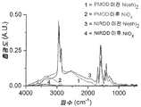
도 2는, 본 발명의 방법에 따른 니켈 전구체의 니켈 산화물로의 분해를 모니터링하는 적외선 스펙트럼을 도시한다.
도 3은, 본 발명에 따른 UV 광 분해 및 NIRDD 방법에 의해 준비된 니켈 산화물의 순환전 전압전류도(cyclic voltammograms)를 도시한다.
도 4의 a는, 본 발명에 따른, FTO 유리 상에 WCl6의 에탄올 용액을 퇴적하며, 그 다음에, UV 조사된 용액에 의한 무정형 텅스텐 산화물 막의 형성의 개략적인 도면이다.
도 4의 b 내지 e는 본 발명에 따라 준비된 무정형 텅스텐 산화물 막을 특징화한 결과를 도시하며, (b) FTO 유리 상의 WCl6에 대한 염소 함량을 판정하는 XRF 분석, (c) 및 (d) FTO 유리 상의 금속 산화물 막의 XPS 분석, 및 (e) 광분해 이전(프레시), UV 조사 이후, 및 어닐링 단계 이후 FTO 유리의 WCl3 막의 IR 스펙트럼을 포함한다.
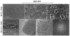
도 5는 본 발명의 실시예에 따라 준비된 a-WO3 막의 전자 현미경 사진을 도시한다.
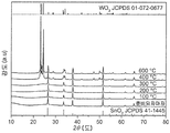
도 6은, 본 발명의 실시예에 따라 준비되며, 600℃까지 점진적으로 더 높은 온도에서 어닐링된 FTO 유리 상의 WO3의 박막의 XRD 회절도(diffractogram)를 도시한다.
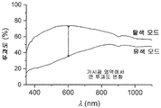
도 7은, 본 발명의 실시예에 따라 준비되는 텅스텐 산화물 막의 탈색 및 유색 상태에 대한 투과도 데이터를 도시한다.
도 8은, 본 발명의 실시예에 따라 준비되는 무정형 및 결정형 WO3의 전기 변색성에 관한 데이터를 도시한다.
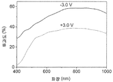
도 9는, 본 발명의 실시예에 따라 준비되는 니켈 산화물의 탈색 및 유색 상태에 대한 투과도 데이터를 도시한다.
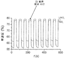
도 10은, 본 발명의 실시예에 따라 준비되는 니켈 산화물 막의 100 주기 동안의 전압 순환(cycling) 및 안정성을 도시하는 도면이다.
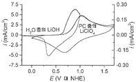
도 11은 물(H20) 및 비수 용매(PC-프로필렌 카보네이트) 중에서에 대한 본 발명의 실시예에 따라 준비되는 니켈 산화물 막의 순환 전압전류도를 도시한다.
도 12는, 순환 이벤트 동안 본 발명의 실시예에 따라 준비된 니켈 산화물 및 리튬 니켈 산화물 막에 대한 투과도 데이터를 도시한다.
도 13은 본 발명의 실시예에 따라 준비된 무정형 바나듐 산화물 막의 특징화에 관한 데이터를 도시하며, (a) FTO 유리 상의 VCl3에 대한 염소 함량을 판정하는 XRF 분석, (b) 및 (c) FTO 유리 상의 금속 산화물 막의 XPS 분석, 및 (d) 광분해 이전(프레시), UV 조사 이후, 및 어닐링 단계 이후 FTO 유리의 VCl3 막의 IR 스펙트럼을 포함한다.
도 14는, 본 발명의 실시예에 따라 준비된 바나듐 산화물 막의 탈색 및 유색 상태에 대한 투과도 데이터를 도시한다.
도 15는 본 발명의 실시예에 따라 준비된 무정형 니오븀 산화물 막의 특징화에 관한 데이터를 도시하며, (a) FTO 유리 상의 NbCl5에 대한 염소 함량을 판정하는 XRF 분석, (b) 및 (c) FTO 유리 상의 금속 산화물 막의 XPS 분석, 및 (d) 광분해 이전(프레시), UV 조사 이후, 및 어닐링 단계 이후 FTO 유리의 NbCl5 막의 IR 스펙트럼을 포함한다.
도 16은, 본 발명의 실시예에 따라 준비된 니오븀 산화물 막의 탈색 및 유색 상태에 대한 투과도 데이터를 도시한다.
도 17은 본 발명에 따라 준비된 무정형 몰리브덴 산화물 막의 특징화에 관한 데이터를 도시하며, (a) FTO 유리 상의 MoCl5에 대한 염소 함량을 판정하는 XRF 분석, (b) 및 (c) FTO 유리 상의 금속 산화물 막의 XPS 분석, 및 (d) 광분해 이전(프레시), UV 조사 이후, 및 어닐링 단계 이후 FTO 유리의 MoCl5 막의 IR 스펙트럼을 포함한다.
도 18은, 본 발명의 실시예에 따라 준비된 몰리브덴 산화물 막의 탈색 및 유색 상태에 대한 투과도 데이터를 도시한다.
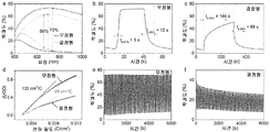
도 19는, (a) 준비되자마자의 WO3; (b) 1시간 동안 공기 중에서 200℃로 어닐링된 WO3; 및 (c) 1시간 동안 공기 중에서 600℃로 어닐링되는 WO3와 조립되는 디바이스의 ΔT, tb,90% 및 tc,90% 및 CE의 판정에 관한 데이터를 도시한다.
도 20a는, 지시된 전위에서 형성된 유색 및 탈색 상태에서, (각각 100℃에서 어닐링되며) 본 발명에 따라 준비된 V2O5, Nb2O5 또는 MoO3 능동 층을 포함하는 전기 변색 디바이스에 대한 광학 투과도 스펙트럼에 관한 데이터를 도시한다.
도 20b는, 본 발명에 따라 준비된 V2O5, Nb2O5 또는 MoO3 능동 층을 포함하는 전기 변색 디바이스에 대한 전하 밀도의 함수로서의 Δ(OD)의 변화에 관한 데이터를 도시한다.
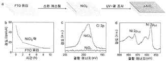
도 21a는 본 발명에 따른, FTO 유리 상에 NiCl2의 에탄올 용액을 퇴적하며, 그 다음에, UV 조사된 용액에 의한 무정형 니켈 산화물 막의 형성의 개략적인 도면이다.
도 21b 내지 도 21d는 본 발명에 따라 준비된 NiOX 막을 특징화한 결과를 도시하며, (b) 시간의 함수로서 염소 함량을 판정하는 XRF 분석, (c) 및 (d) FTO 유리 상의 금속 산화물 막의 XPS 분석을 포함한다.
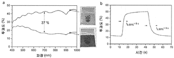
도 22a는, 본 발명의 실시예에 따라 준비된, 이온 저장 소재로서 FTO 유리 상대 전극 상의 NiOX 막을 사용하는 고체 상태 EC 디바이스의 아키텍쳐의 개략적인 도시이다.
도 22b 내지 도 22d는 본 발명에 따라 준비된 상대 전극 상에 NiOX 막을 이용하는 고체 상태 디바이스를 특징화한 결과를 도시하며, (b) FTO 유리 상대 전극 상에 a-NiOX를 갖고 및 갖지 않고 준비된 EC 디바이스에 대해 획득한 투과도 스펙트럼의 비교, (c) 상대 전극으로서 FTO 상에 a-NiOX를 갖고 준비된 EC 디바이스에 대한 시간의 함수로서의 투과도 변화, 및 (d) FTO 유리 상대 전극 상에 a-NiOX를 사용하여 준비된 고체 상태 EC 디바이스에 대한 전하 밀도 함수로서의 633nm에서의 광학 밀도의 변화를 포함한다.
도 23은, 본 발명의 실시예에 따라 준비된, 상대 전극으로서 무정형 및 결정형 니켈 산화물을 사용하는 EC 디바이스의 성능을 특징화하며 비교한 결과를 도시한다.
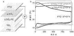
도 24a는, 본 발명의 실시예에 따라 준비된, 이온 저장 소재로서 FTO 유리 상대 전극 상의 TiO2 막을 이용하는 디바이스의 개략적인 도시이다.
도 24b는, 이온 저장 소재로서 FTO 유리 상대 전극 상의 TiO2 막을 이용하는 EC 디바이스를 특정화하며 비교하는 결과를 도시하며, (b) 전기 변색 층으로서 WO3를 가지며, 상대 전극으로서 FTO 상에 퇴적되는 a-TiO2(밝은 회색) 또는 결정형 c-TiO2(짙은 회색)을 갖거나, TiOX 막을 갖지 않는 EC 디바이스에 대한 1000 주기 동안의 700nm의 파장에서의 최대 및 최소 투과도를 포함한다.
도 25는, 본 발명에 따라 준비된 상이한 두께의 WO3 막을 특징화하는 결과를 도시한다.
도 26은, 본 발명에 따라 준비된 주석-도핑된 인듐 산화물(ITO)로 코팅된 폴리에틸렌 테레프탈레이트(PET) 상의 WO3 막에 대한 투과도 데이터를 도시한다.
도 27은, 본 발명에 따라 준비된 FTO 유리 상의 도핑되지 않은 WO3와 Nb-도핑된 WO3 막에 대한 투과도 데이터를 도시한다.
도 28은, 본 발명에 따라 준비된 FTO 유리 상의 도핑되지 않은 WO3와 Ti-도핑된 WO3 막에 대한 투과도 데이터를 도시한다.

| 능동 층 | 설명 | 준비 방법 | CE(cm2/C) | 파장a (nm) |
참고문헌 |
| 무정형 WO 3 | 600nm 무정형 막 | 광분해 | 133 | 700 | 본 문헌 |
| 결정형 WO 3 | 600nm 결정형 막 | 광분해 | 69 | 700 | 본 문헌 |
| WO3 | 무정형 막 | 전기 화학 퇴적 | 62 | 630 | Srivastava 등(2005) |
| WO3·2H20 | 결정형 나노시트 | 화학 솔루션 | 121 | 700 | Liang 등(2013) |
| WO3 | 결정형 나노와이어 | 열수 | 103 | 630 | Zhang 등(2011) |
| WO3 | 결정형 다공성소재 | 화학 응축 | 40 | 630 | Brezesinski 등(2006) |
| V 2 O 5 | 무정형 막 | 광분해 | 36 | 450 | 본 문헌 |
| V2O5 | 결정형 | 전기 화학 퇴적 | 36 | 430 | Scherer 등(2012) |
| V2O5 | 결정형 나노섬유 | 전기 화학 퇴적 | 32 | 450 | Tong 등(2015) |
| Nb 2 O 5 | 무정형 | 광분해 | 22 | 500 | 본 문헌 |
| Nb2O5 | 무정형 | 화학 응축 | 29 | 500 | Llordes 등(2016) |
| Nb2O5 | 무정형 | 열 응축 | 15 | 500 | Llordes 등(2016) |
| MoO3 | 무정형 | 광분해 | 57 | 550 | 본 문헌 |
| MoO3 | 무정형 | 화학 증기 퇴적 | 26 | 550 | Maruyama 등(1995) |
| MoO3 | 결정형 나노입자 | 졸-겔 | 24 | 550 | Hsu 등(2008) |
| 어닐링 온도 (℃) |
ΔT (%) |
tc,90% (s) |
tb,90% (s) |
CE (cm2/C) |
| 준비되지마자 | 60 | 15 | 4 | 92 |
| 100 | 70 | 12 | 5 | 133 |
| 200 | 66 | 14 | 6 | 131 |
| 400 | 56 | 68 | 166 | 69 |
| 600 | 42 | 101 | 109 | 69 |
| # 층b | ΔT (%) |
tb,90% (s) |
tc,90% (s) |
CE (cm2/C) |
| 1 | 29 | 2 | 2 | 193 |
| 3 | 55 | 9 | 3 | 153 |
| 5 | 70 | 12 | 5 | 133 |
| 7 | 68 | 28 | 13 | 118 |
| 10 | 62 | 24 | 23 | 117 |
| 상대 전극 | 순환 이전의 저항(Ω) | 1000 주기 이후의 저항(Ω) |
| FTO | 35 | 378 |
| FTO 상의 a-TiO2 | 32 | 33 |
| 상대 전극 소재 | 상 | 퇴적 방법 | ΔTa(%) | tc,90% b (s) |
tb,90% c (s) |
CEd (cm2/C) |
참고문헌 |
| NiO 다공성 막 | 결정형 | 화학욕 퇴적 | 55% | 10 | 20 | 87.2 | Zhang 등e |
| Nio 나노입자 막 | 결정형 | 잉크젯 인쇄 | 75% | 10 | 13 | 131.9 | Cai 등f |
| NiOX 막 | 결정형 | 마그네트론 스퍼터링 |
52% | 5 | 2 | - | Liu 등g |
| NiO 막 | 무정형 | UV | 60% | 4 | 6 | 141.1 | 본 작업 h |
| Nio 막 | 결정형 | UV | 26% | 78 | 17 | 72.0 | 본 작업 h |
Claims (29)
- 전기 변색 디바이스에 사용하기 위한 전기 변색 소재로서, 상기 전기 변색 소재는 전기 변색 금속 산화물 막으로 코팅된 투명 전도성 기판을 포함하며, 상기 전기 변색 금속 산화물 막은:
a) 상기 투명 전도성 기판을 제공하는 단계;
b) 하나 이상의 금속 전구체의 용액으로 상기 투명 전도성 기판을 코팅하는 단계; 및
c) 상기 투명 전도성 기판 상에서 상기 하나 이상의 금속 전구체를 상기 전기 변색 금속 산화물 막으로 변환하여, 상기 전기 변색 소재를 형성하도록, 상기 코팅된 투명 전도성 기판을 산소 분위기에서 근적외선 방사선, UV 방사선 및/또는 오존에 노광하는 단계를 포함하는 공정에 의해 형성되는, 전기 변색 소재. - 청구항 1에 있어서, 상기 전기 변색 금속 산화물 막을 형성하기 위한 공정은 대략 50℃ 내지 대략 500℃의 온도에서 상기 전기 변색 금속 산화물 막을 어닐링하는 단계를 더 포함하는, 전기 변색 소재.
- 청구항 2에 있어서, 어닐링 공정은 1시간 동안 대략 100℃에서 실행되는, 전기 변색 소재.
- 청구항 1 내지 청구항 3 중 어느 한 항에 있어서, 상기 전기 변색 금속 산화물 막은 단일 금속 산화물, 혼합 금속 산화물 또는 도핑된 금속 산화물을 포함하는, 전기 변색 소재.
- 청구항 4에 있어서, 상기 전기 변색 금속 산화물 막은 NiOX, WO3, MoO3, TiO2, Ta2O5, V2O5, Nb2O5, CoO2, IrOX, MnO2, FeOX 및 그 조합으로 이루어진 그룹으로부터 선택되는 금속 산화물을 포함하는, 전기 변색 소재.
- 청구항 4에 있어서, 상기 전기 변색 금속 산화물 막은 WO3을 포함하는, 전기 변색 소재.
- 청구항 4에 있어서, 상기 전기 변색 금속 산화물 막은 LiNiOX, TiWOX 및 FeNiOX로부터 선택되는 혼합 금속 산화물을 포함하는, 전기 변색 소재.
- 청구항 4에 있어서, 금속 산화물은 도핑된 금속 산화물인, 전기 변색 소재.
- 청구항 8에 있어서, 상기 도핑된 금속 산화물은 Nb 도핑된 WO3 또는 Ti 도핑된 WO3인, 전기 변색 소재.
- 청구항 1에 있어서, 상기 금속 전구체는, 근적외선 방사선, UV 방사선 및/또는 오존에 노광되면 금속 산화물로 변환되는 금속 유도체(derivative)인, 전기 변색 소재.
- 청구항 1 내지 청구항 10 중 어느 한 항에 있어서, 상기 금속 전구체는 금속 염화물, 금속 2-에틸헥사노에이트 또는 금속 아세틸아세토네이트인, 전기 변색 소재.
- 청구항 1 내지 청구항 11 중 어느 한 항에 있어서, 상기 투명 전도성 기판은 전도성 소재로 형성되는, 전기 변색 소재.
- 청구항 1 내지 청구항 11 중 어느 한 항에 있어서, 상기 투명 전도성 기판은 전도성 막으로 코팅된 투명한 소재로 형성되는, 전기 변색 소재.
- 청구항 1 내지 청구항 11 중 어느 한 항에 있어서, 상기 투명 전도성 기판은 불소 주석 산화물(FTO), 인듐 주석 산화물(ITO) 또는 알루미늄 아연 산화물(AZO)로 코팅된 기판인, 전기 변색 소재.
- 청구항 1 내지 청구항 11 중 어느 한 항에 있어서, 상기 투명 전도성 기판은 인듐 주석 산화물(ITO) 코팅된 PET인, 전기 변색 소재.
- 청구항 1 내지 청구항 15 중 어느 한 항에 있어서, 단계 b) 및 c)는, 상기 전기 변색 금속 산화물 막의 원하는 두께를 달성할 때까지 반복되는, 전기 변색 소재.
- 청구항 1 내지 청구항 16 중 어느 한 항에 있어서, 상기 전기 변색 금속 산화물 막은 무정형 금속 산화물 막인, 전기 변색 소재.
- 청구항 1 내지 청구항 16 중 어느 한 항에 있어서, 상기 전기 변색 금속 산화물 막은 결정형 금속 산화물 막인, 전기 변색 소재.
- 전기 변색 디바이스로서,
(a) 청구항 1 내지 청구항 18 중 어느 한 항에 기재된 전기 변색 소재를 포함하는 제1 전극,
(b) 상대 전극, 및
(c) 상기 제1 전극과 상기 상대 전극 사이에 이온을 전도하기 위한 이온-전도체 층을 포함하는, 전기 변색 디바이스. - 청구항 19에 있어서, 상기 제1 전극은 무정형 WO3 막으로 코팅된 FTO인, 전기 변색 디바이스.
- 청구항 19 또는 청구항 20에 있어서, 상기 상대 전극은 베어(bare) FTO인, 전기 변색 디바이스.
- 청구항 19 또는 청구항 20에 있어서, 상기 상대 전극은, 청구항 1에 기재된 공정을 사용하여 준비된 금속 산화물 막으로 코팅된 FTO인, 전기 변색 디바이스.
- 청구항 22에 있어서, 상기 상대 전극은 NiOX로 코팅된 FTO인, 전기 변색 디바이스.
- 청구항 22에 있어서, 상기 상대 전극은 TiOX로 코팅된 FTO인, 전기 변색 디바이스.
- 청구항 19 내지 청구항 24 중 어느 한 항에 있어서, 상기 이온-전도체 층은 전해질 용액인, 전기 변색 디바이스.
- 청구항 26에 있어서, 상기 전해질 용액은 LiClO4 프로필렌 카보네이트 전해질 용액인, 전기 변색 디바이스.
- 청구항 19 내지 청구항 24 중 어느 한 항에 있어서, 상기 전기 변색 디바이스는 고체 상태 디바이스인, 전기 변색 디바이스.
- 청구항 27에 있어서, 상기 이온-전도체 층은 전해질 겔인, 전기 변색 디바이스.
- 청구항 27에 있어서, 상기 이온-전도체 층은 LiCl04-프로필렌 카보네이트-PMMA 겔 전해질인, 전기 변색 디바이스.
Applications Claiming Priority (3)
| Application Number | Priority Date | Filing Date | Title |
|---|---|---|---|
| US201762534785P | 2017-07-20 | 2017-07-20 | |
| US62/534,785 | 2017-07-20 | ||
| PCT/CA2018/050885 WO2019014776A1 (en) | 2017-07-20 | 2018-07-20 | PHOTODEPOSITION OF METAL OXIDES FOR ELECTROCHROMIC DEVICES |
Publications (2)
| Publication Number | Publication Date |
|---|---|
| KR20200047533A true KR20200047533A (ko) | 2020-05-07 |
| KR102724277B1 KR102724277B1 (ko) | 2024-11-01 |
Family
ID=65015290
Family Applications (1)
| Application Number | Title | Priority Date | Filing Date |
|---|---|---|---|
| KR1020207004856A Active KR102724277B1 (ko) | 2017-07-20 | 2018-07-20 | 전기 변색 디바이스용 금속 산화물의 광퇴적 |
Country Status (10)
| Country | Link |
|---|---|
| US (1) | US12384715B2 (ko) |
| EP (1) | EP3655496B1 (ko) |
| JP (1) | JP7548815B2 (ko) |
| KR (1) | KR102724277B1 (ko) |
| CN (1) | CN111630134A (ko) |
| CA (1) | CA3070511A1 (ko) |
| ES (1) | ES2975068T3 (ko) |
| HR (1) | HRP20240519T1 (ko) |
| PL (1) | PL3655496T3 (ko) |
| WO (1) | WO2019014776A1 (ko) |
Cited By (1)
| Publication number | Priority date | Publication date | Assignee | Title |
|---|---|---|---|---|
| KR20230065721A (ko) * | 2021-11-05 | 2023-05-12 | 영남대학교 산학협력단 | 비정질 결정질 이중상 wo₃전극 및 전기변색소자 |
Families Citing this family (24)
| Publication number | Priority date | Publication date | Assignee | Title |
|---|---|---|---|---|
| KR102201549B1 (ko) * | 2017-06-27 | 2021-01-12 | 주식회사 엘지화학 | 장식 부재 및 이의 제조방법 |
| KR102035907B1 (ko) * | 2017-12-15 | 2019-10-23 | 주식회사 엘지화학 | 장식 부재 및 이의 제조방법 |
| CN108417179B (zh) * | 2018-05-16 | 2023-12-05 | 京东方科技集团股份有限公司 | 发光器件及显示装置 |
| WO2020005965A1 (en) * | 2018-06-25 | 2020-01-02 | The Regents Of The University Of California | Optically-transparent, thermally-insulating nanoporous coatings and monoliths |
| CN108663868B (zh) * | 2018-07-05 | 2021-01-05 | 东华大学 | 一种氧化钨电致变色电极的制备方法 |
| WO2020051419A1 (en) | 2018-09-06 | 2020-03-12 | Ambilight, Inc | Minimally color changing n-type ion storage layers, eletrochromic devices made therewith, and related methods |
| CN110488551A (zh) * | 2019-08-23 | 2019-11-22 | 南京邮电大学 | 一种柔性电致变色氧化物薄膜、器件及其制备方法 |
| CN111943523B (zh) * | 2020-08-24 | 2022-08-09 | 上海第二工业大学 | 一种五氧化二铌电致变色薄膜、水热合成方法及其用途 |
| CN114901596B (zh) * | 2020-08-26 | 2024-01-30 | 安比莱特 | 用作电致变色器件的电荷平衡材料的具有vox分子式的氧化钒 |
| CN113277744B (zh) * | 2021-05-28 | 2023-01-24 | 哈尔滨工业大学 | 一种用溶剂调控氧化镍电致变色薄膜形貌的方法 |
| CN113548809B (zh) * | 2021-08-12 | 2022-09-06 | 合肥工业大学 | 一种NiOx电致变色多孔材料及其制备方法 |
| CN113621270B (zh) * | 2021-08-27 | 2022-10-11 | 合肥工业大学 | 一种氧化镍纳米晶电致变色油墨的制备方法及其用途 |
| WO2023102643A1 (en) * | 2021-12-06 | 2023-06-15 | Miru Smart Technologies Corp. | Method of manufacturing curved electrochromic devices |
| CN114716155A (zh) * | 2022-03-24 | 2022-07-08 | 厦门理工学院 | 用于电致变色器件薄膜电极的制备方法、薄膜电极及用途 |
| CN114933420B (zh) * | 2022-05-31 | 2024-05-31 | 中国人民解放军火箭军工程大学 | 基于梯度温度的多层纳米片NiO电致变色薄膜水热制备方法 |
| CN114911106B (zh) * | 2022-06-02 | 2023-08-11 | 延安大学 | 核壳型五氧化二钒-三氧化钨@三氧化钼纳米花状电致变色薄膜的制备方法 |
| CN114994999B (zh) * | 2022-07-12 | 2023-08-25 | 延安大学 | 核壳型氧化锌@三氧化钨@三氧化钼Eu QDs纳米片微晶电极材料的制备方法 |
| CN116253525B (zh) * | 2022-11-24 | 2025-01-24 | 上海理工大学 | 一种二水合氧化钨电致变色纳米薄膜及其恒流电沉积制备方法 |
| CN115903323B (zh) * | 2022-12-12 | 2025-10-03 | 南京航空航天大学 | 一种超大变发射、透过率叠层电致变色器件及制备方法 |
| CN116083865B (zh) * | 2022-12-30 | 2025-04-04 | 常州大学 | 一种提高非晶wo3薄膜光学透过率的方法 |
| TWI855504B (zh) * | 2023-01-13 | 2024-09-11 | 南臺學校財團法人南臺科技大學 | 使具有金屬氧化物、銀及金屬氧化物之透明導電薄膜提高透光率與降低片電阻的方法 |
| CN116088240A (zh) * | 2023-02-13 | 2023-05-09 | 辽宁大学 | 基于多金属氧酸盐和钴掺杂二氧化锰的高性能电致变色-能量存储器件 |
| CN116835653B (zh) * | 2023-07-07 | 2025-07-01 | 浙江大学宁波“五位一体”校区教育发展中心 | 一种wo3@ito异质结纳米复合材料及其制备方法 |
| CN117364465B (zh) * | 2023-09-18 | 2026-04-24 | 武汉纺织大学 | 无机掺杂型电致变色织物及其制备方法 |
Citations (3)
| Publication number | Priority date | Publication date | Assignee | Title |
|---|---|---|---|---|
| KR20110057257A (ko) * | 2008-10-21 | 2011-05-31 | 도꾸리쯔교세이호진 상교기쥬쯔 소고겡뀨죠 | 금속 산화물 박막의 제조 방법 |
| KR20120085242A (ko) * | 2009-07-22 | 2012-07-31 | 세이지 일렉트로크로믹스, 인크. | 전기변색 장치 |
| KR20170063749A (ko) * | 2014-11-07 | 2017-06-08 | 플란제 에스이 | 금속산화물 박막, 금속산화물 박막을 증착하기 위한 방법 및 금속산화물 박막을 포함하는 장치 |
Family Cites Families (44)
| Publication number | Priority date | Publication date | Assignee | Title |
|---|---|---|---|---|
| US3669724A (en) | 1970-09-28 | 1972-06-13 | Motorola Inc | Method of vapor depositing a tungsten-tungsten oxide coating |
| JPS58110444A (ja) | 1981-12-18 | 1983-07-01 | Alps Electric Co Ltd | 着色金属酸化物皮膜の形成方法 |
| US4996083A (en) * | 1987-02-19 | 1991-02-26 | Donnelly Corporation | Method for deposition of electrochromic layers |
| US5034246A (en) | 1990-08-15 | 1991-07-23 | General Motors Corporation | Method for forming tungsten oxide films |
| GB9027608D0 (en) | 1990-12-20 | 1991-02-13 | Oxford Polytechnic | Making electrochromic films |
| GB9104377D0 (en) | 1991-03-01 | 1991-04-17 | Tseung Alfred C C | Depositing an electrochromic layer |
| US5384157A (en) | 1991-12-20 | 1995-01-24 | Fuji Xerox Co., Ltd. | Tungsten oxide film, process for producing same and electrochromic device using same |
| US6133050A (en) * | 1992-10-23 | 2000-10-17 | Symetrix Corporation | UV radiation process for making electronic devices having low-leakage-current and low-polarization fatigue |
| US5384653A (en) * | 1992-11-06 | 1995-01-24 | Midwest Research Institute | Stand-alone photovoltaic (PV) powered electrochromic window |
| US5661092A (en) * | 1995-09-01 | 1997-08-26 | The University Of Connecticut | Ultra thin silicon oxide and metal oxide films and a method for the preparation thereof |
| DE19548623A1 (de) | 1995-12-23 | 1997-06-26 | Hoechst Ag | 2-Acylamino-9-aryl-acridine, Verfahren zu ihrer Herstellung und diese enthaltende lichtempfindliche Gemische |
| US5825526A (en) * | 1996-04-24 | 1998-10-20 | Minnesota Mining And Manufacturing Company | Tape for use in manufacturing electrochromic devices |
| US5772978A (en) | 1996-04-24 | 1998-06-30 | Minnesota Mining And Manufacturing Company | Process for producing tungsten oxide |
| GB2326636B (en) * | 1997-06-28 | 2000-11-01 | Secr Defence | Sol-Gel route to transparent metal oxide films |
| US6582972B1 (en) * | 2000-04-07 | 2003-06-24 | Symetrix Corporation | Low temperature oxidizing method of making a layered superlattice material |
| US20020047148A1 (en) * | 2000-07-06 | 2002-04-25 | Won Seok-Jun | Methods of manufacturing integrated circuit capacitors having ruthenium upper electrodes and capacitors formed thereby |
| US6969539B2 (en) * | 2000-09-28 | 2005-11-29 | President And Fellows Of Harvard College | Vapor deposition of metal oxides, silicates and phosphates, and silicon dioxide |
| US6859297B2 (en) | 2001-08-07 | 2005-02-22 | Midwest Research Institute | Electrochromic counter electrode |
| US20040266211A1 (en) * | 2003-02-28 | 2004-12-30 | Board Of Regents, The University Of Texas System | Semiconductor interfaces |
| CN1305997C (zh) | 2004-03-10 | 2007-03-21 | 复旦大学 | 一种具有优良电致变色性能的金属氧化物介孔材料及其制备方法 |
| US7372610B2 (en) | 2005-02-23 | 2008-05-13 | Sage Electrochromics, Inc. | Electrochromic devices and methods |
| JP4864983B2 (ja) | 2006-01-09 | 2012-02-01 | エルジー・ケム・リミテッド | リチウムニッケル酸化物層を含む電極、その製造方法及びこれを含むエレクトロクロミック素子 |
| FR2911130B1 (fr) * | 2007-01-05 | 2009-11-27 | Saint Gobain | Procede de depot de couche mince et produit obtenu |
| WO2010107795A1 (en) * | 2009-03-17 | 2010-09-23 | Konarka Technologies, Inc. | Metal substrate for a dye sensitized photovoltaic cell |
| US9664974B2 (en) * | 2009-03-31 | 2017-05-30 | View, Inc. | Fabrication of low defectivity electrochromic devices |
| US8802201B2 (en) * | 2009-08-14 | 2014-08-12 | Asm America, Inc. | Systems and methods for thin-film deposition of metal oxides using excited nitrogen-oxygen species |
| JP5306144B2 (ja) | 2009-10-28 | 2013-10-02 | 三菱電機株式会社 | 電力開閉装置の開閉極時間測定装置 |
| US20110260124A1 (en) * | 2010-04-23 | 2011-10-27 | Alliance For Sustainable Energy, Llc | Alkali metal ion-doped electrochromic films and methods of making the same |
| US8753987B2 (en) | 2010-06-08 | 2014-06-17 | Sumitomo Metal Mining Co., Ltd. | Method of manufacturing metal oxide film |
| US8894827B2 (en) | 2011-01-18 | 2014-11-25 | Applied Materials, Inc. | Electrochromic tungsten oxide film deposition |
| US8780432B1 (en) * | 2011-03-22 | 2014-07-15 | Paul Phong Nguyen | Electrochromic devices and methods for forming such devices |
| CN107300819B (zh) * | 2011-07-21 | 2021-03-12 | Sage电致变色显示有限公司 | 同时掺杂有锂和金属掺杂物的电致变色的镍氧化物 |
| HK1201102A1 (en) | 2011-07-25 | 2015-08-21 | 加州大学校务委员会 | Electrochromic nanocomposite films |
| JPWO2013141375A1 (ja) | 2012-03-22 | 2015-08-03 | 大日本印刷株式会社 | 熱線制御シート |
| EP3543781B1 (en) | 2012-08-09 | 2022-10-12 | SAGE Electrochromics, lnc. | Lithium metal oxide materials for electrochromic devices |
| ES2733281T3 (es) | 2013-01-21 | 2019-11-28 | Kinestral Tech Inc | Dispositivo electrocromático multicapa con ánodo a base de óxido de litio y níquel |
| JP6117124B2 (ja) * | 2013-03-19 | 2017-04-19 | 富士フイルム株式会社 | 酸化物半導体膜及びその製造方法 |
| US20150225845A1 (en) * | 2014-02-12 | 2015-08-13 | Electronics And Telecommunications Research Institute | Method for forming metal oxide thin film and device for printing metal oxide thin film |
| WO2016033211A2 (en) * | 2014-08-27 | 2016-03-03 | 3M Innovative Properties Company | Electrical multilayer lamination transfer films |
| TWI689622B (zh) * | 2014-12-05 | 2020-04-01 | 日商富士軟片股份有限公司 | 金屬氧化物膜的製造方法、金屬氧化物膜、薄膜電晶體、薄膜電晶體的製造方法、電子元件及紫外線照射裝置 |
| WO2016101067A1 (en) | 2014-12-22 | 2016-06-30 | Firewater Fuel Corp. | Electrocatalytic films comprising amorphous metals or metal-oxides prepared using near-infrared decomposition of precursors |
| US20180173071A1 (en) | 2015-07-10 | 2018-06-21 | View, Inc. | Bird friendly electrochromic devices |
| EP3347929B1 (en) * | 2015-09-08 | 2021-01-06 | Yeda Research and Development Co. Ltd. | Methods of preparing multilayered electrochromic systems |
| KR101830873B1 (ko) | 2015-10-05 | 2018-02-21 | 영남대학교 산학협력단 | 다공성 지지체를 이용한 스마트 윈도우의 제조방법 |
-
2018
- 2018-07-20 CA CA3070511A patent/CA3070511A1/en active Pending
- 2018-07-20 HR HRP20240519TT patent/HRP20240519T1/hr unknown
- 2018-07-20 JP JP2020524658A patent/JP7548815B2/ja active Active
- 2018-07-20 EP EP18834936.9A patent/EP3655496B1/en active Active
- 2018-07-20 PL PL18834936.9T patent/PL3655496T3/pl unknown
- 2018-07-20 KR KR1020207004856A patent/KR102724277B1/ko active Active
- 2018-07-20 CN CN201880048500.9A patent/CN111630134A/zh active Pending
- 2018-07-20 WO PCT/CA2018/050885 patent/WO2019014776A1/en not_active Ceased
- 2018-07-20 US US16/632,636 patent/US12384715B2/en active Active
- 2018-07-20 ES ES18834936T patent/ES2975068T3/es active Active
Patent Citations (3)
| Publication number | Priority date | Publication date | Assignee | Title |
|---|---|---|---|---|
| KR20110057257A (ko) * | 2008-10-21 | 2011-05-31 | 도꾸리쯔교세이호진 상교기쥬쯔 소고겡뀨죠 | 금속 산화물 박막의 제조 방법 |
| KR20120085242A (ko) * | 2009-07-22 | 2012-07-31 | 세이지 일렉트로크로믹스, 인크. | 전기변색 장치 |
| KR20170063749A (ko) * | 2014-11-07 | 2017-06-08 | 플란제 에스이 | 금속산화물 박막, 금속산화물 박막을 증착하기 위한 방법 및 금속산화물 박막을 포함하는 장치 |
Cited By (1)
| Publication number | Priority date | Publication date | Assignee | Title |
|---|---|---|---|---|
| KR20230065721A (ko) * | 2021-11-05 | 2023-05-12 | 영남대학교 산학협력단 | 비정질 결정질 이중상 wo₃전극 및 전기변색소자 |
Also Published As
| Publication number | Publication date |
|---|---|
| EP3655496A1 (en) | 2020-05-27 |
| HRP20240519T1 (hr) | 2024-07-19 |
| WO2019014776A1 (en) | 2019-01-24 |
| PL3655496T3 (pl) | 2024-06-10 |
| ES2975068T3 (es) | 2024-07-03 |
| CN111630134A (zh) | 2020-09-04 |
| JP2020527760A (ja) | 2020-09-10 |
| JP7548815B2 (ja) | 2024-09-10 |
| US12384715B2 (en) | 2025-08-12 |
| CA3070511A1 (en) | 2019-01-24 |
| US20200165161A1 (en) | 2020-05-28 |
| EP3655496C0 (en) | 2023-12-27 |
| EP3655496A4 (en) | 2021-06-23 |
| KR102724277B1 (ko) | 2024-11-01 |
| EP3655496B1 (en) | 2023-12-27 |
Similar Documents
| Publication | Publication Date | Title |
|---|---|---|
| KR102724277B1 (ko) | 전기 변색 디바이스용 금속 산화물의 광퇴적 | |
| Choi et al. | Electrochromic performance of viologen-modified periodic mesoporous nanocrystalline anatase electrodes | |
| US8687261B2 (en) | Electrochromic nickel oxide simultaneously doped with lithium and a metal dopant | |
| US9798214B2 (en) | Methods of charging solid state plasmonic electrochromic smart window devices | |
| US10545387B2 (en) | Electrochromic device for applying voltage to electrodes | |
| JP7803930B2 (ja) | 動的光スループット制御を行うエレクトロクロミック二重層装置とその製造工程 | |
| Goei et al. | Nd–Nb Co-doped SnO2/α-WO3 electrochromic materials: enhanced stability and switching properties | |
| Fu et al. | Investigation of electrochromic device based on multi-step electrodeposited PB films | |
| KR102230604B1 (ko) | 광감응자동변색소자 및 그 제조방법 | |
| Wu et al. | Electrochromic materials: scope for the cyclic decay mechanisms and performance stability optimisation strategies | |
| Haritha et al. | Sol–gel derived ZnO thin film as a transparent counter electrode for WO3 based electrochromic devices | |
| KR20160084246A (ko) | 광전기 변색소자용 복합체 및 광전기 변색소자의 제조방법 | |
| Patel et al. | Highly Transparent Spectral Tunable Electrochromic Window Based on Solid‐State WO3 Thin Films | |
| US10877347B1 (en) | Thin film lithium tungsten oxides for electrochromic applications and methods of making the same | |
| HK40029824A (en) | Photodeposition of metal oxides for electrochromic devices | |
| JP4849844B2 (ja) | 色素増感太陽電池 | |
| LUO et al. | Green Energy and Resources | |
| 박재혁 | Preparation of Dip-coated Electrochromic Thin Film and Its Application to Photoelectrochromic Systems | |
| Liu et al. | Enhanced Coloration Efficiency of Electrochromic Thin Film Based on TiO2 and Chitosan | |
| Azens | Recent advances in electrochromics for smart windows applications | |
| H Almarri | Enhanced Electrochromic Properties of Anatase Tio2 for Flexible Electrochromic Device | |
| Kang et al. | Ultra‑Stable Wo3 Electrochromic Film Based on Nh4+ Hydrogen Bond Chemistry | |
| Jiao | Nanostructured electrochromic and photoelectrochemical materials and devices | |
| Buch et al. | Applied Science Letters |
Legal Events
| Date | Code | Title | Description |
|---|---|---|---|
| PA0105 | International application |
Patent event date: 20200219 Patent event code: PA01051R01D Comment text: International Patent Application |
|
| PG1501 | Laying open of application | ||
| A201 | Request for examination | ||
| PA0201 | Request for examination |
Patent event code: PA02012R01D Patent event date: 20210719 Comment text: Request for Examination of Application |
|
| E902 | Notification of reason for refusal | ||
| PE0902 | Notice of grounds for rejection |
Comment text: Notification of reason for refusal Patent event date: 20230417 Patent event code: PE09021S01D |
|
| E90F | Notification of reason for final refusal | ||
| PE0902 | Notice of grounds for rejection |
Comment text: Final Notice of Reason for Refusal Patent event date: 20240229 Patent event code: PE09021S02D |
|
| E701 | Decision to grant or registration of patent right | ||
| PE0701 | Decision of registration |
Patent event code: PE07011S01D Comment text: Decision to Grant Registration Patent event date: 20240731 |
|
| GRNT | Written decision to grant | ||
| PR0701 | Registration of establishment |
Comment text: Registration of Establishment Patent event date: 20241028 Patent event code: PR07011E01D |
|
| PR1002 | Payment of registration fee |
Payment date: 20241029 End annual number: 3 Start annual number: 1 |
|
| PG1601 | Publication of registration |