KR20200048205A - 플렉서블 회로 필름 및 이를 포함하는 전자 기기 - Google Patents
플렉서블 회로 필름 및 이를 포함하는 전자 기기 Download PDFInfo
- Publication number
- KR20200048205A KR20200048205A KR1020180130013A KR20180130013A KR20200048205A KR 20200048205 A KR20200048205 A KR 20200048205A KR 1020180130013 A KR1020180130013 A KR 1020180130013A KR 20180130013 A KR20180130013 A KR 20180130013A KR 20200048205 A KR20200048205 A KR 20200048205A
- Authority
- KR
- South Korea
- Prior art keywords
- film
- layer
- bending
- flexible circuit
- touch
- Prior art date
- Legal status (The legal status is an assumption and is not a legal conclusion. Google has not performed a legal analysis and makes no representation as to the accuracy of the status listed.)
- Granted
Links
Images


Classifications
-
- H—ELECTRICITY
- H05—ELECTRIC TECHNIQUES NOT OTHERWISE PROVIDED FOR
- H05K—PRINTED CIRCUITS; CASINGS OR CONSTRUCTIONAL DETAILS OF ELECTRIC APPARATUS; MANUFACTURE OF ASSEMBLAGES OF ELECTRICAL COMPONENTS
- H05K1/00—Printed circuits
- H05K1/02—Details
- H05K1/0277—Bendability or stretchability details
- H05K1/028—Bending or folding regions of flexible printed circuits
-
- H—ELECTRICITY
- H05—ELECTRIC TECHNIQUES NOT OTHERWISE PROVIDED FOR
- H05K—PRINTED CIRCUITS; CASINGS OR CONSTRUCTIONAL DETAILS OF ELECTRIC APPARATUS; MANUFACTURE OF ASSEMBLAGES OF ELECTRICAL COMPONENTS
- H05K1/00—Printed circuits
- H05K1/18—Printed circuits structurally associated with non-printed electric components
- H05K1/189—Printed circuits structurally associated with non-printed electric components characterised by the use of flexible or folded printed circuits
-
- H—ELECTRICITY
- H05—ELECTRIC TECHNIQUES NOT OTHERWISE PROVIDED FOR
- H05K—PRINTED CIRCUITS; CASINGS OR CONSTRUCTIONAL DETAILS OF ELECTRIC APPARATUS; MANUFACTURE OF ASSEMBLAGES OF ELECTRICAL COMPONENTS
- H05K1/00—Printed circuits
- H05K1/02—Details
- H05K1/0277—Bendability or stretchability details
- H05K1/028—Bending or folding regions of flexible printed circuits
- H05K1/0281—Reinforcement details thereof
-
- G—PHYSICS
- G06—COMPUTING OR CALCULATING; COUNTING
- G06F—ELECTRIC DIGITAL DATA PROCESSING
- G06F1/00—Details not covered by groups G06F3/00 - G06F13/00 and G06F21/00
- G06F1/16—Constructional details or arrangements
- G06F1/1613—Constructional details or arrangements for portable computers
- G06F1/1633—Constructional details or arrangements of portable computers not specific to the type of enclosures covered by groups G06F1/1615 - G06F1/1626
- G06F1/1637—Details related to the display arrangement, including those related to the mounting of the display in the housing
- G06F1/1652—Details related to the display arrangement, including those related to the mounting of the display in the housing the display being flexible, e.g. mimicking a sheet of paper, or rollable
-
- G—PHYSICS
- G06—COMPUTING OR CALCULATING; COUNTING
- G06F—ELECTRIC DIGITAL DATA PROCESSING
- G06F3/00—Input arrangements for transferring data to be processed into a form capable of being handled by the computer; Output arrangements for transferring data from processing unit to output unit, e.g. interface arrangements
- G06F3/01—Input arrangements or combined input and output arrangements for interaction between user and computer
- G06F3/03—Arrangements for converting the position or the displacement of a member into a coded form
- G06F3/041—Digitisers, e.g. for touch screens or touch pads, characterised by the transducing means
- G06F3/0412—Digitisers structurally integrated in a display
-
- H—ELECTRICITY
- H04—ELECTRIC COMMUNICATION TECHNIQUE
- H04M—TELEPHONIC COMMUNICATION
- H04M1/00—Substation equipment, e.g. for use by subscribers
- H04M1/02—Constructional features of telephone sets
- H04M1/0202—Portable telephone sets, e.g. cordless phones, mobile phones or bar type handsets
-
- H—ELECTRICITY
- H05—ELECTRIC TECHNIQUES NOT OTHERWISE PROVIDED FOR
- H05K—PRINTED CIRCUITS; CASINGS OR CONSTRUCTIONAL DETAILS OF ELECTRIC APPARATUS; MANUFACTURE OF ASSEMBLAGES OF ELECTRICAL COMPONENTS
- H05K1/00—Printed circuits
- H05K1/02—Details
- H05K1/14—Structural association of two or more printed circuits
- H05K1/147—Structural association of two or more printed circuits at least one of the printed circuits being bent or folded, e.g. by using a flexible printed circuit
-
- H—ELECTRICITY
- H05—ELECTRIC TECHNIQUES NOT OTHERWISE PROVIDED FOR
- H05K—PRINTED CIRCUITS; CASINGS OR CONSTRUCTIONAL DETAILS OF ELECTRIC APPARATUS; MANUFACTURE OF ASSEMBLAGES OF ELECTRICAL COMPONENTS
- H05K3/00—Apparatus or processes for manufacturing printed circuits
- H05K3/22—Secondary treatment of printed circuits
- H05K3/28—Applying non-metallic protective coatings
- H05K3/281—Applying non-metallic protective coatings by means of a preformed insulating foil
-
- H—ELECTRICITY
- H05—ELECTRIC TECHNIQUES NOT OTHERWISE PROVIDED FOR
- H05K—PRINTED CIRCUITS; CASINGS OR CONSTRUCTIONAL DETAILS OF ELECTRIC APPARATUS; MANUFACTURE OF ASSEMBLAGES OF ELECTRICAL COMPONENTS
- H05K3/00—Apparatus or processes for manufacturing printed circuits
- H05K3/38—Improvement of the adhesion between the insulating substrate and the metal
- H05K3/386—Improvement of the adhesion between the insulating substrate and the metal by the use of an organic polymeric bonding layer, e.g. adhesive
-
- H—ELECTRICITY
- H05—ELECTRIC TECHNIQUES NOT OTHERWISE PROVIDED FOR
- H05K—PRINTED CIRCUITS; CASINGS OR CONSTRUCTIONAL DETAILS OF ELECTRIC APPARATUS; MANUFACTURE OF ASSEMBLAGES OF ELECTRICAL COMPONENTS
- H05K3/00—Apparatus or processes for manufacturing printed circuits
- H05K3/46—Manufacturing multilayer circuits
-
- H—ELECTRICITY
- H05—ELECTRIC TECHNIQUES NOT OTHERWISE PROVIDED FOR
- H05K—PRINTED CIRCUITS; CASINGS OR CONSTRUCTIONAL DETAILS OF ELECTRIC APPARATUS; MANUFACTURE OF ASSEMBLAGES OF ELECTRICAL COMPONENTS
- H05K5/00—Casings, cabinets or drawers for electric apparatus
- H05K5/02—Details
- H05K5/03—Covers
-
- H—ELECTRICITY
- H05—ELECTRIC TECHNIQUES NOT OTHERWISE PROVIDED FOR
- H05K—PRINTED CIRCUITS; CASINGS OR CONSTRUCTIONAL DETAILS OF ELECTRIC APPARATUS; MANUFACTURE OF ASSEMBLAGES OF ELECTRICAL COMPONENTS
- H05K7/00—Constructional details common to different types of electric apparatus
- H05K7/20—Modifications to facilitate cooling, ventilating, or heating
- H05K7/20954—Modifications to facilitate cooling, ventilating, or heating for display panels
- H05K7/20963—Heat transfer by conduction from internal heat source to heat radiating structure
-
- H—ELECTRICITY
- H05—ELECTRIC TECHNIQUES NOT OTHERWISE PROVIDED FOR
- H05K—PRINTED CIRCUITS; CASINGS OR CONSTRUCTIONAL DETAILS OF ELECTRIC APPARATUS; MANUFACTURE OF ASSEMBLAGES OF ELECTRICAL COMPONENTS
- H05K2201/00—Indexing scheme relating to printed circuits covered by H05K1/00
- H05K2201/01—Dielectrics
- H05K2201/0137—Materials
- H05K2201/0154—Polyimide
-
- H—ELECTRICITY
- H05—ELECTRIC TECHNIQUES NOT OTHERWISE PROVIDED FOR
- H05K—PRINTED CIRCUITS; CASINGS OR CONSTRUCTIONAL DETAILS OF ELECTRIC APPARATUS; MANUFACTURE OF ASSEMBLAGES OF ELECTRICAL COMPONENTS
- H05K2201/00—Indexing scheme relating to printed circuits covered by H05K1/00
- H05K2201/10—Details of components or other objects attached to or integrated in a printed circuit board
- H05K2201/10007—Types of components
- H05K2201/10128—Display
Landscapes
- Engineering & Computer Science (AREA)
- Microelectronics & Electronic Packaging (AREA)
- Theoretical Computer Science (AREA)
- Manufacturing & Machinery (AREA)
- Physics & Mathematics (AREA)
- General Engineering & Computer Science (AREA)
- Computer Hardware Design (AREA)
- Human Computer Interaction (AREA)
- General Physics & Mathematics (AREA)
- Thermal Sciences (AREA)
- Signal Processing (AREA)
- Structure Of Printed Boards (AREA)
- Non-Metallic Protective Coatings For Printed Circuits (AREA)
Abstract
Description
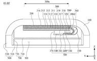
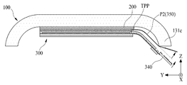
도 2는 도 1에 도시된 선 I-I'의 단면도이다.
도 3은 본 출원의 일 예에 따른 전자 기기를 나타내는 평면도이다.
도 4는 도 3에 도시된 커버 윈도우의 후면을 나타내는 도면이다.
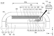
도 5는 도 3에 도시된 선 II-II'의 단면도이다.
도 6은 도 3에 도시된 선 III-III'의 단면도이다.
도 7은 도 3에 도시된 선 II-II'의 다른 단면도이다.
도 8a 내지 도 8c는 본 출원의 일 예에 따른 전자 기기에서, 커버 윈도우와 디스플레이 모듈의 본딩 공정과 디스플레이 모듈의 벤딩 공정을 나타내는 공정 순서도이다.
12: 회로 배선층 13: 커버층
14: 코팅층 15: 격벽
100: 커버 윈도우 200: 모듈 본딩 부재
300: 디스플레이 모듈 310: 플렉서블 기판
315: 터치 전극부 317: 제 1 백 플레이트
318: 제 2 백 플레이트 319: 방열부
320: 벤딩 유지 부재 340: 인쇄 회로 기판
350: 터치 플렉서블 회로 필름 360: 마이크로 커버층
370: PCB 고정 부재 380: 회로 필름 고정 부재
500: 하우징
Claims (20)
- 본딩 패드부;
몸체부; 및
상기 본딩 패드부와 상기 몸체부 사이의 필름 벤딩부를 포함하며,
상기 필름 벤딩부의 적어도 일부는 상기 몸체부의 두께보다 얇은 두께를 갖는, 플렉서블 회로 필름. - 제 1 항에 있어서,
상기 본딩 패드부와 상기 필름 벤딩부 및 상기 몸체부 각각은 복층 구조를 가지며,
상기 필름 벤딩부의 적어도 일부는 상기 몸체부보다 적은 층수를 갖는, 플렉서블 회로 필름. - 제 2 항에 있어서,
상기 필름 벤딩부의 적어도 일부는 4층 이하의 복층 구조를 가지며,
상기 몸체부는 5층 이상의 복층 구조를 갖는, 플렉서블 회로 필름. - 제 1 항에 있어서,
상기 본딩 패드부와 상기 필름 벤딩부 및 상기 몸체부를 갖는 베이스 부재;
상기 본딩 패드부와 상기 필름 벤딩부 및 상기 몸체부 각각의 상기 베이스 부재 상에 배치된 회로 배선층;
상기 몸체부 상에 배치된 상기 회로 배선층을 덮는 커버층; 및
상기 필름 벤딩부의 적어도 일부 상에 배치된 상기 회로 배선층을 덮는 코팅층을 포함하며,
상기 코팅층의 두께는 상기 커버층의 두께보다 얇은, 플렉서블 회로 필름. - 제 4 항에 있어서,
상기 코팅층의 두께는 5 마이크로미터 이상인, 플렉서블 회로 필름. - 제 4 항에 있어서,
상기 베이스 부재의 전면으로부터 상기 코팅층의 최상면까지의 제 1 높이는 상기 베이스 부재의 전면으로부터 커버층의 최상면까지의 제 2 높이보다 낮은, 플렉서블 회로 필름. - 제 4 항에 있어서,
상기 코팅층은 폴리이미드 물질 또는 솔더 레지스트 물질을 포함하는, 플렉서블 회로 필름. - 제 4 항에 있어서,
상기 필름 벤딩부에 접한 상기 본딩 패드부의 일측 상에 배치된 격벽을 더 포함하며,
상기 코팅층은 상기 필름 벤딩부에 접한 상기 격벽의 일측을 덮는, 플렉서블 회로 필름. - 제 8 항에 있어서,
상기 격벽은 상기 커버층과 동일한 물질로 이루어진, 플렉서블 회로 필름. - 커버 윈도우; 및
상기 커버 윈도우에 결합된 디스플레이 모듈을 포함하고,
상기 디스플레이 모듈은 터치 패드부에 본딩된 터치 플렉서블 회로 필름을 포함하며,
상기 터치 플렉서블 회로 필름은 청구항 1 내지 9 중 어느 한 항의 플렉서블 회로 필름을 포함하는, 전자 기기. - 제 10 항에 있어서,
상기 커버 윈도우는,
상기 디스플레이 모듈의 전면(前面)을 덮는 전면부; 및
상기 전면부의 후면 가장자리에 마련되어 상기 디스플레이 모듈의 각 측면을 감싸는 측벽부를 포함하는, 전자 기기. - 제 11 항에 있어서,
상기 측벽부는 상기 전면부 가자장리로부터 곡면 형태를 가지도록 만곡된, 전자 기기. - 제 11 항에 있어서,
상기 디스플레이 모듈은,
표시부, 곡면 형태로 벤딩된 패널 벤딩 영역, 및 상기 표시부와 중첩되는 디스플레이 패드부를 포함하는 플렉서블 기판;
상기 표시부 상에 배치된 화소 어레이부;
상기 화소 어레이부 상에 배치된 터치 전극부; 및
상기 디스플레이 패드부와 전기적으로 연결되고 상기 터치 플렉서블 회로 필름과 전기적으로 접속된 인쇄 회로 기판을 포함하며,
상기 터치 패드부는 상기 터치 전극부의 일측 가장자리 부분에 배치되어 상기 터치 전극부와 전기적으로 연결된, 전자 기기. - 제 13 항에 있어서,
상기 디스플레이 모듈은,
상기 화소 어레이부와 중첩되는 플렉서블 기판의 후면에 부착된 제 1 백 플레이트;
상기 디스플레이 패드부와 중첩되는 플렉서블 기판의 후면에 부착되고 상기 제 1 백 플레이트와 중첩되는 제 2 백 플레이트; 및
상기 제 1 백 플레이트와 상기 제 2 백 플레이트 사이에 배치된 벤딩 유지 부재를 더 포함하며,
상기 터치 플렉서블 회로 필름은 상기 제 1 백 플레이트와 상기 벤딩 유지 부재 및 상기 제 2 백 플레이트를 감싸도록 벤딩되어 상기 인쇄 회로 기판에 실장된 커넥터와 접속된, 전자 기기. - 제 14 항에 있어서,
상기 제 2 백 플레이트와 중첩되는 상기 마이크로 커버층과 상기 터치 플렉서블 회로 필름 사이에 배치된 회로 필름 고정 부재를 더 포함하며,
상기 터치 플렉서블 회로 필름은 상기 회로 필름 고정 부재에 의해 상기 마이크로 커버층에 고정된, 전자 기기. - 제 14 항에 있어서,
상기 제 1 백 플레이트의 후면에 부착된 방열부를 더 포함하며,
상기 벤딩 유지 부재는 상기 방열부와 상기 제 2 백 플레이트 사이에 배치된, 전자 기기. - 제 16 항에 있어서,
상기 벤딩 유지 부재는 양면 테이프인, 전자 기기. - 제 14 항에 있어서,
상기 제 1 백 플레이트의 후면에 부착된 방열부; 및
상기 인쇄 회로 기판을 상기 방열부에 고정시키는 PCB 고정 부재를 더 포함하는, 전자 기기. - 제 18 항에 있어서,
상기 PCB 고정 부재는 전도층을 포함하는, 전자 기기. - 제 18 항에 있어서,
상기 벤딩 유지 부재는 상기 방열부와 상기 제 2 백 플레이트 사이에 배치된, 전자 기기.
Priority Applications (2)
| Application Number | Priority Date | Filing Date | Title |
|---|---|---|---|
| KR1020180130013A KR102703682B1 (ko) | 2018-10-29 | 2018-10-29 | 플렉서블 회로 필름 및 이를 포함하는 전자 기기 |
| US16/568,745 US11129281B2 (en) | 2018-10-29 | 2019-09-12 | Flexible circuit film and electronic device comprising the same |
Applications Claiming Priority (1)
| Application Number | Priority Date | Filing Date | Title |
|---|---|---|---|
| KR1020180130013A KR102703682B1 (ko) | 2018-10-29 | 2018-10-29 | 플렉서블 회로 필름 및 이를 포함하는 전자 기기 |
Publications (2)
| Publication Number | Publication Date |
|---|---|
| KR20200048205A true KR20200048205A (ko) | 2020-05-08 |
| KR102703682B1 KR102703682B1 (ko) | 2024-09-04 |
Family
ID=70326276
Family Applications (1)
| Application Number | Title | Priority Date | Filing Date |
|---|---|---|---|
| KR1020180130013A Active KR102703682B1 (ko) | 2018-10-29 | 2018-10-29 | 플렉서블 회로 필름 및 이를 포함하는 전자 기기 |
Country Status (2)
| Country | Link |
|---|---|
| US (1) | US11129281B2 (ko) |
| KR (1) | KR102703682B1 (ko) |
Cited By (4)
| Publication number | Priority date | Publication date | Assignee | Title |
|---|---|---|---|---|
| WO2022030915A1 (ko) * | 2020-08-04 | 2022-02-10 | 삼성전자 주식회사 | 디스플레이 구동 회로의 방열 특성을 높일 수 있는 전자 장치 |
| US11856741B2 (en) | 2020-08-24 | 2023-12-26 | Lg Display Co., Ltd. | Display module and display device |
| US12063764B2 (en) | 2020-12-18 | 2024-08-13 | Samsung Display Co., Ltd. | Heat dissipation layer and display device including the same |
| WO2025048309A1 (ko) * | 2023-08-28 | 2025-03-06 | 삼성전자 주식회사 | 플렉서블 접속 부재 및 이를 포함하는 전자 장치 |
Families Citing this family (12)
| Publication number | Priority date | Publication date | Assignee | Title |
|---|---|---|---|---|
| CN109739386B (zh) * | 2019-01-08 | 2021-10-15 | 京东方科技集团股份有限公司 | 触控传感器、触控模组及触控传感器裂纹检测方法 |
| KR102622729B1 (ko) * | 2019-06-20 | 2024-01-11 | 삼성디스플레이 주식회사 | 표시 장치 |
| KR20210049326A (ko) | 2019-10-25 | 2021-05-06 | 엘지디스플레이 주식회사 | 플렉서블 표시 장치 |
| KR102925181B1 (ko) * | 2020-01-10 | 2026-02-09 | 삼성디스플레이 주식회사 | 표시 장치 |
| CN111580699B (zh) * | 2020-05-13 | 2023-10-24 | 京东方科技集团股份有限公司 | 显示模组及显示装置 |
| CN112599019B (zh) * | 2021-01-05 | 2023-01-10 | 武汉华星光电半导体显示技术有限公司 | 显示装置 |
| CN115174715A (zh) * | 2021-06-30 | 2022-10-11 | Oppo广东移动通信有限公司 | 柔性显示屏支撑片、柔性显示屏及电子设备 |
| CN114245582B (zh) * | 2021-12-16 | 2024-09-20 | 林淡钦 | 一种柔性电路板加工制造设备 |
| KR20230094215A (ko) * | 2021-12-20 | 2023-06-28 | 삼성디스플레이 주식회사 | 표시 장치 |
| KR20230099119A (ko) * | 2021-12-27 | 2023-07-04 | 엘지디스플레이 주식회사 | 표시 모듈 및 표시 장치 |
| CN115914447B (zh) * | 2022-09-27 | 2025-05-27 | 星源电子科技(深圳)有限公司 | 一种具备高跌落强度的设备 |
| CN118553156A (zh) | 2023-02-24 | 2024-08-27 | 北京小米移动软件有限公司 | 电子设备 |
Citations (2)
| Publication number | Priority date | Publication date | Assignee | Title |
|---|---|---|---|---|
| KR101092987B1 (ko) * | 2011-08-03 | 2011-12-12 | 주식회사 플렉스컴 | 절곡부를 갖는 연성회로기판 및 그의 제조방법 |
| KR20170071986A (ko) * | 2015-12-16 | 2017-06-26 | 엘지디스플레이 주식회사 | 플렉서블 디스플레이 장치 |
Family Cites Families (10)
| Publication number | Priority date | Publication date | Assignee | Title |
|---|---|---|---|---|
| KR20070012077A (ko) | 2005-07-22 | 2007-01-25 | 삼성전자주식회사 | 연성 인쇄회로기판 및 이를 포함하는 액정표시장치 |
| CN100501177C (zh) * | 2006-06-23 | 2009-06-17 | 鸿富锦精密工业(深圳)有限公司 | 铰链结构及应用该铰链结构的折叠式电子装置 |
| EP2129194B1 (en) * | 2008-05-27 | 2013-08-07 | VIA Technologies, Inc. | Electronic apparatus |
| US9419065B2 (en) * | 2012-08-07 | 2016-08-16 | Apple Inc. | Flexible displays |
| US9349969B2 (en) * | 2013-02-01 | 2016-05-24 | Lg Display Co., Ltd. | Electronic devices with flexible display and method for manufacturing the same |
| US9933870B2 (en) * | 2015-03-17 | 2018-04-03 | Lg Display Co., Ltd. | Back plate member for flexible display, display apparatus including the same, and method of manufacturing the same |
| CN204884440U (zh) * | 2015-08-27 | 2015-12-16 | 京东方科技集团股份有限公司 | 柔性显示面板和柔性显示装置 |
| KR20180003365A (ko) * | 2016-06-30 | 2018-01-09 | 엘지디스플레이 주식회사 | 구동칩이 구비된 인쇄 회로부 및 이를 포함하는 표시 장치 |
| KR102522358B1 (ko) | 2016-07-22 | 2023-04-18 | 삼성디스플레이 주식회사 | 표시 장치의 제조 방법 및 표시 장치의 제조 장치 |
| KR102631839B1 (ko) * | 2016-09-07 | 2024-01-31 | 삼성디스플레이 주식회사 | 표시 장치 |
-
2018
- 2018-10-29 KR KR1020180130013A patent/KR102703682B1/ko active Active
-
2019
- 2019-09-12 US US16/568,745 patent/US11129281B2/en active Active
Patent Citations (2)
| Publication number | Priority date | Publication date | Assignee | Title |
|---|---|---|---|---|
| KR101092987B1 (ko) * | 2011-08-03 | 2011-12-12 | 주식회사 플렉스컴 | 절곡부를 갖는 연성회로기판 및 그의 제조방법 |
| KR20170071986A (ko) * | 2015-12-16 | 2017-06-26 | 엘지디스플레이 주식회사 | 플렉서블 디스플레이 장치 |
Cited By (4)
| Publication number | Priority date | Publication date | Assignee | Title |
|---|---|---|---|---|
| WO2022030915A1 (ko) * | 2020-08-04 | 2022-02-10 | 삼성전자 주식회사 | 디스플레이 구동 회로의 방열 특성을 높일 수 있는 전자 장치 |
| US11856741B2 (en) | 2020-08-24 | 2023-12-26 | Lg Display Co., Ltd. | Display module and display device |
| US12063764B2 (en) | 2020-12-18 | 2024-08-13 | Samsung Display Co., Ltd. | Heat dissipation layer and display device including the same |
| WO2025048309A1 (ko) * | 2023-08-28 | 2025-03-06 | 삼성전자 주식회사 | 플렉서블 접속 부재 및 이를 포함하는 전자 장치 |
Also Published As
| Publication number | Publication date |
|---|---|
| KR102703682B1 (ko) | 2024-09-04 |
| US20200137890A1 (en) | 2020-04-30 |
| US11129281B2 (en) | 2021-09-21 |
Similar Documents
| Publication | Publication Date | Title |
|---|---|---|
| KR102793844B1 (ko) | 플렉서블 디스플레이 모듈 및 이를 포함하는 전자 기기 | |
| KR102703682B1 (ko) | 플렉서블 회로 필름 및 이를 포함하는 전자 기기 | |
| KR102747080B1 (ko) | 플렉서블 디스플레이 모듈 및 이를 포함하는 전자 기기 | |
| KR102847356B1 (ko) | 플렉서블 디스플레이 | |
| KR102562204B1 (ko) | 플렉서블 디스플레이 모듈 및 이를 포함하는 전자 기기 | |
| KR102674762B1 (ko) | 방열 시트 및 벤딩 고정 부재를 구비한 표시 장치 | |
| US10910410B2 (en) | Flexible array substrate, flexible display device and method of assembling the same | |
| KR102577239B1 (ko) | 플렉서블 디스플레이 장치 | |
| EP3300466B1 (en) | Narrow border displays for electronic devices | |
| CN111328193B (zh) | 柔性印刷电路板、柔性显示模块和电子设备 | |
| KR20200124483A (ko) | 방열 부재를 구비한 표시장치 | |
| KR102815355B1 (ko) | 디스플레이 모듈 및 이를 포함한 디스플레이 장치 | |
| KR20220075554A (ko) | 표시장치 | |
| KR102563263B1 (ko) | 인쇄 회로 기판 모듈, 이의 제조 방법, 및 이를 포함하는 디스플레이 장치 | |
| KR20220096204A (ko) | 디스플레이 모듈 및 이를 포함한 디스플레이 장치 | |
| KR102851975B1 (ko) | 표시 장치 | |
| KR102959876B1 (ko) | 표시 모듈 및 표시 장치 | |
| KR20260022540A (ko) | 표시 장치 및 이를 포함하는 전자 기기 | |
| KR20260049379A (ko) | 표시 장치 | |
| KR20220096822A (ko) | 디스플레이 모듈 및 이를 포함한 디스플레이 장치 | |
| KR20220096673A (ko) | 디스플레이 모듈 및 이를 포함한 디스플레이 장치 | |
| KR20220096672A (ko) | 디스플레이 모듈 및 이를 포함한 디스플레이 장치 |
Legal Events
| Date | Code | Title | Description |
|---|---|---|---|
| PA0109 | Patent application |
Patent event code: PA01091R01D Comment text: Patent Application Patent event date: 20181029 |
|
| PG1501 | Laying open of application | ||
| A201 | Request for examination | ||
| PA0201 | Request for examination |
Patent event code: PA02012R01D Patent event date: 20210914 Comment text: Request for Examination of Application Patent event code: PA02011R01I Patent event date: 20181029 Comment text: Patent Application |
|
| E902 | Notification of reason for refusal | ||
| PE0902 | Notice of grounds for rejection |
Comment text: Notification of reason for refusal Patent event date: 20230925 Patent event code: PE09021S01D |
|
| E902 | Notification of reason for refusal | ||
| PE0902 | Notice of grounds for rejection |
Comment text: Notification of reason for refusal Patent event date: 20240222 Patent event code: PE09021S01D |
|
| PE0701 | Decision of registration |
Patent event code: PE07011S01D Comment text: Decision to Grant Registration Patent event date: 20240703 |
|
| GRNT | Written decision to grant | ||
| PR0701 | Registration of establishment |
Comment text: Registration of Establishment Patent event date: 20240902 Patent event code: PR07011E01D |
|
| PR1002 | Payment of registration fee |
Payment date: 20240902 End annual number: 3 Start annual number: 1 |
|
| PG1601 | Publication of registration |