KR20200048238A - 벤딩 특성을 갖는 배선 부재 및 이를 포함하는 전자 장치 - Google Patents
벤딩 특성을 갖는 배선 부재 및 이를 포함하는 전자 장치 Download PDFInfo
- Publication number
- KR20200048238A KR20200048238A KR1020180130103A KR20180130103A KR20200048238A KR 20200048238 A KR20200048238 A KR 20200048238A KR 1020180130103 A KR1020180130103 A KR 1020180130103A KR 20180130103 A KR20180130103 A KR 20180130103A KR 20200048238 A KR20200048238 A KR 20200048238A
- Authority
- KR
- South Korea
- Prior art keywords
- substrate
- wiring member
- electronic device
- slit
- housing
- Prior art date
- Legal status (The legal status is an assumption and is not a legal conclusion. Google has not performed a legal analysis and makes no representation as to the accuracy of the status listed.)
- Granted
Links
Images




Classifications
-
- H—ELECTRICITY
- H05—ELECTRIC TECHNIQUES NOT OTHERWISE PROVIDED FOR
- H05K—PRINTED CIRCUITS; CASINGS OR CONSTRUCTIONAL DETAILS OF ELECTRIC APPARATUS; MANUFACTURE OF ASSEMBLAGES OF ELECTRICAL COMPONENTS
- H05K1/00—Printed circuits
- H05K1/02—Details
- H05K1/0277—Bendability or stretchability details
- H05K1/028—Bending or folding regions of flexible printed circuits
-
- H—ELECTRICITY
- H05—ELECTRIC TECHNIQUES NOT OTHERWISE PROVIDED FOR
- H05K—PRINTED CIRCUITS; CASINGS OR CONSTRUCTIONAL DETAILS OF ELECTRIC APPARATUS; MANUFACTURE OF ASSEMBLAGES OF ELECTRICAL COMPONENTS
- H05K1/00—Printed circuits
- H05K1/02—Details
- H05K1/0277—Bendability or stretchability details
- H05K1/028—Bending or folding regions of flexible printed circuits
- H05K1/0281—Reinforcement details thereof
-
- H—ELECTRICITY
- H05—ELECTRIC TECHNIQUES NOT OTHERWISE PROVIDED FOR
- H05K—PRINTED CIRCUITS; CASINGS OR CONSTRUCTIONAL DETAILS OF ELECTRIC APPARATUS; MANUFACTURE OF ASSEMBLAGES OF ELECTRICAL COMPONENTS
- H05K7/00—Constructional details common to different types of electric apparatus
- H05K7/14—Mounting supporting structure in casing or on frame or rack
- H05K7/1422—Printed circuit boards receptacles, e.g. stacked structures, electronic circuit modules or box like frames
- H05K7/1427—Housings
-
- G—PHYSICS
- G06—COMPUTING OR CALCULATING; COUNTING
- G06F—ELECTRIC DIGITAL DATA PROCESSING
- G06F1/00—Details not covered by groups G06F3/00 - G06F13/00 and G06F21/00
- G06F1/16—Constructional details or arrangements
- G06F1/1613—Constructional details or arrangements for portable computers
- G06F1/1633—Constructional details or arrangements of portable computers not specific to the type of enclosures covered by groups G06F1/1615 - G06F1/1626
- G06F1/1637—Details related to the display arrangement, including those related to the mounting of the display in the housing
- G06F1/1652—Details related to the display arrangement, including those related to the mounting of the display in the housing the display being flexible, e.g. mimicking a sheet of paper, or rollable
-
- G—PHYSICS
- G06—COMPUTING OR CALCULATING; COUNTING
- G06F—ELECTRIC DIGITAL DATA PROCESSING
- G06F1/00—Details not covered by groups G06F3/00 - G06F13/00 and G06F21/00
- G06F1/16—Constructional details or arrangements
- G06F1/1613—Constructional details or arrangements for portable computers
- G06F1/1633—Constructional details or arrangements of portable computers not specific to the type of enclosures covered by groups G06F1/1615 - G06F1/1626
- G06F1/1675—Miscellaneous details related to the relative movement between the different enclosures or enclosure parts
- G06F1/1681—Details related solely to hinges
-
- G—PHYSICS
- G06—COMPUTING OR CALCULATING; COUNTING
- G06F—ELECTRIC DIGITAL DATA PROCESSING
- G06F1/00—Details not covered by groups G06F3/00 - G06F13/00 and G06F21/00
- G06F1/16—Constructional details or arrangements
- G06F1/1613—Constructional details or arrangements for portable computers
- G06F1/1633—Constructional details or arrangements of portable computers not specific to the type of enclosures covered by groups G06F1/1615 - G06F1/1626
- G06F1/1675—Miscellaneous details related to the relative movement between the different enclosures or enclosure parts
- G06F1/1683—Miscellaneous details related to the relative movement between the different enclosures or enclosure parts for the transmission of signal or power between the different housings, e.g. details of wired or wireless communication, passage of cabling
-
- H—ELECTRICITY
- H04—ELECTRIC COMMUNICATION TECHNIQUE
- H04M—TELEPHONIC COMMUNICATION
- H04M1/00—Substation equipment, e.g. for use by subscribers
- H04M1/02—Constructional features of telephone sets
- H04M1/0202—Portable telephone sets, e.g. cordless phones, mobile phones or bar type handsets
- H04M1/0206—Portable telephones comprising a plurality of mechanically joined movable body parts, e.g. hinged housings
- H04M1/0208—Portable telephones comprising a plurality of mechanically joined movable body parts, e.g. hinged housings characterized by the relative motions of the body parts
- H04M1/0214—Foldable telephones, i.e. with body parts pivoting to an open position around an axis parallel to the plane they define in closed position
- H04M1/0216—Foldable in one direction, i.e. using a one degree of freedom hinge
-
- H—ELECTRICITY
- H05—ELECTRIC TECHNIQUES NOT OTHERWISE PROVIDED FOR
- H05K—PRINTED CIRCUITS; CASINGS OR CONSTRUCTIONAL DETAILS OF ELECTRIC APPARATUS; MANUFACTURE OF ASSEMBLAGES OF ELECTRICAL COMPONENTS
- H05K1/00—Printed circuits
- H05K1/02—Details
- H05K1/0213—Electrical arrangements not otherwise provided for
- H05K1/0237—High frequency adaptations
-
- H—ELECTRICITY
- H05—ELECTRIC TECHNIQUES NOT OTHERWISE PROVIDED FOR
- H05K—PRINTED CIRCUITS; CASINGS OR CONSTRUCTIONAL DETAILS OF ELECTRIC APPARATUS; MANUFACTURE OF ASSEMBLAGES OF ELECTRICAL COMPONENTS
- H05K1/00—Printed circuits
- H05K1/02—Details
- H05K1/0277—Bendability or stretchability details
-
- H—ELECTRICITY
- H05—ELECTRIC TECHNIQUES NOT OTHERWISE PROVIDED FOR
- H05K—PRINTED CIRCUITS; CASINGS OR CONSTRUCTIONAL DETAILS OF ELECTRIC APPARATUS; MANUFACTURE OF ASSEMBLAGES OF ELECTRICAL COMPONENTS
- H05K1/00—Printed circuits
- H05K1/02—Details
- H05K1/03—Use of materials for the substrate
- H05K1/0313—Organic insulating material
- H05K1/0353—Organic insulating material consisting of two or more materials, e.g. two or more polymers, polymer + filler, + reinforcement
-
- H—ELECTRICITY
- H05—ELECTRIC TECHNIQUES NOT OTHERWISE PROVIDED FOR
- H05K—PRINTED CIRCUITS; CASINGS OR CONSTRUCTIONAL DETAILS OF ELECTRIC APPARATUS; MANUFACTURE OF ASSEMBLAGES OF ELECTRICAL COMPONENTS
- H05K1/00—Printed circuits
- H05K1/02—Details
- H05K1/09—Use of materials for the conductive, e.g. metallic pattern
-
- H—ELECTRICITY
- H05—ELECTRIC TECHNIQUES NOT OTHERWISE PROVIDED FOR
- H05K—PRINTED CIRCUITS; CASINGS OR CONSTRUCTIONAL DETAILS OF ELECTRIC APPARATUS; MANUFACTURE OF ASSEMBLAGES OF ELECTRICAL COMPONENTS
- H05K1/00—Printed circuits
- H05K1/02—Details
- H05K1/14—Structural association of two or more printed circuits
- H05K1/147—Structural association of two or more printed circuits at least one of the printed circuits being bent or folded, e.g. by using a flexible printed circuit
-
- H—ELECTRICITY
- H05—ELECTRIC TECHNIQUES NOT OTHERWISE PROVIDED FOR
- H05K—PRINTED CIRCUITS; CASINGS OR CONSTRUCTIONAL DETAILS OF ELECTRIC APPARATUS; MANUFACTURE OF ASSEMBLAGES OF ELECTRICAL COMPONENTS
- H05K5/00—Casings, cabinets or drawers for electric apparatus
- H05K5/02—Details
- H05K5/0217—Mechanical details of casings
- H05K5/0226—Hinges
-
- H—ELECTRICITY
- H04—ELECTRIC COMMUNICATION TECHNIQUE
- H04M—TELEPHONIC COMMUNICATION
- H04M1/00—Substation equipment, e.g. for use by subscribers
- H04M1/02—Constructional features of telephone sets
- H04M1/0202—Portable telephone sets, e.g. cordless phones, mobile phones or bar type handsets
- H04M1/026—Details of the structure or mounting of specific components
- H04M1/0266—Details of the structure or mounting of specific components for a display module assembly
- H04M1/0268—Details of the structure or mounting of specific components for a display module assembly including a flexible display panel
-
- H—ELECTRICITY
- H04—ELECTRIC COMMUNICATION TECHNIQUE
- H04M—TELEPHONIC COMMUNICATION
- H04M1/00—Substation equipment, e.g. for use by subscribers
- H04M1/02—Constructional features of telephone sets
- H04M1/0202—Portable telephone sets, e.g. cordless phones, mobile phones or bar type handsets
- H04M1/026—Details of the structure or mounting of specific components
- H04M1/0274—Details of the structure or mounting of specific components for an electrical connector module
-
- H—ELECTRICITY
- H05—ELECTRIC TECHNIQUES NOT OTHERWISE PROVIDED FOR
- H05K—PRINTED CIRCUITS; CASINGS OR CONSTRUCTIONAL DETAILS OF ELECTRIC APPARATUS; MANUFACTURE OF ASSEMBLAGES OF ELECTRICAL COMPONENTS
- H05K1/00—Printed circuits
- H05K1/02—Details
- H05K1/0277—Bendability or stretchability details
- H05K1/0278—Rigid circuit boards or rigid supports of circuit boards locally made bendable, e.g. by removal or replacement of material
-
- H—ELECTRICITY
- H05—ELECTRIC TECHNIQUES NOT OTHERWISE PROVIDED FOR
- H05K—PRINTED CIRCUITS; CASINGS OR CONSTRUCTIONAL DETAILS OF ELECTRIC APPARATUS; MANUFACTURE OF ASSEMBLAGES OF ELECTRICAL COMPONENTS
- H05K2201/00—Indexing scheme relating to printed circuits covered by H05K1/00
- H05K2201/01—Dielectrics
- H05K2201/0137—Materials
- H05K2201/0154—Polyimide
-
- H—ELECTRICITY
- H05—ELECTRIC TECHNIQUES NOT OTHERWISE PROVIDED FOR
- H05K—PRINTED CIRCUITS; CASINGS OR CONSTRUCTIONAL DETAILS OF ELECTRIC APPARATUS; MANUFACTURE OF ASSEMBLAGES OF ELECTRICAL COMPONENTS
- H05K2201/00—Indexing scheme relating to printed circuits covered by H05K1/00
- H05K2201/09—Shape and layout
- H05K2201/09009—Substrate related
- H05K2201/09063—Holes or slots in insulating substrate not used for electrical connections
Landscapes
- Engineering & Computer Science (AREA)
- Microelectronics & Electronic Packaging (AREA)
- Computer Hardware Design (AREA)
- Theoretical Computer Science (AREA)
- Human Computer Interaction (AREA)
- Physics & Mathematics (AREA)
- General Engineering & Computer Science (AREA)
- General Physics & Mathematics (AREA)
- Signal Processing (AREA)
- Computer Networks & Wireless Communication (AREA)
- Telephone Set Structure (AREA)
Abstract
Description
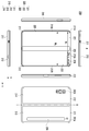
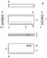
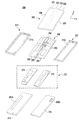
도 2a는 다양한 실시예에 따른 전자 장치의 펼침 상태를 도시한 도면이고, 도 2b는 도 2a의 전자 장치의 접힘 상태를 도시한 도면이고, 도 2c는 도 2a의 전자 장치의 분해 사시도이다.
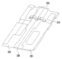
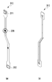
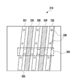
도 3a는 다양한 실시예에 따른 전자 장치에서 폴딩 축에 배치된 배선 부재를 도시한 도면이고, 도 3b는 배선 부재의 일면 및 타면을 도시한 도면이고, 도 3c는 배선 부재의 벤딩 영역에 대응하여 형성된 슬릿 구조를 도시한 도면이다.
도 4는 다양한 실시예에 따른, 벤딩 특성을 갖는 무선 주파수 전송 선로의 신호 전송 성능을 그래프로 도시한 도면이다.
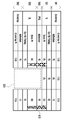
도 5a 내지 도 5b는 다양한 실시예에 따른, 마이크로 스트립(micro strip) 형태의 배선 부재의 구조를 도시한 도면이다.
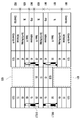
도 6a 내지 6b는 다양한 실시예에 따른, 스트립(strip) 형태의 배선 부재의 구조를 도시한 도면이다.
264 : 힌지 구조물 230 : 힌지 커버
310 : 배선 부재 333, 334 : 무선 주파수 전송 선로
330, 331, 332 : 접지 부재 336 : 비아(via)
340 : 슬릿 구조
Claims (20)
- 전자 장치에 있어서,
제 1 하우징;
상기 제 1 하우징이 제 1 면에 연결된 힌지부;
상기 제 1 면과 반대 방향인 상기 힌지부의 제 2 면에 연결된 제 2 하우징; 및
상기 제 1 하우징과 상기 제 2 하우징을 전기적으로 연결하는 배선 부재를 포함하고,
상기 배선 부재는 상기 힌지부에 기반하여 접히거나 펼쳐지고, 상기 접히거나 펼쳐지는 벤딩 영역의 적어도 일부에 대응하여 슬릿이 형성되는 전자 장치. - 제 1 항에 있어서,
상기 배선 부재는 벤딩이 가능한 연성 회로 기판(FPCB, flexible printed circuit board)을 기반으로 형성되는 전자 장치. - 제 1 항에 있어서,
상기 배선 부재는, 두 장의 기판을 기반으로 형성된 마이크로 스트립 형태의 배선 부재 및 세 장의 기판을 기반으로 형성된 스트립 형태의 배선 부재를 포함하는 전자 장치. - 제 3 항에 있어서,
상기 마이크로 스트립 형태의 배선 부재는,
제 1 기판 및 제 2 기판을 기반으로 형성되고,
상기 제 1 기판과 상기 제 2 기판이 적층되는 전자 장치. - 제 4 항에 있어서,
상기 마이크로 스트립 형태의 배선 부재는,
상기 제 1 기판에 대응하여 적어도 하나의 무선 주파수 전송 선로(RF line)가 형성되고, 상기 제 2 기판에 대응하여 슬릿이 형성되는 전자 장치. - 제 5 항에 있어서,
상기 슬릿은 상기 배선 부재가 접히거나 펼쳐지는 벤딩 영역에 대응하여 형성되는 전자 장치. - 제 5 항에 있어서,
상기 슬릿은 상기 제 1 기판과 상기 제 2 기판이 적층된 상태에서 상기 제 2 기판에 대응하는 추가적인 가공에 의해 형성되는 전자 장치. - 제 4 항에 있어서,
상기 마이크로 스트립 형태의 배선 부재는,
상기 벤딩 영역에 대응하여 상기 제 1 기판에 기반하는 적어도 하나의 무선 주파수 전송 선로가 형성되고, 상기 벤딩 영역에 대응하는 상기 배선 부재의 두께는 상기 제 1 기판에 대응하여 결정되는 전자 장치. - 제 4 항에 있어서,
상기 제 1 기판 및 상기 제 2 기판은 구리(CU) 기반의 도전성 부재(CU+Fill plating) 및 폴리이미드 필름(PI, polyimide film)을 기반으로 형성되는 전자 장치. - 제 3 항에 있어서,
상기 스트립 형태의 배선 부재는,
제 1 기판, 제 2 기판, 및 제 3 기판을 기반으로 형성되고,
상기 제 1 기판, 상기 제 2 기판, 및 상기 제 3 기판이 순서에 따라 적층되는 전자 장치. - 제 10 항에 있어서,
상기 스트립 형태의 배선 부재는,
상기 제 2 기판에 대응하여 적어도 하나의 무선 주파수 전송 선로(RF line)가 형성되고, 상기 제 1 기판에 대응하는 제 1 슬릿 및 상기 제 3 기판에 대응하는 제 2 슬릿이 형성되는 전자 장치. - 제 11 항에 있어서,
상기 제 1 슬릿 및 상기 제 2 슬릿은 상기 배선 부재가 접히거나 펼쳐지는 벤딩 영역에 대응하여 형성되는 전자 장치. - 제 11 항에 있어서,
상기 제 1 슬릿 및 상기 제 2 슬릿은 상기 제 1 기판, 상기 제 2 기판, 및 상기 제 3 기판이 적층된 상태에서 상기 제 1 기판에 대응하는 추가적인 가공에 의해 상기 제 1 슬릿이 형성되고, 상기 제 3 기판에 대응하는 추가적인 가공에 의해 상기 제 2 슬릿이 형성되는 전자 장치. - 제 10 항에 있어서,
상기 스트립 형태의 배선 부재는,
상기 벤딩 영역에 대응하여 상기 제 2 기판에 기반하는 적어도 하나의 무선 주파수 전송 선로가 형성되고, 상기 벤딩 영역에 대응하는 상기 배선 부재의 두께는 상기 제 2 기판에 대응하여 결정되는 전자 장치. - 제 10 항에 있어서,
상기 제 1 기판, 상기 제 2 기판 및 상기 제 3 기판은 구리(CU) 기반의 도전성 부재(CU+Fill plating) 및 폴리이미드 필름(PI, polyimide film)을 기반으로 형성되는 전자 장치. - 벤딩 가능한 배선 부재에 있어서,
제 1 기판; 및
상기 제 1 기판의 제 1 면에 적층된 제 2 기판;을 포함하고,
상기 제 1 기판을 기반으로 적어도 하나의 무선 주파수 전송 선로가 형성되고, 상기 배선 부재가 접히거나 펼쳐지는 벤딩 영역의 적어도 일부에 대응하여, 상기 제 2 기판에 제 1 슬릿이 형성되는 배선 부재. - 제 16 항에 있어서,
상기 제 1 기판의 상기 제 1 면과 반대 방향인 제 2 면에 적층된 제 3 기판;을 더 포함하고,
상기 벤딩 영역의 적어도 일부에 대응하여, 상기 제 3 기판에 제 2 슬릿이 형성되는 배선 부재. - 제 16 항 또는 제 17항에 있어서,
상기 벤딩 영역에 대응하는 상기 배선 부재의 두께는 상기 제 1 기판의 두께에 대응하여 결정되는 배선 부재. - 제 16 항 또는 제 17항에 있어서,
상기 제1 슬릿 및 상기 제 2 슬릿은 상기 제 1 기판, 상기 제 2 기판 및 상기 제 3 기판 중 적어도 일부가 적층된 상태에서 추가적인 가공에 의해 형성되는 배선 부재. - 제 17항에 있어서,
상기 제 1 기판, 상기 제 2 기판 및 상기 제 3 기판은 구리(CU) 기반의 도전성 부재(CU+Fill plating) 및 폴리이미드 필름(PI, polyimide film)을 기반으로 형성되는 배선 부재.
Priority Applications (3)
| Application Number | Priority Date | Filing Date | Title |
|---|---|---|---|
| KR1020180130103A KR102668961B1 (ko) | 2018-10-29 | 2018-10-29 | 벤딩 특성을 갖는 배선 부재 및 이를 포함하는 전자 장치 |
| US17/287,334 US11943888B2 (en) | 2018-10-29 | 2019-10-28 | Wiring member having bending property and electronic device comprising same |
| PCT/KR2019/014300 WO2020091354A1 (ko) | 2018-10-29 | 2019-10-28 | 벤딩 특성을 갖는 배선 부재 및 이를 포함하는 전자 장치 |
Applications Claiming Priority (1)
| Application Number | Priority Date | Filing Date | Title |
|---|---|---|---|
| KR1020180130103A KR102668961B1 (ko) | 2018-10-29 | 2018-10-29 | 벤딩 특성을 갖는 배선 부재 및 이를 포함하는 전자 장치 |
Publications (2)
| Publication Number | Publication Date |
|---|---|
| KR20200048238A true KR20200048238A (ko) | 2020-05-08 |
| KR102668961B1 KR102668961B1 (ko) | 2024-05-24 |
Family
ID=70461972
Family Applications (1)
| Application Number | Title | Priority Date | Filing Date |
|---|---|---|---|
| KR1020180130103A Active KR102668961B1 (ko) | 2018-10-29 | 2018-10-29 | 벤딩 특성을 갖는 배선 부재 및 이를 포함하는 전자 장치 |
Country Status (3)
| Country | Link |
|---|---|
| US (1) | US11943888B2 (ko) |
| KR (1) | KR102668961B1 (ko) |
| WO (1) | WO2020091354A1 (ko) |
Cited By (10)
| Publication number | Priority date | Publication date | Assignee | Title |
|---|---|---|---|---|
| WO2022019557A1 (ko) * | 2020-07-22 | 2022-01-27 | 삼성전자 주식회사 | 연성회로기판 및 이를 포함하는 전자 장치 |
| KR20220016591A (ko) * | 2020-08-03 | 2022-02-10 | 삼성전자주식회사 | 가요성 인쇄회로 기판을 포함하는 전자 장치 |
| WO2022169084A1 (ko) * | 2021-02-04 | 2022-08-11 | 삼성전자 주식회사 | 연성회로기판 및 이를 포함하는 폴더블 전자 장치 |
| WO2022203431A1 (ko) * | 2021-03-24 | 2022-09-29 | 삼성전자 주식회사 | 플렉서블 접속 부재 및 그를 포함하는 전자 장치 |
| WO2023090629A1 (ko) * | 2021-11-22 | 2023-05-25 | 삼성전자주식회사 | 전자 장치 |
| US11775015B2 (en) | 2020-08-03 | 2023-10-03 | Samsung Electronics Co., Ltd. | Electronic device including flexible printed circuit board |
| WO2024071732A1 (ko) * | 2022-09-26 | 2024-04-04 | 삼성전자 주식회사 | 플렉서블 회로 기판 및 이를 포함하는 전자 장치 |
| EP4258827A4 (en) * | 2021-01-06 | 2024-08-21 | Samsung Electronics Co., Ltd. | PRINTED CIRCUIT BOARD AND ELECTRONIC DEVICE COMPRISING SAME |
| WO2025018566A1 (ko) * | 2023-07-17 | 2025-01-23 | 삼성전자 주식회사 | 가요성 인쇄회로 기판을 포함하는 전자 장치 |
| US12537890B2 (en) | 2021-05-07 | 2026-01-27 | Samsung Electronics Co., Ltd. | Flexible circuit board and foldable electronic device comprising same |
Families Citing this family (2)
| Publication number | Priority date | Publication date | Assignee | Title |
|---|---|---|---|---|
| JP7226110B2 (ja) * | 2019-05-31 | 2023-02-21 | 株式会社オートネットワーク技術研究所 | 配線部材 |
| KR102738447B1 (ko) | 2020-02-10 | 2024-12-05 | 삼성전자주식회사 | 폴더블 전자 장치 |
Citations (2)
| Publication number | Priority date | Publication date | Assignee | Title |
|---|---|---|---|---|
| JP2008065728A (ja) * | 2006-09-11 | 2008-03-21 | Hitachi Displays Ltd | 情報処理装置 |
| KR20160046605A (ko) * | 2014-10-21 | 2016-04-29 | 삼성전자주식회사 | 접철식 전자 장치 |
Family Cites Families (11)
| Publication number | Priority date | Publication date | Assignee | Title |
|---|---|---|---|---|
| JPH07122856A (ja) | 1993-10-20 | 1995-05-12 | Sumitomo Electric Ind Ltd | フレクスリジッド多層板とその製法 |
| JP3703067B2 (ja) | 1999-05-20 | 2005-10-05 | シャープ株式会社 | フレックスリジット多層配線板の製造方法 |
| US20080045093A1 (en) * | 2003-10-31 | 2008-02-21 | Richard Terrence Tamba | De-Coupling Clutch, Particularly for Marine Use |
| JP2005251958A (ja) | 2004-03-04 | 2005-09-15 | Fujikura Ltd | フレキシブルプリント配線基板及びフラットケーブル |
| JP5584085B2 (ja) * | 2010-10-14 | 2014-09-03 | パナソニック株式会社 | フレキシブル基板、および電子機器 |
| JP5584086B2 (ja) * | 2010-10-14 | 2014-09-03 | パナソニック株式会社 | 電子機器 |
| JP2013157490A (ja) | 2012-01-31 | 2013-08-15 | Jvc Kenwood Corp | 両面フレキシブルプリント基板及び両面フレキシブルプリント基板用コネクタ |
| KR102364151B1 (ko) | 2015-03-18 | 2022-02-18 | 주식회사 기가레인 | 연성회로기판 |
| KR102366299B1 (ko) | 2015-08-31 | 2022-02-21 | 엘지디스플레이 주식회사 | 플렉서블 디스플레이용 지지 프레임 및 이를 포함하는 플렉서블 디스플레이 장치 |
| JP6634518B2 (ja) * | 2016-05-31 | 2020-01-22 | Gvido Music株式会社 | 電子機器用ヒンジ及び電子機器 |
| KR102364129B1 (ko) * | 2017-09-28 | 2022-02-16 | 엘지디스플레이 주식회사 | 연성 디스플레이 장치 |
-
2018
- 2018-10-29 KR KR1020180130103A patent/KR102668961B1/ko active Active
-
2019
- 2019-10-28 US US17/287,334 patent/US11943888B2/en active Active
- 2019-10-28 WO PCT/KR2019/014300 patent/WO2020091354A1/ko not_active Ceased
Patent Citations (2)
| Publication number | Priority date | Publication date | Assignee | Title |
|---|---|---|---|---|
| JP2008065728A (ja) * | 2006-09-11 | 2008-03-21 | Hitachi Displays Ltd | 情報処理装置 |
| KR20160046605A (ko) * | 2014-10-21 | 2016-04-29 | 삼성전자주식회사 | 접철식 전자 장치 |
Cited By (18)
| Publication number | Priority date | Publication date | Assignee | Title |
|---|---|---|---|---|
| US12273992B2 (en) | 2020-07-22 | 2025-04-08 | Samsung Electronics Co., Ltd. | Flexible printed circuit board and electronic device including the same |
| WO2022019557A1 (ko) * | 2020-07-22 | 2022-01-27 | 삼성전자 주식회사 | 연성회로기판 및 이를 포함하는 전자 장치 |
| KR20220016591A (ko) * | 2020-08-03 | 2022-02-10 | 삼성전자주식회사 | 가요성 인쇄회로 기판을 포함하는 전자 장치 |
| WO2022030775A1 (ko) * | 2020-08-03 | 2022-02-10 | 삼성전자 주식회사 | 가요성 인쇄회로 기판을 포함하는 전자 장치 |
| US12181924B2 (en) | 2020-08-03 | 2024-12-31 | Samsung Electronics Co., Ltd. | Electronic device including flexible printed circuit board |
| US11775015B2 (en) | 2020-08-03 | 2023-10-03 | Samsung Electronics Co., Ltd. | Electronic device including flexible printed circuit board |
| US12563660B2 (en) | 2021-01-06 | 2026-02-24 | Samsung Electronics Co., Ltd. | Circuit board and electronic device comprising same |
| EP4258827A4 (en) * | 2021-01-06 | 2024-08-21 | Samsung Electronics Co., Ltd. | PRINTED CIRCUIT BOARD AND ELECTRONIC DEVICE COMPRISING SAME |
| WO2022169084A1 (ko) * | 2021-02-04 | 2022-08-11 | 삼성전자 주식회사 | 연성회로기판 및 이를 포함하는 폴더블 전자 장치 |
| EP4274392A4 (en) * | 2021-02-04 | 2024-06-19 | Samsung Electronics Co., Ltd. | Flexible circuit board and foldable electronic device comprising same |
| JP2024506284A (ja) * | 2021-02-04 | 2024-02-13 | サムスン エレクトロニクス カンパニー リミテッド | フレキシブル回路基板及びそれを含むフォルダブル電子装置 |
| AU2021425425B2 (en) * | 2021-02-04 | 2024-10-10 | Samsung Electronics Co., Ltd. | Flexible circuit board and foldable electronic device comprising same |
| JP7836320B2 (ja) | 2021-02-04 | 2026-03-26 | サムスン エレクトロニクス カンパニー リミテッド | フレキシブル回路基板及びそれを含むフォルダブル電子装置 |
| WO2022203431A1 (ko) * | 2021-03-24 | 2022-09-29 | 삼성전자 주식회사 | 플렉서블 접속 부재 및 그를 포함하는 전자 장치 |
| US12537890B2 (en) | 2021-05-07 | 2026-01-27 | Samsung Electronics Co., Ltd. | Flexible circuit board and foldable electronic device comprising same |
| WO2023090629A1 (ko) * | 2021-11-22 | 2023-05-25 | 삼성전자주식회사 | 전자 장치 |
| WO2024071732A1 (ko) * | 2022-09-26 | 2024-04-04 | 삼성전자 주식회사 | 플렉서블 회로 기판 및 이를 포함하는 전자 장치 |
| WO2025018566A1 (ko) * | 2023-07-17 | 2025-01-23 | 삼성전자 주식회사 | 가요성 인쇄회로 기판을 포함하는 전자 장치 |
Also Published As
| Publication number | Publication date |
|---|---|
| WO2020091354A1 (ko) | 2020-05-07 |
| US20210360814A1 (en) | 2021-11-18 |
| KR102668961B1 (ko) | 2024-05-24 |
| US11943888B2 (en) | 2024-03-26 |
Similar Documents
| Publication | Publication Date | Title |
|---|---|---|
| KR102668961B1 (ko) | 벤딩 특성을 갖는 배선 부재 및 이를 포함하는 전자 장치 | |
| KR102575550B1 (ko) | 굴곡부를 포함하는 인쇄 회로 기판 및 이를 포함하는 전자 장치 | |
| KR102800454B1 (ko) | 안테나 및 그것을 포함하는 전자 장치 | |
| US11700693B2 (en) | Foldable electronic device including flexible printed circuit board | |
| US11294429B2 (en) | Flexible display device including heat dissipation structure | |
| US10833397B2 (en) | Foldable device comprising antenna | |
| KR102746762B1 (ko) | 안테나를 포함하는 폴더블 전자 장치 | |
| US11204624B2 (en) | Foldable electronic device including magnets | |
| US10594023B2 (en) | Electronic device including conductive member electrically coupled to opening of bracket for adjusting resonance generated from the opening | |
| KR102761558B1 (ko) | 접이식 전자 장치 | |
| KR20200101116A (ko) | 통합된 접지 구조를 포함하는 폴더블 전자 장치 | |
| US11758032B2 (en) | Electronic device comprising haptic actuator | |
| KR20210041985A (ko) | 복수 개의 배터리를 포함하는 전자 장치 | |
| KR20260005701A (ko) | 방열 구조를 포함하는 전자 장치 | |
| KR20250057585A (ko) | 인쇄 회로 기판을 지지하기 위한 구조를 포함하는 전자 장치 |
Legal Events
| Date | Code | Title | Description |
|---|---|---|---|
| PA0109 | Patent application |
Patent event code: PA01091R01D Comment text: Patent Application Patent event date: 20181029 |
|
| PG1501 | Laying open of application | ||
| A201 | Request for examination | ||
| PA0201 | Request for examination |
Patent event code: PA02012R01D Patent event date: 20211029 Comment text: Request for Examination of Application Patent event code: PA02011R01I Patent event date: 20181029 Comment text: Patent Application |
|
| E902 | Notification of reason for refusal | ||
| PE0902 | Notice of grounds for rejection |
Comment text: Notification of reason for refusal Patent event date: 20231020 Patent event code: PE09021S01D |
|
| E701 | Decision to grant or registration of patent right | ||
| PE0701 | Decision of registration |
Patent event code: PE07011S01D Comment text: Decision to Grant Registration Patent event date: 20240321 |
|
| GRNT | Written decision to grant | ||
| PR0701 | Registration of establishment |
Comment text: Registration of Establishment Patent event date: 20240521 Patent event code: PR07011E01D |
|
| PR1002 | Payment of registration fee |
Payment date: 20240522 End annual number: 3 Start annual number: 1 |
|
| PG1601 | Publication of registration |