KR20200048978A - 데이터 저장 장치 및 그것의 동작 방법 - Google Patents
데이터 저장 장치 및 그것의 동작 방법 Download PDFInfo
- Publication number
- KR20200048978A KR20200048978A KR1020180131695A KR20180131695A KR20200048978A KR 20200048978 A KR20200048978 A KR 20200048978A KR 1020180131695 A KR1020180131695 A KR 1020180131695A KR 20180131695 A KR20180131695 A KR 20180131695A KR 20200048978 A KR20200048978 A KR 20200048978A
- Authority
- KR
- South Korea
- Prior art keywords
- block
- memory
- memory block
- super
- replacement
- Prior art date
- Legal status (The legal status is an assumption and is not a legal conclusion. Google has not performed a legal analysis and makes no representation as to the accuracy of the status listed.)
- Granted
Links
Images




Classifications
-
- G—PHYSICS
- G06—COMPUTING OR CALCULATING; COUNTING
- G06F—ELECTRIC DIGITAL DATA PROCESSING
- G06F3/00—Input arrangements for transferring data to be processed into a form capable of being handled by the computer; Output arrangements for transferring data from processing unit to output unit, e.g. interface arrangements
- G06F3/06—Digital input from, or digital output to, record carriers, e.g. RAID, emulated record carriers or networked record carriers
- G06F3/0601—Interfaces specially adapted for storage systems
- G06F3/0628—Interfaces specially adapted for storage systems making use of a particular technique
- G06F3/0655—Vertical data movement, i.e. input-output transfer; data movement between one or more hosts and one or more storage devices
- G06F3/0658—Controller construction arrangements
-
- G—PHYSICS
- G06—COMPUTING OR CALCULATING; COUNTING
- G06F—ELECTRIC DIGITAL DATA PROCESSING
- G06F12/00—Accessing, addressing or allocating within memory systems or architectures
- G06F12/02—Addressing or allocation; Relocation
- G06F12/0223—User address space allocation, e.g. contiguous or non contiguous base addressing
- G06F12/023—Free address space management
- G06F12/0238—Memory management in non-volatile memory, e.g. resistive RAM or ferroelectric memory
- G06F12/0246—Memory management in non-volatile memory, e.g. resistive RAM or ferroelectric memory in block erasable memory, e.g. flash memory
-
- G—PHYSICS
- G06—COMPUTING OR CALCULATING; COUNTING
- G06F—ELECTRIC DIGITAL DATA PROCESSING
- G06F13/00—Interconnection of, or transfer of information or other signals between, memories, input/output devices or central processing units
- G06F13/14—Handling requests for interconnection or transfer
- G06F13/16—Handling requests for interconnection or transfer for access to memory bus
- G06F13/1668—Details of memory controller
-
- G—PHYSICS
- G06—COMPUTING OR CALCULATING; COUNTING
- G06F—ELECTRIC DIGITAL DATA PROCESSING
- G06F11/00—Error detection; Error correction; Monitoring
- G06F11/07—Responding to the occurrence of a fault, e.g. fault tolerance
- G06F11/0703—Error or fault processing not based on redundancy, i.e. by taking additional measures to deal with the error or fault not making use of redundancy in operation, in hardware, or in data representation
- G06F11/0706—Error or fault processing not based on redundancy, i.e. by taking additional measures to deal with the error or fault not making use of redundancy in operation, in hardware, or in data representation the processing taking place on a specific hardware platform or in a specific software environment
- G06F11/073—Error or fault processing not based on redundancy, i.e. by taking additional measures to deal with the error or fault not making use of redundancy in operation, in hardware, or in data representation the processing taking place on a specific hardware platform or in a specific software environment in a memory management context, e.g. virtual memory or cache management
-
- G—PHYSICS
- G06—COMPUTING OR CALCULATING; COUNTING
- G06F—ELECTRIC DIGITAL DATA PROCESSING
- G06F11/00—Error detection; Error correction; Monitoring
- G06F11/07—Responding to the occurrence of a fault, e.g. fault tolerance
- G06F11/08—Error detection or correction by redundancy in data representation, e.g. by using checking codes
- G06F11/10—Adding special bits or symbols to the coded information, e.g. parity check, casting out 9's or 11's
- G06F11/1008—Adding special bits or symbols to the coded information, e.g. parity check, casting out 9's or 11's in individual solid state devices
- G06F11/1012—Adding special bits or symbols to the coded information, e.g. parity check, casting out 9's or 11's in individual solid state devices using codes or arrangements adapted for a specific type of error
-
- G—PHYSICS
- G06—COMPUTING OR CALCULATING; COUNTING
- G06F—ELECTRIC DIGITAL DATA PROCESSING
- G06F11/00—Error detection; Error correction; Monitoring
- G06F11/07—Responding to the occurrence of a fault, e.g. fault tolerance
- G06F11/08—Error detection or correction by redundancy in data representation, e.g. by using checking codes
- G06F11/10—Adding special bits or symbols to the coded information, e.g. parity check, casting out 9's or 11's
- G06F11/1008—Adding special bits or symbols to the coded information, e.g. parity check, casting out 9's or 11's in individual solid state devices
- G06F11/1048—Adding special bits or symbols to the coded information, e.g. parity check, casting out 9's or 11's in individual solid state devices using arrangements adapted for a specific error detection or correction feature
-
- G—PHYSICS
- G06—COMPUTING OR CALCULATING; COUNTING
- G06F—ELECTRIC DIGITAL DATA PROCESSING
- G06F11/00—Error detection; Error correction; Monitoring
- G06F11/07—Responding to the occurrence of a fault, e.g. fault tolerance
- G06F11/16—Error detection or correction of the data by redundancy in hardware
- G06F11/1658—Data re-synchronization of a redundant component, or initial sync of replacement, additional or spare unit
-
- G—PHYSICS
- G06—COMPUTING OR CALCULATING; COUNTING
- G06F—ELECTRIC DIGITAL DATA PROCESSING
- G06F11/00—Error detection; Error correction; Monitoring
- G06F11/07—Responding to the occurrence of a fault, e.g. fault tolerance
- G06F11/16—Error detection or correction of the data by redundancy in hardware
- G06F11/20—Error detection or correction of the data by redundancy in hardware using active fault-masking, e.g. by switching out faulty elements or by switching in spare elements
- G06F11/2053—Error detection or correction of the data by redundancy in hardware using active fault-masking, e.g. by switching out faulty elements or by switching in spare elements where persistent mass storage functionality or persistent mass storage control functionality is redundant
- G06F11/2094—Redundant storage or storage space
-
- G—PHYSICS
- G06—COMPUTING OR CALCULATING; COUNTING
- G06F—ELECTRIC DIGITAL DATA PROCESSING
- G06F12/00—Accessing, addressing or allocating within memory systems or architectures
- G06F12/02—Addressing or allocation; Relocation
- G06F12/06—Addressing a physical block of locations, e.g. base addressing, module addressing, memory dedication
- G06F12/0607—Interleaved addressing
-
- G—PHYSICS
- G06—COMPUTING OR CALCULATING; COUNTING
- G06F—ELECTRIC DIGITAL DATA PROCESSING
- G06F3/00—Input arrangements for transferring data to be processed into a form capable of being handled by the computer; Output arrangements for transferring data from processing unit to output unit, e.g. interface arrangements
- G06F3/06—Digital input from, or digital output to, record carriers, e.g. RAID, emulated record carriers or networked record carriers
- G06F3/0601—Interfaces specially adapted for storage systems
- G06F3/0602—Interfaces specially adapted for storage systems specifically adapted to achieve a particular effect
- G06F3/061—Improving I/O performance
-
- G—PHYSICS
- G06—COMPUTING OR CALCULATING; COUNTING
- G06F—ELECTRIC DIGITAL DATA PROCESSING
- G06F3/00—Input arrangements for transferring data to be processed into a form capable of being handled by the computer; Output arrangements for transferring data from processing unit to output unit, e.g. interface arrangements
- G06F3/06—Digital input from, or digital output to, record carriers, e.g. RAID, emulated record carriers or networked record carriers
- G06F3/0601—Interfaces specially adapted for storage systems
- G06F3/0628—Interfaces specially adapted for storage systems making use of a particular technique
- G06F3/0629—Configuration or reconfiguration of storage systems
-
- G—PHYSICS
- G06—COMPUTING OR CALCULATING; COUNTING
- G06F—ELECTRIC DIGITAL DATA PROCESSING
- G06F3/00—Input arrangements for transferring data to be processed into a form capable of being handled by the computer; Output arrangements for transferring data from processing unit to output unit, e.g. interface arrangements
- G06F3/06—Digital input from, or digital output to, record carriers, e.g. RAID, emulated record carriers or networked record carriers
- G06F3/0601—Interfaces specially adapted for storage systems
- G06F3/0628—Interfaces specially adapted for storage systems making use of a particular technique
- G06F3/0638—Organizing or formatting or addressing of data
- G06F3/064—Management of blocks
-
- G—PHYSICS
- G06—COMPUTING OR CALCULATING; COUNTING
- G06F—ELECTRIC DIGITAL DATA PROCESSING
- G06F3/00—Input arrangements for transferring data to be processed into a form capable of being handled by the computer; Output arrangements for transferring data from processing unit to output unit, e.g. interface arrangements
- G06F3/06—Digital input from, or digital output to, record carriers, e.g. RAID, emulated record carriers or networked record carriers
- G06F3/0601—Interfaces specially adapted for storage systems
- G06F3/0628—Interfaces specially adapted for storage systems making use of a particular technique
- G06F3/0646—Horizontal data movement in storage systems, i.e. moving data in between storage devices or systems
- G06F3/0647—Migration mechanisms
-
- G—PHYSICS
- G06—COMPUTING OR CALCULATING; COUNTING
- G06F—ELECTRIC DIGITAL DATA PROCESSING
- G06F3/00—Input arrangements for transferring data to be processed into a form capable of being handled by the computer; Output arrangements for transferring data from processing unit to output unit, e.g. interface arrangements
- G06F3/06—Digital input from, or digital output to, record carriers, e.g. RAID, emulated record carriers or networked record carriers
- G06F3/0601—Interfaces specially adapted for storage systems
- G06F3/0628—Interfaces specially adapted for storage systems making use of a particular technique
- G06F3/0655—Vertical data movement, i.e. input-output transfer; data movement between one or more hosts and one or more storage devices
- G06F3/0656—Data buffering arrangements
-
- G—PHYSICS
- G06—COMPUTING OR CALCULATING; COUNTING
- G06F—ELECTRIC DIGITAL DATA PROCESSING
- G06F3/00—Input arrangements for transferring data to be processed into a form capable of being handled by the computer; Output arrangements for transferring data from processing unit to output unit, e.g. interface arrangements
- G06F3/06—Digital input from, or digital output to, record carriers, e.g. RAID, emulated record carriers or networked record carriers
- G06F3/0601—Interfaces specially adapted for storage systems
- G06F3/0668—Interfaces specially adapted for storage systems adopting a particular infrastructure
- G06F3/0671—In-line storage system
- G06F3/0683—Plurality of storage devices
- G06F3/0688—Non-volatile semiconductor memory arrays
-
- G—PHYSICS
- G11—INFORMATION STORAGE
- G11C—STATIC STORES
- G11C29/00—Checking stores for correct operation ; Subsequent repair; Testing stores during standby or offline operation
- G11C29/04—Detection or location of defective memory elements, e.g. cell constructio details, timing of test signals
- G11C29/08—Functional testing, e.g. testing during refresh, power-on self testing [POST] or distributed testing
- G11C29/12—Built-in arrangements for testing, e.g. built-in self testing [BIST] or interconnection details
- G11C29/38—Response verification devices
- G11C29/42—Response verification devices using error correcting codes [ECC] or parity check
-
- G—PHYSICS
- G11—INFORMATION STORAGE
- G11C—STATIC STORES
- G11C29/00—Checking stores for correct operation ; Subsequent repair; Testing stores during standby or offline operation
- G11C29/70—Masking faults in memories by using spares or by reconfiguring
- G11C29/88—Masking faults in memories by using spares or by reconfiguring with partially good memories
- G11C29/886—Masking faults in memories by using spares or by reconfiguring with partially good memories combining plural defective memory devices to provide a contiguous address range, e.g. one device supplies working blocks to replace defective blocks in another device
-
- G—PHYSICS
- G06—COMPUTING OR CALCULATING; COUNTING
- G06F—ELECTRIC DIGITAL DATA PROCESSING
- G06F2212/00—Indexing scheme relating to accessing, addressing or allocation within memory systems or architectures
- G06F2212/72—Details relating to flash memory management
- G06F2212/7203—Temporary buffering, e.g. using volatile buffer or dedicated buffer blocks
Landscapes
- Engineering & Computer Science (AREA)
- Theoretical Computer Science (AREA)
- Physics & Mathematics (AREA)
- General Engineering & Computer Science (AREA)
- General Physics & Mathematics (AREA)
- Human Computer Interaction (AREA)
- Quality & Reliability (AREA)
- Techniques For Improving Reliability Of Storages (AREA)
Abstract
Description
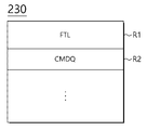
도 2는 도 1의 메모리의 구성을 나타낸 도면.
도 3은 본 발명의 일 실시예에 따른 불휘발성 메모리 장치에 포함된 데이터 저장 영역을 설명하기 위한 도면.
도 4는 도 1에 도시된 불휘발성 메모리 장치의 일 예를 설명하기 위한 도면.
도 5는 본 발명의 일 실시예에 따른 도 2에 도시된 FTL의 블록도.
도 6은 본 발명의 일 실시예에 따른 데이터 저장 장치 동작 방법의 흐름도.
도 7 내지 도 9는 본 발명의 일 실시예에 따른 대체 블록을 설명하기 위한 도면.
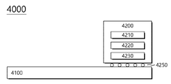
도 10은 본 발명의 실시 예에 따른 솔리드 스테이트 드라이브(SSD)를 포함하는 데이터 처리 시스템을 예시적으로 나타낸 도면.
도 11은 도 10의 컨트롤러의 구성을 예시적으로 나타낸 도면.
도 12는 본 발명의 실시 예에 따른 데이터 저장 장치를 포함하는 데이터 처리 시스템을 예시적으로 나타낸 도면.
도 13은 본 발명의 실시 예에 따른 데이터 저장 장치를 포함하는 데이터 처리 시스템을 예시적으로 나타낸 도면.
도 14는 본 발명의 실시 예에 따른 데이터 저장 장치를 포함하는 네트워크 시스템을 예시적으로 나타낸 도면.
도 15는 본 발명의 실시 예에 따른 데이터 저장 장치에 포함된 불휘발성 메모리 장치를 예시적으로 나타낸 블록도.
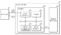
200: 컨트롤러 210: 호스트 인터페이스
220: 프로세서 230: 메모리
240: 메모리 인터페이스
Claims (17)
- 복수의 플레인을 포함하되 상기 플레인 각각은 적어도 2 이상의 메모리 블록을 포함하는 메모리 장치와, 상기 메모리 장치의 동작을 제어하는 컨트롤러를 포함하되,
상기 컨트롤러는,
상기 복수의 메모리 블록 중 웨이 인터리빙이 가능한 적어도 2이상의 메모리 블록을 포함하는 슈퍼 블록인 제1 슈퍼 블록을 생성하고,
상기 제1 슈퍼 블록에 포함된 메모리 블록에 대한 배드 블록 여부를 판단하여,
배드 블록으로 판단된 메모리 블록인 제1 메모리 블록을 대체하기 위한 대체 블록을 검색하며,
웨이 인터리빙이 가능한 대체 블록이 존재하지 않으면, 웨이 인터리빙이 불가한 대체 블록인 제2 메모리 블록으로 상기 제1 메모리 블록을 대체한 슈퍼 블록인 제2 슈퍼 블록을 생성하고,
상기 제2 슈퍼 블록이 생성된 이후 가용하게 된, 상기 제2 메모리 블록을 대체하기 위한 웨이 인터리빙 가능한 대체 블록인 제3 메모리 블록을 검색하며,
상기 제3 메모리 블록으로 상기 제2 메모리 블록을 대체한 슈퍼 블록인 제3 슈퍼 블록을 생성하는 데이터 저장 장치. - 제 1 항에 있어서,
상기 컨트롤러는,
각각 상이한 플레인에 포함된 적어도 2 이상의 메모리 블록을 기반으로 상기 제1 슈퍼 블록을 생성하는 것을 특징으로 하는 데이터 저장 장치. - 제 1 항에 있어서,
상기 컨트롤러는,
상기 제1 슈퍼 블록에 포함된 메모리 블록 중 쓰기 동작 페일이 발생하는 메모리 블록을 배드 블록으로 판단하는 것을 특징으로 하는 데이터 저장 장치. - 제 1 항에 있어서,
상기 메모리 장치는,
각각 상기 메모리 장치에 포함된 메모리 블록 중 적어도 2이상의 메모리 블록을 포함하는 제1 대체 메모리 블록 그룹 및 제2 대체 메모리 블록 그룹을 포함하되,
상기 컨트롤러는,
상기 제1 대체 메모리 블록 그룹에 포함된 메모리 블록을 검색하는 것을 특징으로 하는 데이터 저장 장치. - 제 4 항에 있어서,
상기 컨트롤러는,
상기 제1 대체 메모리 블록 그룹에 포함된 메모리 블록 중 가용한 메모리 블록이 없는 경우, 상기 제2 대체 메모리 블록 그룹에 포함된 메모리 블록을 검색하는 것을 특징으로 하는 데이터 저장 장치. - 제 1 항에 있어서,
상기 컨트롤러는,
상기 웨이 인터리빙이 가능한 대체 블록인 제4 메모리 블록이 존재하면, 상기 제4 메모리 블록으로 상기 제1 메모리 블록을 대체한 슈퍼 블록인 제4 슈퍼 블록을 생성하는 것을 특징으로 하는 데이터 저장 장치. - 제 1 항에 있어서,
상기 웨이 인터리빙이 가능한 대체 블록은 상기 제2 메모리 블록과 동일한 플레인에 포함된 메모리 블록인 것을 특징으로 하는 데이터 저장 장치. - 제 4 항에 있어서,
상기 컨트롤러는,
상기 제2 메모리 블록이 상기 제1 대체 메모리 블록 그룹에 포함되고, 상기 제2 슈퍼 블록이 생성된 이후 상기 제1 대체 메모리 블록 그룹에 가용한 메모리 블록이 존재하지 않는 경우,
상기 제2 대체 메모리 블록 그룹에 포함된 메모리 블록 중 상기 제1 메모리 블록과 동일한 플레인에 포함된 메모리 블록을 검색하는 것을 특징으로 하는 데이터 저장 장치. - 복수의 메모리 블록을 포함하는 메모리 장치와, 상기 메모리 장치의 동작을 제어하는 컨트롤러를 포함하는 데이터 저장 장치의 동작 방법에 있어서,
상기 복수의 메모리 블록 중 웨이 인터리빙이 가능한 적어도 2이상의 메모리 블록을 포함하는 슈퍼 블록인 제1 슈퍼 블록을 생성하는 단계;
상기 제1 슈퍼 블록에 포함된 메모리 블록에 대한 배드 블록 여부를 판단하는 단계;
배드 블록으로 판단된 메모리 블록인 제1 메모리 블록을 대체하기 위한 대체 블록을 검색하는 단계;
웨이 인터리빙이 가능한 대체 블록이 존재하지 않으면, 웨이 인터리빙이 불가한 대체 블록인 제2 메모리 블록으로 상기 제1 메모리 블록을 대체한 슈퍼 블록인 제2 슈퍼 블록을 생성하는 단계;
상기 제2 슈퍼 블록이 생성된 이후 가용하게 된, 상기 제2 메모리 블록을 대체하기 위한 웨이 인터리빙 가능한 대체 블록인 제3 메모리 블록을 검색하는 단계; 및
상기 제3 메모리 블록으로 상기 제2 메모리 블록을 대체한 슈퍼 블록인 제3 슈퍼 블록을 생성하는 단계
를 포함하는 데이터 저장 장치 동작 방법. - 제 9 항에 있어서,
상기 메모리 장치는,
각각 적어도 하나의 메모리 블록을 포함하는 복수의 플레인을 포함하되,
상기 제1 슈퍼 블록을 생성하는 단계는,
각각 상이한 플레인에 포함된 적어도 2 이상의 메모리 블록을 기반으로 상기 제1 슈퍼 블록을 생성하는 것을 특징으로 하는 데이터 저장 장치 동작 방법. - 제 9 항에 있어서,
상기 배드 블록 여부를 판단하는 단계는,
상기 제1 슈퍼 블록에 포함된 메모리 블록 중 쓰기 동작 페일이 발생하는 메모리 블록을 배드 블록으로 판단하는 것을 특징으로 하는 데이터 저장 장치 동작 방법. - 제 9 항에 있어서,
상기 메모리 장치는,
각각 상기 복수의 메모리 블록 중 적어도 2이상의 메모리 블록을 포함하는 제1 대체 메모리 블록 그룹 및 제2 대체 메모리 블록 그룹을 포함하되,
상기 대체 블록을 검색하는 단계는,
상기 제1 대체 메모리 블록 그룹에 포함된 메모리 블록을 검색하는 것을 특징으로 하는 데이터 저장 장치 동작 방법. - 제 12 항에 있어서,
상기 대체 블록을 검색하는 단계는,
상기 제1 대체 메모리 블록 그룹에 포함된 메모리 블록 중 가용한 메모리 블록이 없는 경우, 상기 제2 대체 메모리 블록 그룹에 포함된 메모리 블록을 검색하는 것을 특징으로 하는 데이터 저장 장치 동작 방법. - 제 9 항에 있어서,
상기 제2 슈퍼 블록을 생성하는 단계는,
상기 웨이 인터리빙이 가능한 대체 블록인 제4 메모리 블록이 존재하면, 상기 제4 메모리 블록으로 상기 제1 메모리 블록을 대체한 슈퍼 블록인 제4 슈퍼 블록을 생성하는 것을 특징으로 하는 데이터 저장 장치 동작 방법. - 제 9 항에 있어서,
상기 웨이 인터리빙이 가능한 대체 블록은 상기 제2 메모리 블록과 동일한 플레인에 포함된 메모리 블록인 것을 특징으로 하는 데이터 저장 장치 동작 방법. - 제 12 항에 있어서,
상기 제3 메모리 블록을 검색하는 단계는,
상기 제2 메모리 블록이 상기 제1 대체 메모리 블록 그룹에 포함되고, 상기 제2 슈퍼 블록이 생성된 이후 상기 제1 대체 메모리 블록 그룹에 가용한 메모리 블록이 존재하지 않는 경우,
상기 제2 대체 메모리 블록 그룹에 포함된 메모리 블록 중 상기 제1 메모리 블록과 동일한 플레인에 포함된 메모리 블록을 검색하는 것을 특징으로 하는 데이터 저장 장치 동작 방법. - 제 9 항에 있어서,
상기 각 단계 중 적어도 하나는 백 그라운드 동작으로 수행되는 것을 특징으로 하는 데이터 저장 장치 동작 방법.
Priority Applications (4)
| Application Number | Priority Date | Filing Date | Title |
|---|---|---|---|
| KR1020180131695A KR102592803B1 (ko) | 2018-10-31 | 2018-10-31 | 데이터 저장 장치 및 그것의 동작 방법 |
| US16/588,316 US11275678B2 (en) | 2018-10-31 | 2019-09-30 | Data storage device with spare blocks for replacing bad block in super block and operating method thereof |
| CN201910983437.4A CN111124273B (zh) | 2018-10-31 | 2019-10-16 | 数据存储装置及数据存储装置的操作方法 |
| US17/694,033 US20220197788A1 (en) | 2018-10-31 | 2022-03-14 | Data storage device with spare blocks for replacing bad block in super block and operating method thereof |
Applications Claiming Priority (1)
| Application Number | Priority Date | Filing Date | Title |
|---|---|---|---|
| KR1020180131695A KR102592803B1 (ko) | 2018-10-31 | 2018-10-31 | 데이터 저장 장치 및 그것의 동작 방법 |
Publications (2)
| Publication Number | Publication Date |
|---|---|
| KR20200048978A true KR20200048978A (ko) | 2020-05-08 |
| KR102592803B1 KR102592803B1 (ko) | 2023-10-24 |
Family
ID=70327163
Family Applications (1)
| Application Number | Title | Priority Date | Filing Date |
|---|---|---|---|
| KR1020180131695A Active KR102592803B1 (ko) | 2018-10-31 | 2018-10-31 | 데이터 저장 장치 및 그것의 동작 방법 |
Country Status (3)
| Country | Link |
|---|---|
| US (2) | US11275678B2 (ko) |
| KR (1) | KR102592803B1 (ko) |
| CN (1) | CN111124273B (ko) |
Cited By (2)
| Publication number | Priority date | Publication date | Assignee | Title |
|---|---|---|---|---|
| CN113220508A (zh) * | 2021-05-08 | 2021-08-06 | 联芸科技(杭州)有限公司 | 存储器块的管理方法、存储器的写操作方法以及存储器 |
| US11914891B2 (en) | 2021-10-07 | 2024-02-27 | SK Hynix Inc. | Storage device and operating method thereof |
Families Citing this family (9)
| Publication number | Priority date | Publication date | Assignee | Title |
|---|---|---|---|---|
| KR102517681B1 (ko) * | 2018-06-05 | 2023-04-05 | 에스케이하이닉스 주식회사 | 메모리 시스템 및 그것의 동작방법 |
| JP2023044518A (ja) | 2021-09-17 | 2023-03-30 | キオクシア株式会社 | メモリシステムおよび方法 |
| US11687263B2 (en) * | 2021-12-01 | 2023-06-27 | Western Digital Technologies, Inc. | Full die recovery in ZNS SSD |
| US11842062B2 (en) * | 2022-02-09 | 2023-12-12 | Western Digital Technologies, Inc. | Method of handling irregular MetaBlock wear leveling and UGSD boot time improvement |
| US12430037B2 (en) * | 2023-02-10 | 2025-09-30 | SanDisk Technologies, Inc. | Illusory free data storage space in data storage devices |
| CN119207523B (zh) * | 2023-06-26 | 2026-03-20 | 珠海横琴芯存半导体有限公司 | 存储器 |
| KR20250045172A (ko) * | 2023-09-25 | 2025-04-01 | 에스케이하이닉스 주식회사 | 배드 블록을 관리하는 컨트롤러, 이를 포함하는 스토리지 장치 및 스토리지 장치의 동작 방법 |
| KR20250076029A (ko) * | 2023-11-22 | 2025-05-29 | 삼성전자주식회사 | 플래시 메모리를 기반으로 하는 저장 장치 및 그것의 슈퍼 블록 관리 방법 |
| CN120066379A (zh) * | 2023-11-29 | 2025-05-30 | 华为技术有限公司 | 电子设备的控制方法、电子设备及存储介质 |
Citations (5)
| Publication number | Priority date | Publication date | Assignee | Title |
|---|---|---|---|---|
| KR20060120231A (ko) * | 2003-12-30 | 2006-11-24 | 쌘디스크 코포레이션 | 다중 블록 유닛들로의 블록의 적응형 결정론적 그룹화 |
| US20160034341A1 (en) * | 2014-07-30 | 2016-02-04 | Apple Inc. | Orphan block management in non-volatile memory devices |
| KR20170061221A (ko) * | 2015-11-25 | 2017-06-05 | 에스케이하이닉스 주식회사 | 메모리 시스템 및 메모리 시스템의 동작 방법 |
| KR20180102241A (ko) * | 2017-03-06 | 2018-09-17 | 에스케이하이닉스 주식회사 | 메모리 시스템 및 메모리 시스템의 동작방법 |
| US20180276116A1 (en) * | 2017-03-21 | 2018-09-27 | Western Digital Technologies, Inc. | Storage System and Method for Adaptive Scheduling of Background Operations |
Family Cites Families (8)
| Publication number | Priority date | Publication date | Assignee | Title |
|---|---|---|---|---|
| US8095765B2 (en) * | 2009-03-04 | 2012-01-10 | Micron Technology, Inc. | Memory block management |
| US9671962B2 (en) * | 2012-11-30 | 2017-06-06 | Sandisk Technologies Llc | Storage control system with data management mechanism of parity and method of operation thereof |
| KR102291507B1 (ko) | 2014-05-20 | 2021-08-20 | 삼성전자주식회사 | 메모리 컨트롤러의 동작 방법 |
| US10114562B2 (en) * | 2014-09-16 | 2018-10-30 | Sandisk Technologies Llc | Adaptive block allocation in nonvolatile memory |
| US9766814B2 (en) | 2015-08-10 | 2017-09-19 | Intel Corporation | Method and apparatus for defect management in a non-volatile memory device |
| KR102653401B1 (ko) * | 2016-07-18 | 2024-04-03 | 에스케이하이닉스 주식회사 | 메모리 시스템 및 그의 동작방법 |
| KR102715464B1 (ko) | 2016-10-31 | 2024-10-10 | 에스케이하이닉스 주식회사 | 메모리 시스템 및 메모리 시스템의 동작방법 |
| KR102645572B1 (ko) * | 2016-11-29 | 2024-03-11 | 에스케이하이닉스 주식회사 | 메모리 시스템 및 그의 동작 방법 |
-
2018
- 2018-10-31 KR KR1020180131695A patent/KR102592803B1/ko active Active
-
2019
- 2019-09-30 US US16/588,316 patent/US11275678B2/en active Active
- 2019-10-16 CN CN201910983437.4A patent/CN111124273B/zh active Active
-
2022
- 2022-03-14 US US17/694,033 patent/US20220197788A1/en not_active Abandoned
Patent Citations (5)
| Publication number | Priority date | Publication date | Assignee | Title |
|---|---|---|---|---|
| KR20060120231A (ko) * | 2003-12-30 | 2006-11-24 | 쌘디스크 코포레이션 | 다중 블록 유닛들로의 블록의 적응형 결정론적 그룹화 |
| US20160034341A1 (en) * | 2014-07-30 | 2016-02-04 | Apple Inc. | Orphan block management in non-volatile memory devices |
| KR20170061221A (ko) * | 2015-11-25 | 2017-06-05 | 에스케이하이닉스 주식회사 | 메모리 시스템 및 메모리 시스템의 동작 방법 |
| KR20180102241A (ko) * | 2017-03-06 | 2018-09-17 | 에스케이하이닉스 주식회사 | 메모리 시스템 및 메모리 시스템의 동작방법 |
| US20180276116A1 (en) * | 2017-03-21 | 2018-09-27 | Western Digital Technologies, Inc. | Storage System and Method for Adaptive Scheduling of Background Operations |
Cited By (3)
| Publication number | Priority date | Publication date | Assignee | Title |
|---|---|---|---|---|
| CN113220508A (zh) * | 2021-05-08 | 2021-08-06 | 联芸科技(杭州)有限公司 | 存储器块的管理方法、存储器的写操作方法以及存储器 |
| CN113220508B (zh) * | 2021-05-08 | 2022-09-23 | 联芸科技(杭州)股份有限公司 | 存储器块的管理方法、存储器的写操作方法以及存储器 |
| US11914891B2 (en) | 2021-10-07 | 2024-02-27 | SK Hynix Inc. | Storage device and operating method thereof |
Also Published As
| Publication number | Publication date |
|---|---|
| US20200133838A1 (en) | 2020-04-30 |
| US20220197788A1 (en) | 2022-06-23 |
| CN111124273A (zh) | 2020-05-08 |
| US11275678B2 (en) | 2022-03-15 |
| KR102592803B1 (ko) | 2023-10-24 |
| CN111124273B (zh) | 2023-08-01 |
Similar Documents
| Publication | Publication Date | Title |
|---|---|---|
| KR102788974B1 (ko) | 데이터 저장 장치와, 그것의 동작 방법 | |
| US20200218653A1 (en) | Controller, data storage device, and operating method thereof | |
| KR102592803B1 (ko) | 데이터 저장 장치 및 그것의 동작 방법 | |
| KR102839226B1 (ko) | 컨트롤러 및 그것의 동작 방법과 메모리 시스템 | |
| KR20200042791A (ko) | 데이터 저장 장치 및 그것의 동작 방법 | |
| KR102845407B1 (ko) | 컨트롤러, 메모리 시스템 및 그것의 동작 방법 | |
| KR20190083148A (ko) | 데이터 저장 장치 및 그것의 동작 방법 및 그것을 포함하는 데이터 처리 시스템 | |
| KR20200114212A (ko) | 데이터 저장 장치 및 그것의 동작 방법 | |
| US20200310983A1 (en) | Controller, memory system and operating method thereof | |
| KR20210156010A (ko) | 저장 장치 및 그 동작 방법 | |
| KR20200129863A (ko) | 컨트롤러, 메모리 시스템 및 그것의 동작 방법 | |
| US20200310981A1 (en) | Controller, memory system and operating method thereof | |
| KR102713986B1 (ko) | 컨트롤러, 메모리 시스템 및 그것의 동작 방법 | |
| KR102787635B1 (ko) | 데이터 저장 장치 및 그것의 동작 방법 | |
| KR20200115831A (ko) | 컨트롤러, 메모리 시스템 및 그것의 동작 방법 | |
| US20220229775A1 (en) | Data storage device and operating method thereof | |
| KR20200015185A (ko) | 데이터 저장 장치 및 그것의 동작 방법 | |
| KR102730176B1 (ko) | 데이터 저장 장치 및 그것의 동작 방법 | |
| KR20210156061A (ko) | 저장 장치 및 그 동작 방법 | |
| KR20210028405A (ko) | 서치 회로 및 컨트롤러 | |
| US11144246B2 (en) | Memory system using available bad block based on data storage reliability and operating method thereof | |
| KR102816524B1 (ko) | 컨트롤러, 데이터 저장 장치 및 그것의 동작 방법 | |
| US11216384B2 (en) | Controller, memory system and operating method of the controller | |
| KR102835938B1 (ko) | 데이터 저장 장치, 데이터 처리 시스템 및 데이터 저장 장치의 동작 방법 | |
| US20200250082A1 (en) | Controller, memory system, and operating method thereof |
Legal Events
| Date | Code | Title | Description |
|---|---|---|---|
| PA0109 | Patent application |
Patent event code: PA01091R01D Comment text: Patent Application Patent event date: 20181031 |
|
| PG1501 | Laying open of application | ||
| A201 | Request for examination | ||
| PA0201 | Request for examination |
Patent event code: PA02012R01D Patent event date: 20211020 Comment text: Request for Examination of Application Patent event code: PA02011R01I Patent event date: 20181031 Comment text: Patent Application |
|
| E902 | Notification of reason for refusal | ||
| PE0902 | Notice of grounds for rejection |
Comment text: Notification of reason for refusal Patent event date: 20230412 Patent event code: PE09021S01D |
|
| E701 | Decision to grant or registration of patent right | ||
| PE0701 | Decision of registration |
Patent event code: PE07011S01D Comment text: Decision to Grant Registration Patent event date: 20230905 |
|
| GRNT | Written decision to grant | ||
| PR0701 | Registration of establishment |
Comment text: Registration of Establishment Patent event date: 20231018 Patent event code: PR07011E01D |
|
| PR1002 | Payment of registration fee |
Payment date: 20231019 End annual number: 3 Start annual number: 1 |
|
| PG1601 | Publication of registration |