KR20200049979A - 표시 장치 - Google Patents
표시 장치 Download PDFInfo
- Publication number
- KR20200049979A KR20200049979A KR1020180130766A KR20180130766A KR20200049979A KR 20200049979 A KR20200049979 A KR 20200049979A KR 1020180130766 A KR1020180130766 A KR 1020180130766A KR 20180130766 A KR20180130766 A KR 20180130766A KR 20200049979 A KR20200049979 A KR 20200049979A
- Authority
- KR
- South Korea
- Prior art keywords
- data line
- disposed
- insulating layer
- bypass
- bypass data
- Prior art date
- Legal status (The legal status is an assumption and is not a legal conclusion. Google has not performed a legal analysis and makes no representation as to the accuracy of the status listed.)
- Granted
Links
Images




Classifications
-
- H—ELECTRICITY
- H10—SEMICONDUCTOR DEVICES; ELECTRIC SOLID-STATE DEVICES NOT OTHERWISE PROVIDED FOR
- H10K—ORGANIC ELECTRIC SOLID-STATE DEVICES
- H10K59/00—Integrated devices, or assemblies of multiple devices, comprising at least one organic light-emitting element covered by group H10K50/00
- H10K59/10—OLED displays
- H10K59/12—Active-matrix OLED [AMOLED] displays
- H10K59/131—Interconnections, e.g. wiring lines or terminals
-
- G—PHYSICS
- G09—EDUCATION; CRYPTOGRAPHY; DISPLAY; ADVERTISING; SEALS
- G09G—ARRANGEMENTS OR CIRCUITS FOR CONTROL OF INDICATING DEVICES USING STATIC MEANS TO PRESENT VARIABLE INFORMATION
- G09G3/00—Control arrangements or circuits, of interest only in connection with visual indicators other than cathode-ray tubes
- G09G3/20—Control arrangements or circuits, of interest only in connection with visual indicators other than cathode-ray tubes for presentation of an assembly of a number of characters, e.g. a page, by composing the assembly by combination of individual elements arranged in a matrix no fixed position being assigned to or needed to be assigned to the individual characters or partial characters
- G09G3/22—Control arrangements or circuits, of interest only in connection with visual indicators other than cathode-ray tubes for presentation of an assembly of a number of characters, e.g. a page, by composing the assembly by combination of individual elements arranged in a matrix no fixed position being assigned to or needed to be assigned to the individual characters or partial characters using controlled light sources
- G09G3/30—Control arrangements or circuits, of interest only in connection with visual indicators other than cathode-ray tubes for presentation of an assembly of a number of characters, e.g. a page, by composing the assembly by combination of individual elements arranged in a matrix no fixed position being assigned to or needed to be assigned to the individual characters or partial characters using controlled light sources using electroluminescent panels
- G09G3/32—Control arrangements or circuits, of interest only in connection with visual indicators other than cathode-ray tubes for presentation of an assembly of a number of characters, e.g. a page, by composing the assembly by combination of individual elements arranged in a matrix no fixed position being assigned to or needed to be assigned to the individual characters or partial characters using controlled light sources using electroluminescent panels semiconductive, e.g. using light-emitting diodes [LED]
-
- H01L27/3276—
-
- G—PHYSICS
- G09—EDUCATION; CRYPTOGRAPHY; DISPLAY; ADVERTISING; SEALS
- G09G—ARRANGEMENTS OR CIRCUITS FOR CONTROL OF INDICATING DEVICES USING STATIC MEANS TO PRESENT VARIABLE INFORMATION
- G09G3/00—Control arrangements or circuits, of interest only in connection with visual indicators other than cathode-ray tubes
- G09G3/20—Control arrangements or circuits, of interest only in connection with visual indicators other than cathode-ray tubes for presentation of an assembly of a number of characters, e.g. a page, by composing the assembly by combination of individual elements arranged in a matrix no fixed position being assigned to or needed to be assigned to the individual characters or partial characters
- G09G3/2092—Details of a display terminals using a flat panel, the details relating to the control arrangement of the display terminal and to the interfaces thereto
-
- G—PHYSICS
- G09—EDUCATION; CRYPTOGRAPHY; DISPLAY; ADVERTISING; SEALS
- G09G—ARRANGEMENTS OR CIRCUITS FOR CONTROL OF INDICATING DEVICES USING STATIC MEANS TO PRESENT VARIABLE INFORMATION
- G09G3/00—Control arrangements or circuits, of interest only in connection with visual indicators other than cathode-ray tubes
- G09G3/20—Control arrangements or circuits, of interest only in connection with visual indicators other than cathode-ray tubes for presentation of an assembly of a number of characters, e.g. a page, by composing the assembly by combination of individual elements arranged in a matrix no fixed position being assigned to or needed to be assigned to the individual characters or partial characters
- G09G3/22—Control arrangements or circuits, of interest only in connection with visual indicators other than cathode-ray tubes for presentation of an assembly of a number of characters, e.g. a page, by composing the assembly by combination of individual elements arranged in a matrix no fixed position being assigned to or needed to be assigned to the individual characters or partial characters using controlled light sources
- G09G3/30—Control arrangements or circuits, of interest only in connection with visual indicators other than cathode-ray tubes for presentation of an assembly of a number of characters, e.g. a page, by composing the assembly by combination of individual elements arranged in a matrix no fixed position being assigned to or needed to be assigned to the individual characters or partial characters using controlled light sources using electroluminescent panels
- G09G3/32—Control arrangements or circuits, of interest only in connection with visual indicators other than cathode-ray tubes for presentation of an assembly of a number of characters, e.g. a page, by composing the assembly by combination of individual elements arranged in a matrix no fixed position being assigned to or needed to be assigned to the individual characters or partial characters using controlled light sources using electroluminescent panels semiconductive, e.g. using light-emitting diodes [LED]
- G09G3/3208—Control arrangements or circuits, of interest only in connection with visual indicators other than cathode-ray tubes for presentation of an assembly of a number of characters, e.g. a page, by composing the assembly by combination of individual elements arranged in a matrix no fixed position being assigned to or needed to be assigned to the individual characters or partial characters using controlled light sources using electroluminescent panels semiconductive, e.g. using light-emitting diodes [LED] organic, e.g. using organic light-emitting diodes [OLED]
- G09G3/3275—Details of drivers for data electrodes
-
- H01L27/3213—
-
- H01L27/3248—
-
- H01L27/3258—
-
- H01L51/5203—
-
- H—ELECTRICITY
- H10—SEMICONDUCTOR DEVICES; ELECTRIC SOLID-STATE DEVICES NOT OTHERWISE PROVIDED FOR
- H10K—ORGANIC ELECTRIC SOLID-STATE DEVICES
- H10K59/00—Integrated devices, or assemblies of multiple devices, comprising at least one organic light-emitting element covered by group H10K50/00
- H10K59/10—OLED displays
- H10K59/12—Active-matrix OLED [AMOLED] displays
- H10K59/126—Shielding, e.g. light-blocking means over the TFTs
-
- H—ELECTRICITY
- H10—SEMICONDUCTOR DEVICES; ELECTRIC SOLID-STATE DEVICES NOT OTHERWISE PROVIDED FOR
- H10K—ORGANIC ELECTRIC SOLID-STATE DEVICES
- H10K59/00—Integrated devices, or assemblies of multiple devices, comprising at least one organic light-emitting element covered by group H10K50/00
- H10K59/80—Constructional details
- H10K59/82—Interconnections, e.g. terminals
-
- H—ELECTRICITY
- H10—SEMICONDUCTOR DEVICES; ELECTRIC SOLID-STATE DEVICES NOT OTHERWISE PROVIDED FOR
- H10K—ORGANIC ELECTRIC SOLID-STATE DEVICES
- H10K59/00—Integrated devices, or assemblies of multiple devices, comprising at least one organic light-emitting element covered by group H10K50/00
- H10K59/80—Constructional details
- H10K59/88—Dummy elements, i.e. elements having non-functional features
-
- G—PHYSICS
- G09—EDUCATION; CRYPTOGRAPHY; DISPLAY; ADVERTISING; SEALS
- G09G—ARRANGEMENTS OR CIRCUITS FOR CONTROL OF INDICATING DEVICES USING STATIC MEANS TO PRESENT VARIABLE INFORMATION
- G09G2300/00—Aspects of the constitution of display devices
- G09G2300/04—Structural and physical details of display devices
- G09G2300/0404—Matrix technologies
- G09G2300/0413—Details of dummy pixels or dummy lines in flat panels
-
- G—PHYSICS
- G09—EDUCATION; CRYPTOGRAPHY; DISPLAY; ADVERTISING; SEALS
- G09G—ARRANGEMENTS OR CIRCUITS FOR CONTROL OF INDICATING DEVICES USING STATIC MEANS TO PRESENT VARIABLE INFORMATION
- G09G2300/00—Aspects of the constitution of display devices
- G09G2300/04—Structural and physical details of display devices
- G09G2300/0421—Structural details of the set of electrodes
- G09G2300/0426—Layout of electrodes and connections
-
- G—PHYSICS
- G09—EDUCATION; CRYPTOGRAPHY; DISPLAY; ADVERTISING; SEALS
- G09G—ARRANGEMENTS OR CIRCUITS FOR CONTROL OF INDICATING DEVICES USING STATIC MEANS TO PRESENT VARIABLE INFORMATION
- G09G2320/00—Control of display operating conditions
- G09G2320/02—Improving the quality of display appearance
- G09G2320/0209—Crosstalk reduction, i.e. to reduce direct or indirect influences of signals directed to a certain pixel of the displayed image on other pixels of said image, inclusive of influences affecting pixels in different frames or fields or sub-images which constitute a same image, e.g. left and right images of a stereoscopic display
-
- G—PHYSICS
- G09—EDUCATION; CRYPTOGRAPHY; DISPLAY; ADVERTISING; SEALS
- G09G—ARRANGEMENTS OR CIRCUITS FOR CONTROL OF INDICATING DEVICES USING STATIC MEANS TO PRESENT VARIABLE INFORMATION
- G09G2330/00—Aspects of power supply; Aspects of display protection and defect management
- G09G2330/06—Handling electromagnetic interferences [EMI], covering emitted as well as received electromagnetic radiation
Landscapes
- Engineering & Computer Science (AREA)
- Microelectronics & Electronic Packaging (AREA)
- Physics & Mathematics (AREA)
- Computer Hardware Design (AREA)
- General Physics & Mathematics (AREA)
- Theoretical Computer Science (AREA)
- Devices For Indicating Variable Information By Combining Individual Elements (AREA)
- Electroluminescent Light Sources (AREA)
- Optics & Photonics (AREA)
Abstract
Description
도 2는 도 1의 표시 장치의 좌측 하단부분의 확대도이다.
도 3은 도 1의 A 부분의 신호 배선들의 배열을 나타낸 평면도이다.
도 4는 도 3의 I-I'선을 따라 절단한 표시 장치의 단면도이다.
도 5는 도 1의 B 부분의 신호 배선들의 배열을 나타낸 평면도이다.
도 6는 도 5의 II-II'선을 따라 절단한 표시 장치의 단면도이다.
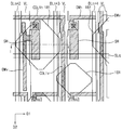
도 7은 본 발명의 일 실시예에 따른 표시 장치의 일 부분에서의 신호 배선들의 배열을 나타낸 평면도이다.
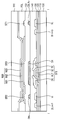
도 8는 도 7의 I-I'선을 따라 절단한 표시 장치의 단면도이다.
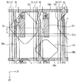
도 9은 도 7의 표시 장치의 다른 부분에서의 신호 배선들의 배열을 나타낸 평면도이다.
도 10는 도 9의 II-II'선을 따라 절단한 표시 장치의 단면도이다.
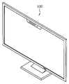
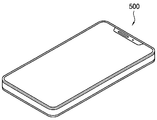
도 11은 본 발명의 실시예들에 따른 전자 기기를 나타내는 블록도이고, 도 12a는 도 11의 전자 기기가 텔레비전으로 구현된 일 예를 나타내는 도면이며, 도 12b는 도 11의 전자 기기가 스마트폰으로 구현된 일 예를 나타내는 도면이다.
120: 게이트 절연층 130: 층간 절연층
140: 제1 비아 절연층 150: 제2 비아 절연층
180: 발광 구조물 TFE: 박막 봉지층
TFT: 박막 트랜지스터 DLa, DLb: 데이터 라인
VL: 전원 배선 CDL: 우회 데이터 라인
DMh, DMv: 더미 패턴
Claims (20)
- 표시 영역 및 상기 표시 영역을 둘러싸는 비표시 영역인 주변 영역을 포함하는 베이스 기판;
상기 베이스 기판 상에 상기 표시 영역에 배치되고 상기 주변 영역까지 연장되는 복수의 데이터 라인들;
상기 베이스 기판 상에 상기 표시 영역 및 상기 주변 영역에 배치되고, 상기 데이터 라인들 중 적어도 하나와 전기적으로 연결되는 우회 데이터 라인; 및
상기 우회 데이터 라인과 이격되고 상기 우회 데이터 라인과 동일한 층에 배치되는 더미 패턴을 포함하는 표시 장치. - 제1 항에 있어서,
상기 더미 패턴에는 일정한 전압이 인가되는 것을 특징으로 하는 표시 장치. - 제2 항에 있어서,
상기 데이터 라인과 상기 우회 데이터 라인 사이에 배치되는 제1 비아 절연층;
상기 우회 데이터 라인 및 상기 더미 패턴이 배치된 상기 제1 비아 절연층 상에 배치되는 제2 비아 절연층;
상기 제2 비아 절연층 상에 배치되는 제1 전극;
상기 제1 전극 상에 배치되는 발광층; 및
상기 발광층 상에 배치되는 제2 전극을 더 포함하는 것을 특징으로 하는 표시 장치. - 제3 항에 있어서,
상기 베이스 기판과 상기 제1 비아 절연층 사이에 배치되고, 제1 전원 전압이 인가되는 제1 전원 배선을 더 포함하고,
상기 제1 전원 배선은 상기 우회 데이터 라인 또는 상기 더미 배선과 중첩하게 배치되는 것을 특징으로 하는 표시 장치. - 제3 항에 있어서,
상기 우회 데이터 라인과 상기 데이터 라인은 상기 주변 영역에서 상기 제1 비아 절연층을 통해 형성되는 컨택홀을 통해 서로 접하는 것을 특징으로 하는 표시 장치. - 제3 항에 있어서,
상기 제2 비아 절연층은 유기 절연 물질을 포함하는 것을 특징으로 하는 표시 장치. - 제6 항에 있어서,
상기 더미 패턴 및 상기 우회 데이터 라인 상의 상기 제2 비아 절연층의 상면에는 상기 더미 패턴 및 상기 우회 데이터 라인에 대응하는 단차가 형성되는 것을 특징으로 하는 표시 장치. - 제7 항에 있어서,
상기 제1 전극은 상기 더미 패턴 또는 상기 우회 데이터 라인과 적어도 일부가 중첩하도록 배치되어, 상기 제1 전극에도 상기 단차에 대응하는 단차가 형성되는 것을 특징으로 하는 표시 장치. - 제8 항에 있어서,
상기 제1 전극은 은(Ag)을 포함하는 것을 특징으로 하는 표시 장치. - 제1 항에 있어서,
상기 우회 데이터 라인은 수직부와 상기 수직부와 연결된 수평부를 포함하고,
상기 더미 패턴은 복수의 수직 더미부와 복수의 수평 더미부를 포함하고,
적어도 하나의 상기 수직 더미부는 상기 우회 데이터 라인의 상기 수직부와 일직선 상에 배치되고,
적어도 하나의 상기 수평 더미부는 상기 우회 데이터 라인의 상기 수평부와 일직선 상에 배치되는 것을 특징으로 하는 표시 장치. - 제1 항에 있어서,
상기 더미 패턴은 복수의 수직 더미부와 복수의 수평 더미부를 포함하고, 상기 수직 더미부와 상기 수평 더미부는 서로 연결되어 메쉬 구조를 이루는 것을 특징으로 하는 표시 장치. - 제1 항에 있어서,
상기 데이터 라인은 제n 데이터 라인과 제n+1 데이터 라인을 포함하고,
상기 우회 데이터 라인은 상기 제n 데이터 라인과 전기적으로 연결되는 제n 우회 데이터 라인 및 상기 제n+1 데이터 라인과 전기적으로 연결되는 제n+1 우회 데이터 라인을 포함하고,
상기 더미 패턴은 상기 제n 우회 데이터 라인과 상기 제n+1 우회 데이터 라인 사이에 배치되는 것을 특징으로 하는 표시 장치. - 제1 항에 있어서,
상기 표시 영역은 모서리가 둥근 사각형 형태이며,
상기 주변 영역은 패드부가 배치되기 위한 패드 영역을 포함하며,
상기 데이터 라인들은 상기 모서리에 인접하여 배치되는 제1 데이터 라인 및 상기 제1 데이터 라인과 이격되는 제2 데이터 라인을 포함하고,
상기 제1 데이터 라인은 상기 우회 데이터 라인을 통해 상기 패드부에 전기적으로 연결되고,
상기 제2 데이터 라인은 상기 우회 데이터 라인을 통하지 않고, 상기 패드부에 연결되는 것을 특징으로 하는 표시 장치. - 제1 항에 있어서,
상기 베이스 기판 상에 배치되는 박막 트랜지스터; 및
상기 더미 패턴과 물리적으로 연결되고, 상기 박막 트랜지스터와 중첩하게 배치되는 차폐 전극을 더 포함하는 것을 특징으로 하는 표시 장치. - 제1 항에 있어서,
상기 베이스 기판의 상기 주변 영역은 패드부가 배치되기 위한 패드 영역 및 상기 패드 영역을 상기 표시 장치의 후면에 배치시키기 위해 접히는 부분인 폴딩 영역을 더 포함하는 하는 것을 특징으로 하는 표시 장치. - 베이스 기판;
상기 베이스 기판 상에 배치되는 박막 트랜지스터;
상기 베이스 기판 상에 배치되는 층간 절연층;
상기 층간 절연층 상에 배치되는 제1 데이터 라인, 상기 제1 데이터 라인과 인접하는 제1 전원 배선, 제2 데이터 라인 및 상기 제2 데이터 라인과 인접하는 제2 전원 배선;
상기 제1 데이터 라인, 상기 제1 전원 배선, 상기 제2 데이터 라인 및 상기 제2 전원 배선 상에 배치되는 제1 비아 절연층;
상기 제1 비아 절연층 상에 배치되고, 상기 제1 데이터 라인과 전기적으로 연결되는 제1 우회 데이터 라인 및 더미 패턴; 및
상기 제1 우회 데이터 라인 및 상기 더미 패턴 상에 배치되고, 상기 제1 우회 데이터 라인 및 상기 더미 패턴의 프로파일을 따라 상면에 단차가 형성된 제2 비아 절연층을 포함하는 표시 장치. - 제16 항에 있어서,
상기 제2 비아 절연층 상에 배치되는 제1 전극;
상기 제1 전극 상에 배치되는 발광층; 및
상기 발광층 상에 배치되는 제2 전극을 포함하는 표시 장치. - 제17 항에 있어서,
상기 제1 전극은 상기 제1 우회 데이터 라인 또는 상기 더미 패턴과 중첩하는 것을 특징으로 하는 것을 특징으로 하는 표시 장치. - 제16 항에 있어서,
상기 더미 패턴에는 일정한 전압이 인가되는 것을 특징으로 하는 표시 장치. - 제16 항에 있어서,
상기 제2 비아 절연층은 유기 절연 물질을 포함하는 것을 특징으로 하는 표시 장치.
Priority Applications (7)
| Application Number | Priority Date | Filing Date | Title |
|---|---|---|---|
| KR1020180130766A KR102555841B1 (ko) | 2018-10-30 | 2018-10-30 | 표시 장치 |
| US17/290,732 US11957034B2 (en) | 2018-10-30 | 2019-09-24 | Display apparatus having an improved display quality and a reduced peripheral (non-display) region for use in electronic device having a bypass data line arranged in the display and peripheral regions |
| CN201980072456.XA CN113039648B (zh) | 2018-10-30 | 2019-09-24 | 显示装置 |
| PCT/KR2019/012423 WO2020091228A1 (ko) | 2018-10-30 | 2019-09-24 | 표시 장치 |
| EP19879989.2A EP3876282A4 (en) | 2018-10-30 | 2019-09-24 | INDICATOR |
| KR1020230089708A KR102804879B1 (ko) | 2018-10-30 | 2023-07-11 | 표시 장치 |
| US18/628,892 US12626642B2 (en) | 2018-10-30 | 2024-04-08 | Display apparatus having reduced non-display region |
Applications Claiming Priority (1)
| Application Number | Priority Date | Filing Date | Title |
|---|---|---|---|
| KR1020180130766A KR102555841B1 (ko) | 2018-10-30 | 2018-10-30 | 표시 장치 |
Related Child Applications (1)
| Application Number | Title | Priority Date | Filing Date |
|---|---|---|---|
| KR1020230089708A Division KR102804879B1 (ko) | 2018-10-30 | 2023-07-11 | 표시 장치 |
Publications (2)
| Publication Number | Publication Date |
|---|---|
| KR20200049979A true KR20200049979A (ko) | 2020-05-11 |
| KR102555841B1 KR102555841B1 (ko) | 2023-07-17 |
Family
ID=70462589
Family Applications (2)
| Application Number | Title | Priority Date | Filing Date |
|---|---|---|---|
| KR1020180130766A Active KR102555841B1 (ko) | 2018-10-30 | 2018-10-30 | 표시 장치 |
| KR1020230089708A Active KR102804879B1 (ko) | 2018-10-30 | 2023-07-11 | 표시 장치 |
Family Applications After (1)
| Application Number | Title | Priority Date | Filing Date |
|---|---|---|---|
| KR1020230089708A Active KR102804879B1 (ko) | 2018-10-30 | 2023-07-11 | 표시 장치 |
Country Status (5)
| Country | Link |
|---|---|
| US (2) | US11957034B2 (ko) |
| EP (1) | EP3876282A4 (ko) |
| KR (2) | KR102555841B1 (ko) |
| CN (1) | CN113039648B (ko) |
| WO (1) | WO2020091228A1 (ko) |
Cited By (2)
| Publication number | Priority date | Publication date | Assignee | Title |
|---|---|---|---|---|
| KR20230097420A (ko) * | 2021-12-24 | 2023-07-03 | 엘지디스플레이 주식회사 | 화소 구동 회로 및 발광 소자를 포함하는 디스플레이 장치 |
| US12462745B2 (en) | 2021-04-06 | 2025-11-04 | Samsung Display Co., Ltd. | Display apparatus |
Families Citing this family (15)
| Publication number | Priority date | Publication date | Assignee | Title |
|---|---|---|---|---|
| KR102555841B1 (ko) * | 2018-10-30 | 2023-07-17 | 삼성디스플레이 주식회사 | 표시 장치 |
| KR102800154B1 (ko) | 2019-03-29 | 2025-04-29 | 삼성디스플레이 주식회사 | 표시 장치 |
| KR102772543B1 (ko) * | 2019-06-13 | 2025-02-26 | 삼성디스플레이 주식회사 | 표시 장치 |
| KR102827182B1 (ko) * | 2020-05-29 | 2025-07-02 | 삼성디스플레이 주식회사 | 디스플레이 장치 |
| CN113903768B (zh) * | 2020-06-22 | 2025-01-10 | 上海和辉光电股份有限公司 | 阵列基板、柔性显示面板及显示装置 |
| EP4206810B1 (en) * | 2021-04-30 | 2026-04-08 | BOE Technology Group Co., Ltd. | Array substrate and display device |
| KR20230088529A (ko) * | 2021-12-10 | 2023-06-20 | 삼성디스플레이 주식회사 | 표시 장치 |
| CN114864640B (zh) * | 2022-04-20 | 2024-11-19 | 武汉华星光电半导体显示技术有限公司 | 一种显示面板及显示装置 |
| US20250143108A1 (en) * | 2022-05-20 | 2025-05-01 | Chengdu Boe Optoelectronics Technology Co., Ltd. | Display panel and display device |
| US20230397462A1 (en) * | 2022-06-03 | 2023-12-07 | Samsung Display Co., Ltd. | Display device |
| CN117751702B (zh) * | 2022-06-23 | 2026-03-31 | 北京小米移动软件有限公司 | 一种显示面板、显示屏及电子设备 |
| CN114974119B (zh) * | 2022-06-29 | 2024-06-14 | 上海天马微电子有限公司 | 显示面板及显示装置 |
| WO2024096474A1 (ko) | 2022-10-31 | 2024-05-10 | (주)유니테크쓰리디피 | 3d 프린팅 장치 |
| KR20240092973A (ko) * | 2022-12-15 | 2024-06-24 | 엘지디스플레이 주식회사 | 디스플레이 장치 및 디스플레이 패널 |
| KR20240174935A (ko) | 2023-06-09 | 2024-12-18 | 삼성디스플레이 주식회사 | 표시 장치 |
Citations (4)
| Publication number | Priority date | Publication date | Assignee | Title |
|---|---|---|---|---|
| KR20150025902A (ko) * | 2013-08-30 | 2015-03-11 | 엘지디스플레이 주식회사 | 유기발광 다이오드 디스플레이 장치 및 그 제조방법 |
| KR20170077780A (ko) * | 2015-12-28 | 2017-07-06 | 엘지디스플레이 주식회사 | 디스플레이 디바이스 |
| KR20170143066A (ko) * | 2016-06-17 | 2017-12-29 | 삼성디스플레이 주식회사 | 표시 패널, 및 이를 포함하는 전자 기기 |
| WO2018062023A1 (ja) * | 2016-09-27 | 2018-04-05 | シャープ株式会社 | 表示パネル |
Family Cites Families (20)
| Publication number | Priority date | Publication date | Assignee | Title |
|---|---|---|---|---|
| KR20050051504A (ko) | 2003-11-27 | 2005-06-01 | 삼성에스디아이 주식회사 | 유기전계발광표시장치의 전자파차폐구조 |
| KR101290078B1 (ko) | 2013-04-02 | 2013-07-26 | 주식회사 트레이스 | 베젤의 폭을 줄인 터치스크린 패널 및 그 제조방법 |
| JP6136578B2 (ja) | 2013-05-29 | 2017-05-31 | ソニー株式会社 | 表示装置および表示装置の製造方法ならびに電子機器 |
| KR102278601B1 (ko) * | 2014-03-07 | 2021-07-19 | 삼성디스플레이 주식회사 | 유기 발광 표시 장치 |
| KR102271114B1 (ko) * | 2014-03-28 | 2021-06-30 | 삼성디스플레이 주식회사 | 터치 감지 패널 |
| KR102463838B1 (ko) | 2015-08-24 | 2022-11-04 | 삼성디스플레이 주식회사 | 가요성 표시 장치와 이의 제조 방법 |
| KR102668839B1 (ko) | 2015-12-18 | 2024-05-22 | 엘지디스플레이 주식회사 | 디스플레이 디바이스 |
| US10067585B2 (en) | 2015-12-28 | 2018-09-04 | Lg Display Co., Ltd. | Display device with multilayered capacitor |
| KR102387791B1 (ko) * | 2015-12-31 | 2022-04-15 | 엘지디스플레이 주식회사 | 유기전계 발광표시장치 및 그 제조방법 |
| KR102137897B1 (ko) * | 2016-01-21 | 2020-08-13 | 애플 인크. | 유기 발광 다이오드 디스플레이들을 위한 전력 및 데이터 라우팅 구조들 |
| KR102600289B1 (ko) | 2016-09-21 | 2023-11-13 | 삼성디스플레이 주식회사 | 표시 장치 |
| KR102311316B1 (ko) | 2017-04-24 | 2021-10-13 | 삼성디스플레이 주식회사 | 표시장치 및 그 제조방법 |
| KR102460555B1 (ko) | 2018-01-03 | 2022-10-31 | 삼성디스플레이 주식회사 | 표시 장치 |
| CN108254984B (zh) * | 2018-01-31 | 2021-06-04 | 上海天马微电子有限公司 | 一种显示面板及显示装置 |
| KR102528500B1 (ko) * | 2018-07-19 | 2023-05-04 | 삼성디스플레이 주식회사 | 표시 장치 |
| KR102797644B1 (ko) * | 2018-08-07 | 2025-04-18 | 삼성디스플레이 주식회사 | 표시 장치 |
| KR102562837B1 (ko) | 2018-09-13 | 2023-08-03 | 삼성디스플레이 주식회사 | 유기 발광 표시 장치 |
| KR102555841B1 (ko) | 2018-10-30 | 2023-07-17 | 삼성디스플레이 주식회사 | 표시 장치 |
| KR102800154B1 (ko) | 2019-03-29 | 2025-04-29 | 삼성디스플레이 주식회사 | 표시 장치 |
| KR102772543B1 (ko) * | 2019-06-13 | 2025-02-26 | 삼성디스플레이 주식회사 | 표시 장치 |
-
2018
- 2018-10-30 KR KR1020180130766A patent/KR102555841B1/ko active Active
-
2019
- 2019-09-24 EP EP19879989.2A patent/EP3876282A4/en active Pending
- 2019-09-24 CN CN201980072456.XA patent/CN113039648B/zh active Active
- 2019-09-24 WO PCT/KR2019/012423 patent/WO2020091228A1/ko not_active Ceased
- 2019-09-24 US US17/290,732 patent/US11957034B2/en active Active
-
2023
- 2023-07-11 KR KR1020230089708A patent/KR102804879B1/ko active Active
-
2024
- 2024-04-08 US US18/628,892 patent/US12626642B2/en active Active
Patent Citations (4)
| Publication number | Priority date | Publication date | Assignee | Title |
|---|---|---|---|---|
| KR20150025902A (ko) * | 2013-08-30 | 2015-03-11 | 엘지디스플레이 주식회사 | 유기발광 다이오드 디스플레이 장치 및 그 제조방법 |
| KR20170077780A (ko) * | 2015-12-28 | 2017-07-06 | 엘지디스플레이 주식회사 | 디스플레이 디바이스 |
| KR20170143066A (ko) * | 2016-06-17 | 2017-12-29 | 삼성디스플레이 주식회사 | 표시 패널, 및 이를 포함하는 전자 기기 |
| WO2018062023A1 (ja) * | 2016-09-27 | 2018-04-05 | シャープ株式会社 | 表示パネル |
Cited By (2)
| Publication number | Priority date | Publication date | Assignee | Title |
|---|---|---|---|---|
| US12462745B2 (en) | 2021-04-06 | 2025-11-04 | Samsung Display Co., Ltd. | Display apparatus |
| KR20230097420A (ko) * | 2021-12-24 | 2023-07-03 | 엘지디스플레이 주식회사 | 화소 구동 회로 및 발광 소자를 포함하는 디스플레이 장치 |
Also Published As
| Publication number | Publication date |
|---|---|
| KR20230109127A (ko) | 2023-07-19 |
| EP3876282A4 (en) | 2022-08-17 |
| KR102804879B1 (ko) | 2025-05-12 |
| US20240260441A1 (en) | 2024-08-01 |
| CN113039648A (zh) | 2021-06-25 |
| KR102555841B1 (ko) | 2023-07-17 |
| US11957034B2 (en) | 2024-04-09 |
| CN113039648B (zh) | 2024-10-18 |
| EP3876282A1 (en) | 2021-09-08 |
| US12626642B2 (en) | 2026-05-12 |
| WO2020091228A1 (ko) | 2020-05-07 |
| US20220005886A1 (en) | 2022-01-06 |
Similar Documents
| Publication | Publication Date | Title |
|---|---|---|
| KR102804879B1 (ko) | 표시 장치 | |
| KR102632740B1 (ko) | 표시 장치 | |
| CN113130593B (zh) | 显示装置及制造显示装置的方法 | |
| CN110660812B (zh) | 显示装置 | |
| KR102800154B1 (ko) | 표시 장치 | |
| KR102773186B1 (ko) | 표시 장치 및 이의 제조 방법 | |
| KR102748388B1 (ko) | 표시 장치 및 이의 제조 방법 | |
| US12628505B2 (en) | Display apparatus | |
| KR102687808B1 (ko) | 표시 장치 | |
| KR102789415B1 (ko) | 표시 장치 및 이의 제조 방법 | |
| CN112838107A (zh) | 显示装置 | |
| KR20200084964A (ko) | 표시 장치 및 이의 제조 방법 | |
| KR20200047832A (ko) | 표시 장치 및 이의 제조 방법 | |
| KR102866567B1 (ko) | 표시 장치 | |
| KR102832109B1 (ko) | 표시 장치 | |
| KR102792806B1 (ko) | 표시 장치 | |
| CN111146253B (zh) | 显示装置 | |
| KR102606687B1 (ko) | 표시 장치 및 이의 제조 방법 |
Legal Events
| Date | Code | Title | Description |
|---|---|---|---|
| PA0109 | Patent application |
St.27 status event code: A-0-1-A10-A12-nap-PA0109 |
|
| R18-X000 | Changes to party contact information recorded |
St.27 status event code: A-3-3-R10-R18-oth-X000 |
|
| PG1501 | Laying open of application |
St.27 status event code: A-1-1-Q10-Q12-nap-PG1501 |
|
| A201 | Request for examination | ||
| PA0201 | Request for examination |
St.27 status event code: A-1-2-D10-D11-exm-PA0201 |
|
| E902 | Notification of reason for refusal | ||
| PE0902 | Notice of grounds for rejection |
St.27 status event code: A-1-2-D10-D21-exm-PE0902 |
|
| E13-X000 | Pre-grant limitation requested |
St.27 status event code: A-2-3-E10-E13-lim-X000 |
|
| P11-X000 | Amendment of application requested |
St.27 status event code: A-2-2-P10-P11-nap-X000 |
|
| P13-X000 | Application amended |
St.27 status event code: A-2-2-P10-P13-nap-X000 |
|
| P22-X000 | Classification modified |
St.27 status event code: A-2-2-P10-P22-nap-X000 |
|
| P22-X000 | Classification modified |
St.27 status event code: A-2-2-P10-P22-nap-X000 |
|
| E701 | Decision to grant or registration of patent right | ||
| PE0701 | Decision of registration |
St.27 status event code: A-1-2-D10-D22-exm-PE0701 |
|
| A107 | Divisional application of patent | ||
| GRNT | Written decision to grant | ||
| PA0107 | Divisional application |
St.27 status event code: A-0-1-A10-A18-div-PA0107 St.27 status event code: A-0-1-A10-A16-div-PA0107 |
|
| PR0701 | Registration of establishment |
St.27 status event code: A-2-4-F10-F11-exm-PR0701 |
|
| PR1002 | Payment of registration fee |
St.27 status event code: A-2-2-U10-U11-oth-PR1002 Fee payment year number: 1 |
|
| PG1601 | Publication of registration |
St.27 status event code: A-4-4-Q10-Q13-nap-PG1601 |
|
| P22-X000 | Classification modified |
St.27 status event code: A-4-4-P10-P22-nap-X000 |