KR20200051947A - 스퍼터링 장치 - Google Patents
스퍼터링 장치 Download PDFInfo
- Publication number
- KR20200051947A KR20200051947A KR1020180134899A KR20180134899A KR20200051947A KR 20200051947 A KR20200051947 A KR 20200051947A KR 1020180134899 A KR1020180134899 A KR 1020180134899A KR 20180134899 A KR20180134899 A KR 20180134899A KR 20200051947 A KR20200051947 A KR 20200051947A
- Authority
- KR
- South Korea
- Prior art keywords
- magnet
- cylindrical tube
- substrate
- pair
- substrate support
- Prior art date
- Legal status (The legal status is an assumption and is not a legal conclusion. Google has not performed a legal analysis and makes no representation as to the accuracy of the status listed.)
- Ceased
Links
- 238000004544 sputter deposition Methods 0.000 title claims abstract description 62
- 239000000758 substrate Substances 0.000 claims abstract description 85
- 230000001678 irradiating effect Effects 0.000 claims 1
- 230000002093 peripheral effect Effects 0.000 abstract description 2
- 239000010409 thin film Substances 0.000 description 16
- 238000000926 separation method Methods 0.000 description 10
- 239000011368 organic material Substances 0.000 description 9
- 230000008859 change Effects 0.000 description 7
- 238000000151 deposition Methods 0.000 description 6
- 239000007789 gas Substances 0.000 description 6
- 238000000034 method Methods 0.000 description 6
- 239000002245 particle Substances 0.000 description 5
- 238000012360 testing method Methods 0.000 description 5
- 230000008021 deposition Effects 0.000 description 4
- 238000010586 diagram Methods 0.000 description 3
- 238000001755 magnetron sputter deposition Methods 0.000 description 3
- 239000000463 material Substances 0.000 description 3
- 238000002294 plasma sputter deposition Methods 0.000 description 3
- 230000008569 process Effects 0.000 description 3
- 239000003507 refrigerant Substances 0.000 description 3
- 229910052710 silicon Inorganic materials 0.000 description 3
- 239000013077 target material Substances 0.000 description 3
- TVIVIEFSHFOWTE-UHFFFAOYSA-K tri(quinolin-8-yloxy)alumane Chemical compound [Al+3].C1=CN=C2C([O-])=CC=CC2=C1.C1=CN=C2C([O-])=CC=CC2=C1.C1=CN=C2C([O-])=CC=CC2=C1 TVIVIEFSHFOWTE-UHFFFAOYSA-K 0.000 description 3
- 235000012431 wafers Nutrition 0.000 description 3
- XKRFYHLGVUSROY-UHFFFAOYSA-N Argon Chemical compound [Ar] XKRFYHLGVUSROY-UHFFFAOYSA-N 0.000 description 2
- XUIMIQQOPSSXEZ-UHFFFAOYSA-N Silicon Chemical compound [Si] XUIMIQQOPSSXEZ-UHFFFAOYSA-N 0.000 description 2
- 229910052782 aluminium Inorganic materials 0.000 description 2
- 229910052802 copper Inorganic materials 0.000 description 2
- 239000010949 copper Substances 0.000 description 2
- 230000007423 decrease Effects 0.000 description 2
- 238000013461 design Methods 0.000 description 2
- 239000010408 film Substances 0.000 description 2
- 230000014509 gene expression Effects 0.000 description 2
- 239000011521 glass Substances 0.000 description 2
- 229910052737 gold Inorganic materials 0.000 description 2
- 239000010931 gold Substances 0.000 description 2
- 238000004519 manufacturing process Methods 0.000 description 2
- 239000007769 metal material Substances 0.000 description 2
- 238000012986 modification Methods 0.000 description 2
- 230000004048 modification Effects 0.000 description 2
- 238000005240 physical vapour deposition Methods 0.000 description 2
- 239000011241 protective layer Substances 0.000 description 2
- 239000004065 semiconductor Substances 0.000 description 2
- 239000010703 silicon Substances 0.000 description 2
- 239000000126 substance Substances 0.000 description 2
- 229910052715 tantalum Inorganic materials 0.000 description 2
- RYGMFSIKBFXOCR-UHFFFAOYSA-N Copper Chemical compound [Cu] RYGMFSIKBFXOCR-UHFFFAOYSA-N 0.000 description 1
- 239000000956 alloy Substances 0.000 description 1
- 229910045601 alloy Inorganic materials 0.000 description 1
- XAGFODPZIPBFFR-UHFFFAOYSA-N aluminium Chemical compound [Al] XAGFODPZIPBFFR-UHFFFAOYSA-N 0.000 description 1
- 229910052786 argon Inorganic materials 0.000 description 1
- 229910052799 carbon Inorganic materials 0.000 description 1
- 229910052804 chromium Inorganic materials 0.000 description 1
- 230000000052 comparative effect Effects 0.000 description 1
- 238000007599 discharging Methods 0.000 description 1
- 238000005516 engineering process Methods 0.000 description 1
- 230000008020 evaporation Effects 0.000 description 1
- 238000001704 evaporation Methods 0.000 description 1
- 238000002474 experimental method Methods 0.000 description 1
- 230000004907 flux Effects 0.000 description 1
- PCHJSUWPFVWCPO-UHFFFAOYSA-N gold Chemical compound [Au] PCHJSUWPFVWCPO-UHFFFAOYSA-N 0.000 description 1
- 229910052738 indium Inorganic materials 0.000 description 1
- 239000011261 inert gas Substances 0.000 description 1
- 238000002347 injection Methods 0.000 description 1
- 239000007924 injection Substances 0.000 description 1
- 150000002500 ions Chemical class 0.000 description 1
- 229910052749 magnesium Inorganic materials 0.000 description 1
- 230000008018 melting Effects 0.000 description 1
- 238000002844 melting Methods 0.000 description 1
- 229910052751 metal Inorganic materials 0.000 description 1
- 239000002184 metal Substances 0.000 description 1
- 229910044991 metal oxide Inorganic materials 0.000 description 1
- 150000004706 metal oxides Chemical class 0.000 description 1
- 229910052750 molybdenum Inorganic materials 0.000 description 1
- 229910052758 niobium Inorganic materials 0.000 description 1
- 150000004767 nitrides Chemical class 0.000 description 1
- 229910052763 palladium Inorganic materials 0.000 description 1
- 238000005424 photoluminescence Methods 0.000 description 1
- 229910052697 platinum Inorganic materials 0.000 description 1
- 239000002994 raw material Substances 0.000 description 1
- 229910052709 silver Inorganic materials 0.000 description 1
- GUVRBAGPIYLISA-UHFFFAOYSA-N tantalum atom Chemical compound [Ta] GUVRBAGPIYLISA-UHFFFAOYSA-N 0.000 description 1
- 229910052718 tin Inorganic materials 0.000 description 1
- 229910052719 titanium Inorganic materials 0.000 description 1
- 238000012546 transfer Methods 0.000 description 1
- 229910052721 tungsten Inorganic materials 0.000 description 1
- 229910052720 vanadium Inorganic materials 0.000 description 1
- 229910052725 zinc Inorganic materials 0.000 description 1
- 229910052726 zirconium Inorganic materials 0.000 description 1
Images

Classifications
-
- C—CHEMISTRY; METALLURGY
- C23—COATING METALLIC MATERIAL; COATING MATERIAL WITH METALLIC MATERIAL; CHEMICAL SURFACE TREATMENT; DIFFUSION TREATMENT OF METALLIC MATERIAL; COATING BY VACUUM EVAPORATION, BY SPUTTERING, BY ION IMPLANTATION OR BY CHEMICAL VAPOUR DEPOSITION, IN GENERAL; INHIBITING CORROSION OF METALLIC MATERIAL OR INCRUSTATION IN GENERAL
- C23C—COATING METALLIC MATERIAL; COATING MATERIAL WITH METALLIC MATERIAL; SURFACE TREATMENT OF METALLIC MATERIAL BY DIFFUSION INTO THE SURFACE, BY CHEMICAL CONVERSION OR SUBSTITUTION; COATING BY VACUUM EVAPORATION, BY SPUTTERING, BY ION IMPLANTATION OR BY CHEMICAL VAPOUR DEPOSITION, IN GENERAL
- C23C14/00—Coating by vacuum evaporation, by sputtering or by ion implantation of the coating forming material
- C23C14/22—Coating by vacuum evaporation, by sputtering or by ion implantation of the coating forming material characterised by the process of coating
- C23C14/34—Sputtering
- C23C14/35—Sputtering by application of a magnetic field, e.g. magnetron sputtering
- C23C14/354—Introduction of auxiliary energy into the plasma
- C23C14/357—Microwaves, e.g. electron cyclotron resonance enhanced sputtering
-
- C—CHEMISTRY; METALLURGY
- C23—COATING METALLIC MATERIAL; COATING MATERIAL WITH METALLIC MATERIAL; CHEMICAL SURFACE TREATMENT; DIFFUSION TREATMENT OF METALLIC MATERIAL; COATING BY VACUUM EVAPORATION, BY SPUTTERING, BY ION IMPLANTATION OR BY CHEMICAL VAPOUR DEPOSITION, IN GENERAL; INHIBITING CORROSION OF METALLIC MATERIAL OR INCRUSTATION IN GENERAL
- C23C—COATING METALLIC MATERIAL; COATING MATERIAL WITH METALLIC MATERIAL; SURFACE TREATMENT OF METALLIC MATERIAL BY DIFFUSION INTO THE SURFACE, BY CHEMICAL CONVERSION OR SUBSTITUTION; COATING BY VACUUM EVAPORATION, BY SPUTTERING, BY ION IMPLANTATION OR BY CHEMICAL VAPOUR DEPOSITION, IN GENERAL
- C23C14/00—Coating by vacuum evaporation, by sputtering or by ion implantation of the coating forming material
- C23C14/22—Coating by vacuum evaporation, by sputtering or by ion implantation of the coating forming material characterised by the process of coating
- C23C14/34—Sputtering
- C23C14/3407—Cathode assembly for sputtering apparatus, e.g. Target
-
- C—CHEMISTRY; METALLURGY
- C23—COATING METALLIC MATERIAL; COATING MATERIAL WITH METALLIC MATERIAL; CHEMICAL SURFACE TREATMENT; DIFFUSION TREATMENT OF METALLIC MATERIAL; COATING BY VACUUM EVAPORATION, BY SPUTTERING, BY ION IMPLANTATION OR BY CHEMICAL VAPOUR DEPOSITION, IN GENERAL; INHIBITING CORROSION OF METALLIC MATERIAL OR INCRUSTATION IN GENERAL
- C23C—COATING METALLIC MATERIAL; COATING MATERIAL WITH METALLIC MATERIAL; SURFACE TREATMENT OF METALLIC MATERIAL BY DIFFUSION INTO THE SURFACE, BY CHEMICAL CONVERSION OR SUBSTITUTION; COATING BY VACUUM EVAPORATION, BY SPUTTERING, BY ION IMPLANTATION OR BY CHEMICAL VAPOUR DEPOSITION, IN GENERAL
- C23C14/00—Coating by vacuum evaporation, by sputtering or by ion implantation of the coating forming material
- C23C14/22—Coating by vacuum evaporation, by sputtering or by ion implantation of the coating forming material characterised by the process of coating
- C23C14/50—Substrate holders
-
- H—ELECTRICITY
- H01—ELECTRIC ELEMENTS
- H01J—ELECTRIC DISCHARGE TUBES OR DISCHARGE LAMPS
- H01J37/00—Discharge tubes with provision for introducing objects or material to be exposed to the discharge, e.g. for the purpose of examination or processing thereof
- H01J37/32—Gas-filled discharge tubes
- H01J37/32431—Constructional details of the reactor
- H01J37/3266—Magnetic control means
- H01J37/32678—Electron cyclotron resonance
-
- H—ELECTRICITY
- H01—ELECTRIC ELEMENTS
- H01J—ELECTRIC DISCHARGE TUBES OR DISCHARGE LAMPS
- H01J37/00—Discharge tubes with provision for introducing objects or material to be exposed to the discharge, e.g. for the purpose of examination or processing thereof
- H01J37/32—Gas-filled discharge tubes
- H01J37/34—Gas-filled discharge tubes operating with cathodic sputtering
- H01J37/3411—Constructional aspects of the reactor
- H01J37/3414—Targets
- H01J37/342—Hollow targets
-
- H—ELECTRICITY
- H01—ELECTRIC ELEMENTS
- H01J—ELECTRIC DISCHARGE TUBES OR DISCHARGE LAMPS
- H01J37/00—Discharge tubes with provision for introducing objects or material to be exposed to the discharge, e.g. for the purpose of examination or processing thereof
- H01J37/32—Gas-filled discharge tubes
- H01J37/34—Gas-filled discharge tubes operating with cathodic sputtering
- H01J37/3411—Constructional aspects of the reactor
- H01J37/345—Magnet arrangements in particular for cathodic sputtering apparatus
- H01J37/3452—Magnet distribution
Landscapes
- Chemical & Material Sciences (AREA)
- Engineering & Computer Science (AREA)
- Physics & Mathematics (AREA)
- Plasma & Fusion (AREA)
- Analytical Chemistry (AREA)
- Chemical Kinetics & Catalysis (AREA)
- Materials Engineering (AREA)
- Mechanical Engineering (AREA)
- Metallurgy (AREA)
- Organic Chemistry (AREA)
- Physical Vapour Deposition (AREA)
Abstract
Description
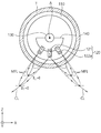
도 2는 도 1에서 도시된 본 스퍼터링 장치의 요부를 확대한 도면으로서, 연결선이 발산하는 모양을 도시한 개념도이다.
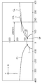
도 3은 도 2에서 도시된 연결선에 따른 플라즈마 발산각도를 설명하기 위한 개념도이다.
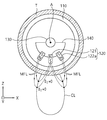
도 4는 도 2와 대비하여, 종래 스퍼터링 장치의 요부를 확대한 도면으로서, 연결선이 발산하지 않는 모양을 도시한 개념도이다.
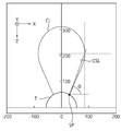
도 5는 도 4에서 도시된 연결선에 따른 플라즈마 발산각도를 설명하기 위한 개념도이다.
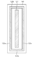
도 6은 1 또는 도 2에서 도시된 자석부의 저면도이다.
| T-S 이격거리(mm) | 방전 유무 | 기판 진입 전후의 전압변화량(△V) | 형성된 박막두께(Å) |
| 150 | X | - | - |
| 240 | O | 4 | 820 |
| 360 | O | 2 | 684 |
| Type | 플라즈마 발산각도 | T-S 이격거리(mm) | 기판 진입 전후의 전압변화량(△V) |
| 종래 스퍼터링장치 | 65° | 240 | 2 |
| 본 발명의 스퍼터링장치 | 26° | 150 | 10 |
| 26° | 90 | 40 |
| No. | H/W | PL(Photoluminescence Intensity) | Ratio(%) | 비고 | ||
| 자석세기(G) | 플라즈마 발산각도 |
T-S 이격거리(mm) | ||||
| 1 | - | 4669 | - | Alq3 Ref. | ||
| 2 | 600 | 70 | 1373 | 29.4 | Alq3+TCO | |
| 3 | 1800 | 10 | 150 | 방전X | - | |
| 3 | 1800 | 15 | 150 | 3085 | 66 | |
| 4 | 1800 | 26 | 150 | 3317 | 71 | |
| 5 | 1800 | 26 | 150 | 3255 | 69.7 | |
| 6 | 1800 | 45 | 150 | 3232 | 69.2 | |
| 7 | 1800 | 50 | 150 | 3309 | 70.9 | |
| 8 | 1800 | 55 | 150 | 2318 | 49.6 | |
110: 원통형의 튜브 120: 자석부
121: 제1 자석 122: 제2 자석
122a: 제2 자석 부분 122b: 연결 자석 부분
130: 요크 140: 고정 부재
150: 기판 지지부 160: 웨이브 가이드
170: 마이크로웨이브 조사부
A: 중심축 S: 기판
T: 타겟 MFL: 자기력선
CL: 연결선 SP: 시작점
Claims (6)
- 중심축이 Y축 방향으로 배치되고, 외주면에 타겟이 부착되는 원통형의 튜브;
상기 원통형의 튜브와 Z축 방향으로 이격되어 배치되며, XY 평면에 기판을 지지하는 기판 지지부;
상기 원통형의 튜브를 중심으로 서로 반대측에 대칭적으로 배치되는 한 쌍의 웨이브 가이드;
상기 한 쌍의 웨이브가이드를 통해서 전송되는 마이크로웨이브를 각각 상기 원통형의 튜브의 하측으로 조사하기 위한 한 쌍의 마이크로웨이브 조사부; 및
상기 원통형의 튜브 내측에 배치되어, 상기 원통형의 튜브와 상기 기판 지지부 사이의 공간에 자기장을 형성하기 위한 자석부;
를 포함하고,
상기 자석부는,
Y축을 따라 연장되며, 제1 극이 상기 기판 지지부를 향하며, 상기 제1 극과 반대 극성의 제2 극이 상기 원통형의 튜브의 중심을 향하도록 배치된 제1 자석; 및
상기 제1 자석을 가운데 두고, 상기 제2 극이 상기 기판 지지부를 향하여 각도가 벌어지도록 배치된 한 쌍의 제2 자석 부분을 포함하며,
상기 제1 자석과 제2 자석 부분 사이에 형성되는 자기력선들의 수직성분이 존재하지 않는(Bz=0) 지점들을 연결하여 형성되는 연결선이 발산하는 것을 특징으로 하는 스퍼터링 장치.
- 제1 항에 있어서,
상기 연결선이 상기 타겟 표면으로부터 시작하는 시작점과 X축 방향으로 200mm 연결한 지점을 연결한 연결직선과, 상기 시작점으로부터 X축 방향으로 연장되는 선분과의 각도로 정의되는 플라즈마 발산각도는 15°내지 50°의 범위 내에 있는 것을 특징으로 하는 스퍼터링 장치.
- 제1 항에 있어서,
상기 연결선이 타겟 표면에서 시작되는 부분에서의 자기장의 세기는 1700G 내지 1900G 범위인 것을 특징으로 하는 스퍼터링 장치.
- 제1 항에 있어서,
상기 제1 자석의 세기는, 상기 제1 자석과 최근접의 타겟 표면 에서 1600G 내지 2200G의 범위이고,
상기 제2 자석의 세기는, 상기 제2 자석과 최근접의 타겟 표면에서 1000G 내지 1400G의 범위이며,
상기 연결선이 타겟 표면에서 시작되는 부분에서의 자기장의 세기는 1700G 내지 1900G 범위를 갖도록 상기 제1 자석과 상기 제2 자석 부분의 세기가 결정되는 것을 특징으로 하는 스퍼터링 장치.
- 제1 항에 있어서,
상기 원통형의 튜브는 상기 중심축을 중심으로 회전할 수 있도록 형성된 것을 특징으로 하는 스퍼터링 장치.
- 제1 항에 있어서,
마이크로웨이브의 조사각도를 조절할 수 있도록, 상기 마이크로웨이브 조사부는 회전가능하도록 장착된 것을 특징으로 하는 스퍼터링 장치.
Priority Applications (1)
| Application Number | Priority Date | Filing Date | Title |
|---|---|---|---|
| KR1020180134899A KR20200051947A (ko) | 2018-11-06 | 2018-11-06 | 스퍼터링 장치 |
Applications Claiming Priority (1)
| Application Number | Priority Date | Filing Date | Title |
|---|---|---|---|
| KR1020180134899A KR20200051947A (ko) | 2018-11-06 | 2018-11-06 | 스퍼터링 장치 |
Publications (1)
| Publication Number | Publication Date |
|---|---|
| KR20200051947A true KR20200051947A (ko) | 2020-05-14 |
Family
ID=70737080
Family Applications (1)
| Application Number | Title | Priority Date | Filing Date |
|---|---|---|---|
| KR1020180134899A Ceased KR20200051947A (ko) | 2018-11-06 | 2018-11-06 | 스퍼터링 장치 |
Country Status (1)
| Country | Link |
|---|---|
| KR (1) | KR20200051947A (ko) |
Cited By (2)
| Publication number | Priority date | Publication date | Assignee | Title |
|---|---|---|---|---|
| KR20230073099A (ko) * | 2021-11-18 | 2023-05-25 | 한국핵융합에너지연구원 | 플라즈마 스퍼터링 장치 |
| WO2023090835A1 (ko) * | 2021-11-18 | 2023-05-25 | 한국핵융합에너지연구원 | 플라즈마 스퍼터링 장치 |
Citations (1)
| Publication number | Priority date | Publication date | Assignee | Title |
|---|---|---|---|---|
| KR20150069073A (ko) | 2013-12-12 | 2015-06-23 | 한국기초과학지원연구원 | Ecr 플라즈마 스퍼터링 장치 |
-
2018
- 2018-11-06 KR KR1020180134899A patent/KR20200051947A/ko not_active Ceased
Patent Citations (1)
| Publication number | Priority date | Publication date | Assignee | Title |
|---|---|---|---|---|
| KR20150069073A (ko) | 2013-12-12 | 2015-06-23 | 한국기초과학지원연구원 | Ecr 플라즈마 스퍼터링 장치 |
Cited By (2)
| Publication number | Priority date | Publication date | Assignee | Title |
|---|---|---|---|---|
| KR20230073099A (ko) * | 2021-11-18 | 2023-05-25 | 한국핵융합에너지연구원 | 플라즈마 스퍼터링 장치 |
| WO2023090835A1 (ko) * | 2021-11-18 | 2023-05-25 | 한국핵융합에너지연구원 | 플라즈마 스퍼터링 장치 |
Similar Documents
| Publication | Publication Date | Title |
|---|---|---|
| EP2257964B1 (en) | Reactive sputtering with hipims | |
| US8110086B2 (en) | Method of manufacturing a process chamber component having yttrium-aluminum coating | |
| JP3737363B2 (ja) | 不均一性補償を伴う表面の物理的気相処理 | |
| US20070012558A1 (en) | Magnetron sputtering system for large-area substrates | |
| US12249537B2 (en) | Substrate flipping in vacuum for dual sided PVD sputtering | |
| KR20130035924A (ko) | 마그네트론 스퍼터 장치 및 방법 | |
| US11948784B2 (en) | Tilted PVD source with rotating pedestal | |
| US6200433B1 (en) | IMP technology with heavy gas sputtering | |
| US11688591B2 (en) | Physical vapor deposition apparatus and method thereof | |
| WO2018040408A1 (zh) | 一种磁控元件和磁控溅射装置 | |
| KR20200051947A (ko) | 스퍼터링 장치 | |
| CN120265823A (zh) | 用于在基板上沉积材料的系统与方法 | |
| US20240167147A1 (en) | Apparatus and methods for depositing material within a through via | |
| US6620298B1 (en) | Magnetron sputtering method and apparatus | |
| JP2001140066A (ja) | 薄膜形成方法及び形成装置 | |
| US12325909B2 (en) | EM source for enhanced plasma control | |
| US20060081466A1 (en) | High uniformity 1-D multiple magnet magnetron source | |
| US6244210B1 (en) | Strength coil for ionized copper plasma deposition | |
| US20240105425A1 (en) | Substrate processing apparatus and method of processing substrate by using the same | |
| US12195843B2 (en) | Multicathode PVD system for high aspect ratio barrier seed deposition | |
| US20240263299A1 (en) | Module for flipping substrates in vacuum | |
| TW202603196A (zh) | 改善階梯覆蓋及損傷控制之脈衝電壓波形遞送 | |
| JPH02148722A (ja) | 半導体集積回路装置の製造方法 | |
| JP2013001965A (ja) | スパッタリング方法 |
Legal Events
| Date | Code | Title | Description |
|---|---|---|---|
| PA0109 | Patent application |
Patent event code: PA01091R01D Comment text: Patent Application Patent event date: 20181106 |
|
| PA0201 | Request for examination | ||
| E902 | Notification of reason for refusal | ||
| PE0902 | Notice of grounds for rejection |
Comment text: Notification of reason for refusal Patent event date: 20200506 Patent event code: PE09021S01D |
|
| PG1501 | Laying open of application | ||
| E902 | Notification of reason for refusal | ||
| PE0902 | Notice of grounds for rejection |
Comment text: Notification of reason for refusal Patent event date: 20200804 Patent event code: PE09021S01D |
|
| E601 | Decision to refuse application | ||
| PE0601 | Decision on rejection of patent |
Patent event date: 20201021 Comment text: Decision to Refuse Application Patent event code: PE06012S01D Patent event date: 20200804 Comment text: Notification of reason for refusal Patent event code: PE06011S01I Patent event date: 20200506 Comment text: Notification of reason for refusal Patent event code: PE06011S01I |