KR20200052973A - 정전 척 어셈블리, 정전 척 및 포커스 링 - Google Patents
정전 척 어셈블리, 정전 척 및 포커스 링 Download PDFInfo
- Publication number
- KR20200052973A KR20200052973A KR1020207012239A KR20207012239A KR20200052973A KR 20200052973 A KR20200052973 A KR 20200052973A KR 1020207012239 A KR1020207012239 A KR 1020207012239A KR 20207012239 A KR20207012239 A KR 20207012239A KR 20200052973 A KR20200052973 A KR 20200052973A
- Authority
- KR
- South Korea
- Prior art keywords
- focus ring
- arrangement surface
- wafer
- electrostatic chuck
- electrode
- Prior art date
- Legal status (The legal status is an assumption and is not a legal conclusion. Google has not performed a legal analysis and makes no representation as to the accuracy of the status listed.)
- Granted
Links
Images

Classifications
-
- H01L21/6833—
-
- H—ELECTRICITY
- H10—SEMICONDUCTOR DEVICES; ELECTRIC SOLID-STATE DEVICES NOT OTHERWISE PROVIDED FOR
- H10P—GENERIC PROCESSES OR APPARATUS FOR THE MANUFACTURE OR TREATMENT OF DEVICES COVERED BY CLASS H10
- H10P72/00—Handling or holding of wafers, substrates or devices during manufacture or treatment thereof
- H10P72/70—Handling or holding of wafers, substrates or devices during manufacture or treatment thereof for supporting or gripping
- H10P72/72—Handling or holding of wafers, substrates or devices during manufacture or treatment thereof for supporting or gripping using electrostatic chucks
- H10P72/722—Details of electrostatic chucks
-
- B—PERFORMING OPERATIONS; TRANSPORTING
- B23—MACHINE TOOLS; METAL-WORKING NOT OTHERWISE PROVIDED FOR
- B23Q—DETAILS, COMPONENTS, OR ACCESSORIES FOR MACHINE TOOLS, e.g. ARRANGEMENTS FOR COPYING OR CONTROLLING; MACHINE TOOLS IN GENERAL CHARACTERISED BY THE CONSTRUCTION OF PARTICULAR DETAILS OR COMPONENTS; COMBINATIONS OR ASSOCIATIONS OF METAL-WORKING MACHINES, NOT DIRECTED TO A PARTICULAR RESULT
- B23Q3/00—Devices holding, supporting, or positioning work or tools, of a kind normally removable from the machine
- B23Q3/15—Devices for holding work using magnetic or electric force acting directly on the work
-
- H—ELECTRICITY
- H01—ELECTRIC ELEMENTS
- H01J—ELECTRIC DISCHARGE TUBES OR DISCHARGE LAMPS
- H01J37/00—Discharge tubes with provision for introducing objects or material to be exposed to the discharge, e.g. for the purpose of examination or processing thereof
- H01J37/32—Gas-filled discharge tubes
- H01J37/32431—Constructional details of the reactor
- H01J37/32623—Mechanical discharge control means
- H01J37/32642—Focus rings
-
- H—ELECTRICITY
- H01—ELECTRIC ELEMENTS
- H01J—ELECTRIC DISCHARGE TUBES OR DISCHARGE LAMPS
- H01J37/00—Discharge tubes with provision for introducing objects or material to be exposed to the discharge, e.g. for the purpose of examination or processing thereof
- H01J37/32—Gas-filled discharge tubes
- H01J37/32431—Constructional details of the reactor
- H01J37/32715—Workpiece holder
- H01J37/32724—Temperature
-
- H01L21/68735—
-
- H01L21/68785—
-
- H—ELECTRICITY
- H02—GENERATION; CONVERSION OR DISTRIBUTION OF ELECTRIC POWER
- H02N—ELECTRIC MACHINES NOT OTHERWISE PROVIDED FOR
- H02N13/00—Clutches or holding devices using electrostatic attraction, e.g. using Johnson-Rahbek effect
-
- H—ELECTRICITY
- H10—SEMICONDUCTOR DEVICES; ELECTRIC SOLID-STATE DEVICES NOT OTHERWISE PROVIDED FOR
- H10P—GENERIC PROCESSES OR APPARATUS FOR THE MANUFACTURE OR TREATMENT OF DEVICES COVERED BY CLASS H10
- H10P72/00—Handling or holding of wafers, substrates or devices during manufacture or treatment thereof
- H10P72/04—Apparatus for manufacture or treatment
- H10P72/0431—Apparatus for thermal treatment
- H10P72/0432—Apparatus for thermal treatment mainly by conduction
-
- H—ELECTRICITY
- H10—SEMICONDUCTOR DEVICES; ELECTRIC SOLID-STATE DEVICES NOT OTHERWISE PROVIDED FOR
- H10P—GENERIC PROCESSES OR APPARATUS FOR THE MANUFACTURE OR TREATMENT OF DEVICES COVERED BY CLASS H10
- H10P72/00—Handling or holding of wafers, substrates or devices during manufacture or treatment thereof
- H10P72/04—Apparatus for manufacture or treatment
- H10P72/0431—Apparatus for thermal treatment
- H10P72/0434—Apparatus for thermal treatment mainly by convection
-
- H—ELECTRICITY
- H10—SEMICONDUCTOR DEVICES; ELECTRIC SOLID-STATE DEVICES NOT OTHERWISE PROVIDED FOR
- H10P—GENERIC PROCESSES OR APPARATUS FOR THE MANUFACTURE OR TREATMENT OF DEVICES COVERED BY CLASS H10
- H10P72/00—Handling or holding of wafers, substrates or devices during manufacture or treatment thereof
- H10P72/04—Apparatus for manufacture or treatment
- H10P72/0441—Apparatus for sealing, encapsulating, glassing, decapsulating or the like
-
- H—ELECTRICITY
- H10—SEMICONDUCTOR DEVICES; ELECTRIC SOLID-STATE DEVICES NOT OTHERWISE PROVIDED FOR
- H10P—GENERIC PROCESSES OR APPARATUS FOR THE MANUFACTURE OR TREATMENT OF DEVICES COVERED BY CLASS H10
- H10P72/00—Handling or holding of wafers, substrates or devices during manufacture or treatment thereof
- H10P72/70—Handling or holding of wafers, substrates or devices during manufacture or treatment thereof for supporting or gripping
- H10P72/72—Handling or holding of wafers, substrates or devices during manufacture or treatment thereof for supporting or gripping using electrostatic chucks
-
- H—ELECTRICITY
- H10—SEMICONDUCTOR DEVICES; ELECTRIC SOLID-STATE DEVICES NOT OTHERWISE PROVIDED FOR
- H10P—GENERIC PROCESSES OR APPARATUS FOR THE MANUFACTURE OR TREATMENT OF DEVICES COVERED BY CLASS H10
- H10P72/00—Handling or holding of wafers, substrates or devices during manufacture or treatment thereof
- H10P72/70—Handling or holding of wafers, substrates or devices during manufacture or treatment thereof for supporting or gripping
- H10P72/76—Handling or holding of wafers, substrates or devices during manufacture or treatment thereof for supporting or gripping using mechanical means, e.g. clamps or pinches
- H10P72/7604—Handling or holding of wafers, substrates or devices during manufacture or treatment thereof for supporting or gripping using mechanical means, e.g. clamps or pinches the wafers being placed on a susceptor, stage or support
- H10P72/7611—Handling or holding of wafers, substrates or devices during manufacture or treatment thereof for supporting or gripping using mechanical means, e.g. clamps or pinches the wafers being placed on a susceptor, stage or support characterised by edge profile or support profile
-
- H—ELECTRICITY
- H10—SEMICONDUCTOR DEVICES; ELECTRIC SOLID-STATE DEVICES NOT OTHERWISE PROVIDED FOR
- H10P—GENERIC PROCESSES OR APPARATUS FOR THE MANUFACTURE OR TREATMENT OF DEVICES COVERED BY CLASS H10
- H10P72/00—Handling or holding of wafers, substrates or devices during manufacture or treatment thereof
- H10P72/70—Handling or holding of wafers, substrates or devices during manufacture or treatment thereof for supporting or gripping
- H10P72/76—Handling or holding of wafers, substrates or devices during manufacture or treatment thereof for supporting or gripping using mechanical means, e.g. clamps or pinches
- H10P72/7604—Handling or holding of wafers, substrates or devices during manufacture or treatment thereof for supporting or gripping using mechanical means, e.g. clamps or pinches the wafers being placed on a susceptor, stage or support
- H10P72/7614—Handling or holding of wafers, substrates or devices during manufacture or treatment thereof for supporting or gripping using mechanical means, e.g. clamps or pinches the wafers being placed on a susceptor, stage or support characterised by a plurality of individual support members, e.g. support posts or protrusions
-
- H—ELECTRICITY
- H10—SEMICONDUCTOR DEVICES; ELECTRIC SOLID-STATE DEVICES NOT OTHERWISE PROVIDED FOR
- H10P—GENERIC PROCESSES OR APPARATUS FOR THE MANUFACTURE OR TREATMENT OF DEVICES COVERED BY CLASS H10
- H10P72/00—Handling or holding of wafers, substrates or devices during manufacture or treatment thereof
- H10P72/70—Handling or holding of wafers, substrates or devices during manufacture or treatment thereof for supporting or gripping
- H10P72/76—Handling or holding of wafers, substrates or devices during manufacture or treatment thereof for supporting or gripping using mechanical means, e.g. clamps or pinches
- H10P72/7604—Handling or holding of wafers, substrates or devices during manufacture or treatment thereof for supporting or gripping using mechanical means, e.g. clamps or pinches the wafers being placed on a susceptor, stage or support
- H10P72/7616—Handling or holding of wafers, substrates or devices during manufacture or treatment thereof for supporting or gripping using mechanical means, e.g. clamps or pinches the wafers being placed on a susceptor, stage or support characterised by a coating, a hardness or a material
-
- H—ELECTRICITY
- H10—SEMICONDUCTOR DEVICES; ELECTRIC SOLID-STATE DEVICES NOT OTHERWISE PROVIDED FOR
- H10P—GENERIC PROCESSES OR APPARATUS FOR THE MANUFACTURE OR TREATMENT OF DEVICES COVERED BY CLASS H10
- H10P72/00—Handling or holding of wafers, substrates or devices during manufacture or treatment thereof
- H10P72/70—Handling or holding of wafers, substrates or devices during manufacture or treatment thereof for supporting or gripping
- H10P72/76—Handling or holding of wafers, substrates or devices during manufacture or treatment thereof for supporting or gripping using mechanical means, e.g. clamps or pinches
- H10P72/7604—Handling or holding of wafers, substrates or devices during manufacture or treatment thereof for supporting or gripping using mechanical means, e.g. clamps or pinches the wafers being placed on a susceptor, stage or support
- H10P72/7624—Handling or holding of wafers, substrates or devices during manufacture or treatment thereof for supporting or gripping using mechanical means, e.g. clamps or pinches the wafers being placed on a susceptor, stage or support characterised by the mechanical construction of the susceptor, stage or support
-
- H—ELECTRICITY
- H01—ELECTRIC ELEMENTS
- H01J—ELECTRIC DISCHARGE TUBES OR DISCHARGE LAMPS
- H01J2237/00—Discharge tubes exposing object to beam, e.g. for analysis treatment, etching, imaging
- H01J2237/002—Cooling arrangements
Landscapes
- Engineering & Computer Science (AREA)
- Physics & Mathematics (AREA)
- Plasma & Fusion (AREA)
- Chemical & Material Sciences (AREA)
- Analytical Chemistry (AREA)
- Mechanical Engineering (AREA)
- Container, Conveyance, Adherence, Positioning, Of Wafer (AREA)
- Drying Of Semiconductors (AREA)
Abstract
Description
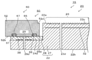
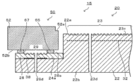
도 2는 도 1의 정전 척 어셈블리(15)의 부분 확대도이다.
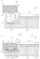
도 3은 정전 척 어셈블리(15)의 조립 순서를 도시한 설명도이다.
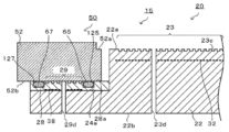
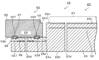
도 4는 정전 척 어셈블리(15)의 다른 예의 부분 확대도이다.
도 5는 정전 척 어셈블리(15)의 다른 예의 부분 확대도이다.
도 6은 정전 척 어셈블리(15)의 다른 예의 부분 확대도이다.
도 7은 정전 척 어셈블리(15)의 다른 예의 부분 확대도이다.
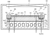
20: 정전 척 22: 세라믹체
22a: 웨이퍼 배치면 22b: 이면
23: 요철 영역 23c: 오목부
23d: 가스 공급로 24a: 환형 단차면
27: 제1 세라믹 부재 28: 제2 세라믹 부재
28a: 포커스 링 배치면 29: 요철 영역
29c: 오목부 29d: 가스 공급로
32: 웨이퍼 흡착용 전극 38: 포커스 링 흡착용 전극
50: 포커스 링 52: 링 본체
52a: 환형 단차면 52b: 이면
54: 대향 영역 55, 355: 내주홈
57, 357: 외주홈 60: O링
65: 소직경 O링 67: 대직경 O링
70: 냉각판 72: 냉매 통로
75: 본딩 시트 80: 챔버
90: 샤워 헤드 125, 325: 내주홈
127, 327: 외주홈 227, 255: 절결홈
W: 웨이퍼
Claims (4)
- 원형 표면인 웨이퍼 배치면과 비교하여 저위(低位)의 포커스 링 배치면을 상기 웨이퍼 배치면의 외주부에 갖는 세라믹체와,
상기 세라믹체의 내부 중 상기 웨이퍼 배치면에 대향하는 위치에 매설된 제1 전극과,
상기 세라믹체의 내부 중 상기 포커스 링 배치면에 대향하는 위치에 매설된 제2 전극과,
상기 포커스 링 배치면의 표면에 형성된 가스 저장용의 요철 영역과,
상기 포커스 링 배치면에 배치된 포커스 링과,
상기 포커스 링 배치면과 상기 포커스 링 사이이며 상기 요철 영역을 둘러싸도록 상기 포커스 링 배치면의 내주측 및 외주측에 배치된 한 쌍의 탄성 환형 시일재
를 구비한 정전 척 어셈블리. - 제1항에 있어서, 상기 탄성 환형 시일재는, 상기 포커스 링 배치면 및 상기 포커스 링 중 적어도 한쪽에 형성된 환형 홈에 끼워 넣어져 있는 것인 정전 척 어셈블리.
- 원형 표면인 웨이퍼 배치면과 비교하여 저위의 포커스 링 배치면을 상기 웨이퍼 배치면의 외주부에 갖는 세라믹체와,
상기 세라믹체의 내부 중 상기 웨이퍼 배치면에 대향하는 위치에 매설된 제1 전극과,
상기 세라믹체의 내부 중 상기 포커스 링 배치면에 대향하는 위치에 매설된 제2 전극과,
상기 포커스 링 배치면의 표면에 형성된 가스 저장용의 요철 영역과,
상기 포커스 링 배치면의 표면 중 상기 요철 영역을 둘러싸도록 내주측 및 외주측에 형성된 한 쌍의 환형 홈
을 구비한 정전 척. - 정전 척의 포커스 링 배치면에 배치되는 포커스 링으로서,
상기 포커스 링 중 상기 정전 척에 배치되는 측의 면의 내주측 및 외주측에 형성된 한 쌍의 환형 홈
을 구비하고,
상기 한 쌍의 환형 홈은, 상기 포커스 링 배치면에 형성된 가스 저장용의 요철 영역의 내주측과 외주측을 둘러싸는 것이 가능한 위치에 형성되어 있는 것인 포커스 링.
Applications Claiming Priority (3)
| Application Number | Priority Date | Filing Date | Title |
|---|---|---|---|
| US201762581900P | 2017-11-06 | 2017-11-06 | |
| US62/581,900 | 2017-11-06 | ||
| PCT/JP2018/040590 WO2019088204A1 (ja) | 2017-11-06 | 2018-10-31 | 静電チャックアセンブリ、静電チャック及びフォーカスリング |
Publications (2)
| Publication Number | Publication Date |
|---|---|
| KR20200052973A true KR20200052973A (ko) | 2020-05-15 |
| KR102387008B1 KR102387008B1 (ko) | 2022-04-18 |
Family
ID=66333588
Family Applications (1)
| Application Number | Title | Priority Date | Filing Date |
|---|---|---|---|
| KR1020207012239A Active KR102387008B1 (ko) | 2017-11-06 | 2018-10-31 | 정전 척 어셈블리, 정전 척 및 포커스 링 |
Country Status (6)
| Country | Link |
|---|---|
| US (1) | US11610798B2 (ko) |
| JP (1) | JP6894000B2 (ko) |
| KR (1) | KR102387008B1 (ko) |
| CN (1) | CN111226309B (ko) |
| TW (1) | TWI761621B (ko) |
| WO (1) | WO2019088204A1 (ko) |
Cited By (4)
| Publication number | Priority date | Publication date | Assignee | Title |
|---|---|---|---|---|
| KR20230026252A (ko) * | 2021-08-17 | 2023-02-24 | 엔지케이 인슐레이터 엘티디 | 웨이퍼 배치대 |
| KR20230141443A (ko) * | 2022-03-31 | 2023-10-10 | 엔지케이 인슐레이터 엘티디 | 웨이퍼 배치대 |
| KR20240174523A (ko) * | 2023-06-07 | 2024-12-17 | 엔지케이 인슐레이터 엘티디 | 웨이퍼 적재대 |
| US12548741B2 (en) | 2022-07-21 | 2026-02-10 | Solmics Co., Ltd. | Focus ring and plasma etching device including same |
Families Citing this family (57)
| Publication number | Priority date | Publication date | Assignee | Title |
|---|---|---|---|---|
| US10510575B2 (en) | 2017-09-20 | 2019-12-17 | Applied Materials, Inc. | Substrate support with multiple embedded electrodes |
| US10555412B2 (en) | 2018-05-10 | 2020-02-04 | Applied Materials, Inc. | Method of controlling ion energy distribution using a pulse generator with a current-return output stage |
| JP7204350B2 (ja) * | 2018-06-12 | 2023-01-16 | 東京エレクトロン株式会社 | 載置台、基板処理装置及びエッジリング |
| JP7228989B2 (ja) * | 2018-11-05 | 2023-02-27 | 東京エレクトロン株式会社 | 載置台、エッジリングの位置決め方法及び基板処理装置 |
| US11476145B2 (en) | 2018-11-20 | 2022-10-18 | Applied Materials, Inc. | Automatic ESC bias compensation when using pulsed DC bias |
| KR20250100790A (ko) | 2019-01-22 | 2025-07-03 | 어플라이드 머티어리얼스, 인코포레이티드 | 펄스 전압 파형을 제어하기 위한 피드백 루프 |
| US11508554B2 (en) | 2019-01-24 | 2022-11-22 | Applied Materials, Inc. | High voltage filter assembly |
| KR102277809B1 (ko) * | 2019-07-15 | 2021-07-14 | 세메스 주식회사 | 기판 지지 유닛 및 이를 구비하는 기판 처리 시스템 |
| JP7394556B2 (ja) * | 2019-08-09 | 2023-12-08 | 東京エレクトロン株式会社 | 載置台及び基板処理装置 |
| TWI748607B (zh) * | 2019-09-06 | 2021-12-01 | 日商Toto股份有限公司 | 靜電吸盤 |
| KR102697630B1 (ko) * | 2019-10-15 | 2024-08-23 | 삼성전자주식회사 | 식각 장치 |
| CN110634727B (zh) * | 2019-11-18 | 2020-02-21 | 中微半导体设备(上海)股份有限公司 | 一种等离子体处理装置及其调节方法 |
| JP7390880B2 (ja) | 2019-12-05 | 2023-12-04 | 東京エレクトロン株式会社 | エッジリング及び基板処理装置 |
| JP7308767B2 (ja) * | 2020-01-08 | 2023-07-14 | 東京エレクトロン株式会社 | 載置台およびプラズマ処理装置 |
| US11551916B2 (en) * | 2020-03-20 | 2023-01-10 | Applied Materials, Inc. | Sheath and temperature control of a process kit in a substrate processing chamber |
| JP7450427B2 (ja) | 2020-03-25 | 2024-03-15 | 東京エレクトロン株式会社 | 基板支持器及びプラズマ処理装置 |
| KR102902338B1 (ko) * | 2020-04-02 | 2025-12-18 | 램 리써치 코포레이션 | 통합된 시일들 (seals) 을 갖는 냉각된 에지 링 |
| US12597589B2 (en) * | 2020-06-29 | 2026-04-07 | Sumitomo Osaka Cement Co., Ltd. | Electrostatic chuck |
| US11848176B2 (en) | 2020-07-31 | 2023-12-19 | Applied Materials, Inc. | Plasma processing using pulsed-voltage and radio-frequency power |
| CN114188205B (zh) * | 2020-09-14 | 2024-12-10 | 中微半导体设备(上海)股份有限公司 | 一种静电装置、其所在的基片处理系统及其置换清洁方法 |
| KR102899162B1 (ko) * | 2020-09-14 | 2025-12-10 | 에이에스엠 아이피 홀딩 비.브이. | 플라즈마 장치용 서셉터 어셈블리 |
| CN112397366B (zh) * | 2020-11-05 | 2023-07-14 | 北京北方华创微电子装备有限公司 | 一种承载装置及半导体反应腔室 |
| JP6842225B1 (ja) * | 2020-11-12 | 2021-03-17 | ハイソル株式会社 | チャックユニット及びチャックユニットの温度制御方法 |
| US11798790B2 (en) | 2020-11-16 | 2023-10-24 | Applied Materials, Inc. | Apparatus and methods for controlling ion energy distribution |
| US11901157B2 (en) | 2020-11-16 | 2024-02-13 | Applied Materials, Inc. | Apparatus and methods for controlling ion energy distribution |
| JP7414751B2 (ja) * | 2021-02-04 | 2024-01-16 | 日本碍子株式会社 | 半導体製造装置用部材及びその製法 |
| US11495470B1 (en) | 2021-04-16 | 2022-11-08 | Applied Materials, Inc. | Method of enhancing etching selectivity using a pulsed plasma |
| US11948780B2 (en) | 2021-05-12 | 2024-04-02 | Applied Materials, Inc. | Automatic electrostatic chuck bias compensation during plasma processing |
| US11791138B2 (en) | 2021-05-12 | 2023-10-17 | Applied Materials, Inc. | Automatic electrostatic chuck bias compensation during plasma processing |
| US11967483B2 (en) | 2021-06-02 | 2024-04-23 | Applied Materials, Inc. | Plasma excitation with ion energy control |
| US20220399186A1 (en) | 2021-06-09 | 2022-12-15 | Applied Materials, Inc. | Method and apparatus to reduce feature charging in plasma processing chamber |
| US12394596B2 (en) | 2021-06-09 | 2025-08-19 | Applied Materials, Inc. | Plasma uniformity control in pulsed DC plasma chamber |
| US12525441B2 (en) | 2021-06-09 | 2026-01-13 | Applied Materials, Inc. | Plasma chamber and chamber component cleaning methods |
| US11810760B2 (en) | 2021-06-16 | 2023-11-07 | Applied Materials, Inc. | Apparatus and method of ion current compensation |
| US11569066B2 (en) | 2021-06-23 | 2023-01-31 | Applied Materials, Inc. | Pulsed voltage source for plasma processing applications |
| US11776788B2 (en) | 2021-06-28 | 2023-10-03 | Applied Materials, Inc. | Pulsed voltage boost for substrate processing |
| CN115621109B (zh) * | 2021-07-16 | 2026-01-06 | 长鑫存储技术有限公司 | 等离子体处理装置 |
| JP7429208B2 (ja) * | 2021-08-17 | 2024-02-07 | 日本碍子株式会社 | ウエハ載置台 |
| US11476090B1 (en) | 2021-08-24 | 2022-10-18 | Applied Materials, Inc. | Voltage pulse time-domain multiplexing |
| US12106938B2 (en) | 2021-09-14 | 2024-10-01 | Applied Materials, Inc. | Distortion current mitigation in a radio frequency plasma processing chamber |
| US11694876B2 (en) | 2021-12-08 | 2023-07-04 | Applied Materials, Inc. | Apparatus and method for delivering a plurality of waveform signals during plasma processing |
| TW202341343A (zh) * | 2021-12-23 | 2023-10-16 | 日商東京威力科創股份有限公司 | 基板支持器及電漿處理裝置 |
| JP7645838B2 (ja) | 2022-03-31 | 2025-03-14 | 日本碍子株式会社 | ウエハ載置台 |
| TW202349558A (zh) | 2022-04-28 | 2023-12-16 | 荷蘭商Asm Ip私人控股有限公司 | 靜電卡盤台座加熱器及用於選擇性地夾持及加熱基材之設備 |
| US11972924B2 (en) | 2022-06-08 | 2024-04-30 | Applied Materials, Inc. | Pulsed voltage source for plasma processing applications |
| US12315732B2 (en) | 2022-06-10 | 2025-05-27 | Applied Materials, Inc. | Method and apparatus for etching a semiconductor substrate in a plasma etch chamber |
| US12586768B2 (en) | 2022-08-10 | 2026-03-24 | Applied Materials, Inc. | Pulsed voltage compensation for plasma processing applications |
| US12272524B2 (en) | 2022-09-19 | 2025-04-08 | Applied Materials, Inc. | Wideband variable impedance load for high volume manufacturing qualification and on-site diagnostics |
| US12111341B2 (en) | 2022-10-05 | 2024-10-08 | Applied Materials, Inc. | In-situ electric field detection method and apparatus |
| CN121002642A (zh) * | 2023-04-27 | 2025-11-21 | 日本碍子株式会社 | 供电部件及晶片载放台 |
| CN119650393B (zh) * | 2023-09-18 | 2025-11-11 | 北京北方华创微电子装备有限公司 | 聚焦环、承载装置及工艺腔室 |
| CN122397374A (zh) * | 2023-12-11 | 2026-07-14 | 朗姆研究公司 | 带有固定机构的冷却式边缘环 |
| US12683123B2 (en) | 2023-12-11 | 2026-07-14 | Applied Materials, Inc. | Pulsed voltage waveform biasing of plasma |
| WO2025173083A1 (ja) * | 2024-02-13 | 2025-08-21 | 日本碍子株式会社 | 半導体製造装置用部材 |
| US12573588B2 (en) * | 2024-04-02 | 2026-03-10 | Applied Materials, Inc. | Plasma processing system configured to deliver a pulsed voltage waveform |
| TW202614139A (zh) * | 2024-05-13 | 2026-04-01 | 日商東京威力科創股份有限公司 | 電漿處理裝置 |
| JP7780062B1 (ja) * | 2024-11-06 | 2025-12-03 | 日本碍子株式会社 | ウエハ載置台 |
Citations (6)
| Publication number | Priority date | Publication date | Assignee | Title |
|---|---|---|---|---|
| JP2002016126A (ja) * | 2000-04-25 | 2002-01-18 | Tokyo Electron Ltd | 被処理体の載置装置 |
| JP2010183074A (ja) | 2003-04-24 | 2010-08-19 | Tokyo Electron Ltd | プラズマ処理装置、フォーカスリング及び被処理体の載置装置 |
| JP4559595B2 (ja) | 2000-07-17 | 2010-10-06 | 東京エレクトロン株式会社 | 被処理体の載置装置及びプラズマ処理装置 |
| JP2012500470A (ja) * | 2008-08-15 | 2012-01-05 | ラム リサーチ コーポレーション | 温度制御式ホットエッジリング組立体 |
| KR20120071362A (ko) * | 2010-12-22 | 2012-07-02 | 도쿄엘렉트론가부시키가이샤 | 기판 처리 장치 및 기판 처리 방법 |
| JP2015041451A (ja) * | 2013-08-21 | 2015-03-02 | 東京エレクトロン株式会社 | プラズマ処理装置 |
Family Cites Families (15)
| Publication number | Priority date | Publication date | Assignee | Title |
|---|---|---|---|---|
| JPH10303288A (ja) | 1997-04-26 | 1998-11-13 | Anelva Corp | プラズマ処理装置用基板ホルダー |
| US6475336B1 (en) | 2000-10-06 | 2002-11-05 | Lam Research Corporation | Electrostatically clamped edge ring for plasma processing |
| JP3996002B2 (ja) * | 2002-07-10 | 2007-10-24 | 東京エレクトロン株式会社 | 真空処理装置 |
| JP2004179364A (ja) * | 2002-11-27 | 2004-06-24 | Kyocera Corp | 静電チャック |
| US20040261946A1 (en) * | 2003-04-24 | 2004-12-30 | Tokyo Electron Limited | Plasma processing apparatus, focus ring, and susceptor |
| JP4547182B2 (ja) * | 2003-04-24 | 2010-09-22 | 東京エレクトロン株式会社 | プラズマ処理装置 |
| JP2006319043A (ja) | 2005-05-11 | 2006-11-24 | Hitachi High-Technologies Corp | プラズマ処理装置 |
| JP2008078208A (ja) * | 2006-09-19 | 2008-04-03 | Tokyo Electron Ltd | フォーカスリング及びプラズマ処理装置 |
| KR100849179B1 (ko) * | 2007-01-10 | 2008-07-30 | 삼성전자주식회사 | 갭 발생방지구조 및 이를 갖는 플라즈마 처리설비 |
| JP4677474B2 (ja) | 2008-07-28 | 2011-04-27 | キヤノンアネルバ株式会社 | プラズマ処理装置用基板ホルダーにおける特性補正リングの温度制御方法及びプラズマ処理装置用基板ホルダー |
| JP6285620B2 (ja) | 2011-08-26 | 2018-02-28 | 新光電気工業株式会社 | 静電チャック及び半導体・液晶製造装置 |
| JP5798677B2 (ja) * | 2014-10-29 | 2015-10-21 | 東京エレクトロン株式会社 | 基板処理装置及び基板処理方法 |
| JP2017126727A (ja) * | 2016-01-15 | 2017-07-20 | 東京エレクトロン株式会社 | 載置台の構造及び半導体処理装置 |
| JP6723660B2 (ja) * | 2017-03-24 | 2020-07-15 | 住友重機械イオンテクノロジー株式会社 | ウェハ保持装置及びウェハ着脱方法 |
| JP6811144B2 (ja) * | 2017-05-30 | 2021-01-13 | 東京エレクトロン株式会社 | プラズマ処理装置の静電チャックを運用する方法 |
-
2018
- 2018-10-31 JP JP2019550476A patent/JP6894000B2/ja active Active
- 2018-10-31 CN CN201880067044.2A patent/CN111226309B/zh active Active
- 2018-10-31 KR KR1020207012239A patent/KR102387008B1/ko active Active
- 2018-10-31 WO PCT/JP2018/040590 patent/WO2019088204A1/ja not_active Ceased
- 2018-11-01 TW TW107138749A patent/TWI761621B/zh active
-
2020
- 2020-04-23 US US16/856,224 patent/US11610798B2/en active Active
Patent Citations (6)
| Publication number | Priority date | Publication date | Assignee | Title |
|---|---|---|---|---|
| JP2002016126A (ja) * | 2000-04-25 | 2002-01-18 | Tokyo Electron Ltd | 被処理体の載置装置 |
| JP4559595B2 (ja) | 2000-07-17 | 2010-10-06 | 東京エレクトロン株式会社 | 被処理体の載置装置及びプラズマ処理装置 |
| JP2010183074A (ja) | 2003-04-24 | 2010-08-19 | Tokyo Electron Ltd | プラズマ処理装置、フォーカスリング及び被処理体の載置装置 |
| JP2012500470A (ja) * | 2008-08-15 | 2012-01-05 | ラム リサーチ コーポレーション | 温度制御式ホットエッジリング組立体 |
| KR20120071362A (ko) * | 2010-12-22 | 2012-07-02 | 도쿄엘렉트론가부시키가이샤 | 기판 처리 장치 및 기판 처리 방법 |
| JP2015041451A (ja) * | 2013-08-21 | 2015-03-02 | 東京エレクトロン株式会社 | プラズマ処理装置 |
Cited By (5)
| Publication number | Priority date | Publication date | Assignee | Title |
|---|---|---|---|---|
| KR20230026252A (ko) * | 2021-08-17 | 2023-02-24 | 엔지케이 인슐레이터 엘티디 | 웨이퍼 배치대 |
| KR20230141443A (ko) * | 2022-03-31 | 2023-10-10 | 엔지케이 인슐레이터 엘티디 | 웨이퍼 배치대 |
| US12548741B2 (en) | 2022-07-21 | 2026-02-10 | Solmics Co., Ltd. | Focus ring and plasma etching device including same |
| KR20240174523A (ko) * | 2023-06-07 | 2024-12-17 | 엔지케이 인슐레이터 엘티디 | 웨이퍼 적재대 |
| US12598951B2 (en) | 2023-06-07 | 2026-04-07 | Ngk Insulators, Ltd. | Wafer placement table |
Also Published As
| Publication number | Publication date |
|---|---|
| CN111226309A (zh) | 2020-06-02 |
| CN111226309B (zh) | 2023-09-19 |
| TWI761621B (zh) | 2022-04-21 |
| US11610798B2 (en) | 2023-03-21 |
| US20200251371A1 (en) | 2020-08-06 |
| JP6894000B2 (ja) | 2021-06-23 |
| WO2019088204A1 (ja) | 2019-05-09 |
| TW201933530A (zh) | 2019-08-16 |
| JPWO2019088204A1 (ja) | 2020-11-19 |
| KR102387008B1 (ko) | 2022-04-18 |
Similar Documents
| Publication | Publication Date | Title |
|---|---|---|
| KR102387008B1 (ko) | 정전 척 어셈블리, 정전 척 및 포커스 링 | |
| KR102514231B1 (ko) | 정전 척 및 그 제조법 | |
| KR102462224B1 (ko) | 플라즈마 프로세싱 챔버 내의 엘라스토머 시일의 수명을 연장시키는 크기로 형성된 에지 링 | |
| JP6728196B2 (ja) | 高温ポリマー接合によって金属ベースに接合されたセラミックス静電チャック | |
| USRE42175E1 (en) | Electrostatic chucking stage and substrate processing apparatus | |
| JP6173313B2 (ja) | ウエハ背面のプラズマ支援デチャックを備えた静電チャック | |
| JP7381713B2 (ja) | プロセスキットのシース及び温度制御 | |
| TWI798249B (zh) | 用於電漿處理設備之冷卻聚焦環及其相關基座總成與設備 | |
| US12562353B2 (en) | Replaceable electrostatic chuck outer ring for edge arcing mitigation | |
| WO2015192256A1 (en) | Electro-static chuck with radiofrequency shunt | |
| US20250112075A1 (en) | Metal bonded esc with outer ceramic vacuum isolation ring for cryogenic service | |
| KR101413206B1 (ko) | 정전척 | |
| WO2024238571A1 (en) | Electrostatic chucks with hybrid pucks to improve thermal performance and leakage current stability | |
| US20250079132A1 (en) | Plasma radical edge ring barrier seal | |
| JP4218822B2 (ja) | 真空断熱層を有する載置機構 |
Legal Events
| Date | Code | Title | Description |
|---|---|---|---|
| PA0105 | International application |
St.27 status event code: A-0-1-A10-A15-nap-PA0105 |
|
| PA0201 | Request for examination |
St.27 status event code: A-1-2-D10-D11-exm-PA0201 |
|
| PG1501 | Laying open of application |
St.27 status event code: A-1-1-Q10-Q12-nap-PG1501 |
|
| E902 | Notification of reason for refusal | ||
| PE0902 | Notice of grounds for rejection |
St.27 status event code: A-1-2-D10-D21-exm-PE0902 |
|
| E13-X000 | Pre-grant limitation requested |
St.27 status event code: A-2-3-E10-E13-lim-X000 |
|
| P11-X000 | Amendment of application requested |
St.27 status event code: A-2-2-P10-P11-nap-X000 |
|
| P13-X000 | Application amended |
St.27 status event code: A-2-2-P10-P13-nap-X000 |
|
| E701 | Decision to grant or registration of patent right | ||
| PE0701 | Decision of registration |
St.27 status event code: A-1-2-D10-D22-exm-PE0701 |
|
| GRNT | Written decision to grant | ||
| PR0701 | Registration of establishment |
St.27 status event code: A-2-4-F10-F11-exm-PR0701 |
|
| PR1002 | Payment of registration fee |
St.27 status event code: A-2-2-U10-U12-oth-PR1002 Fee payment year number: 1 |
|
| PG1601 | Publication of registration |
St.27 status event code: A-4-4-Q10-Q13-nap-PG1601 |
|
| PR1001 | Payment of annual fee |
St.27 status event code: A-4-4-U10-U11-oth-PR1001 Fee payment year number: 4 |
|
| P22-X000 | Classification modified |
St.27 status event code: A-4-4-P10-P22-nap-X000 |
|
| PR1001 | Payment of annual fee |
St.27 status event code: A-4-4-U10-U11-oth-PR1001 Fee payment year number: 5 |
|
| U11 | Full renewal or maintenance fee paid |
Free format text: ST27 STATUS EVENT CODE: A-4-4-U10-U11-OTH-PR1001 (AS PROVIDED BY THE NATIONAL OFFICE) Year of fee payment: 5 |
|
| PN2301 | Change of applicant |
St.27 status event code: A-5-5-R10-R13-asn-PN2301 St.27 status event code: A-5-5-R10-R11-asn-PN2301 |
|
| R11 | Change to the name of applicant or owner or transfer of ownership requested |
Free format text: ST27 STATUS EVENT CODE: A-5-5-R10-R11-ASN-PN2301 (AS PROVIDED BY THE NATIONAL OFFICE) |
|
| R13 | Change to the name of applicant or owner recorded |
Free format text: ST27 STATUS EVENT CODE: A-5-5-R10-R13-ASN-PN2301 (AS PROVIDED BY THE NATIONAL OFFICE) |