KR20200055009A - 전도성 잉크 및 페이스트를 포함하는 액체 금속 용융물 - Google Patents
전도성 잉크 및 페이스트를 포함하는 액체 금속 용융물 Download PDFInfo
- Publication number
- KR20200055009A KR20200055009A KR1020207010052A KR20207010052A KR20200055009A KR 20200055009 A KR20200055009 A KR 20200055009A KR 1020207010052 A KR1020207010052 A KR 1020207010052A KR 20207010052 A KR20207010052 A KR 20207010052A KR 20200055009 A KR20200055009 A KR 20200055009A
- Authority
- KR
- South Korea
- Prior art keywords
- liquid metal
- particles
- coating
- conductive
- printing
- Prior art date
- Legal status (The legal status is an assumption and is not a legal conclusion. Google has not performed a legal analysis and makes no representation as to the accuracy of the status listed.)
- Granted
Links
Images


Classifications
-
- H—ELECTRICITY
- H05—ELECTRIC TECHNIQUES NOT OTHERWISE PROVIDED FOR
- H05K—PRINTED CIRCUITS; CASINGS OR CONSTRUCTIONAL DETAILS OF ELECTRIC APPARATUS; MANUFACTURE OF ASSEMBLAGES OF ELECTRICAL COMPONENTS
- H05K3/00—Apparatus or processes for manufacturing printed circuits
- H05K3/22—Secondary treatment of printed circuits
- H05K3/24—Reinforcing of the conductive pattern
- H05K3/245—Reinforcing conductive patterns made by printing techniques or by other techniques for applying conductive pastes, inks or powders; Reinforcing other conductive patterns by such techniques
- H05K3/246—Reinforcing conductive paste, ink or powder patterns by other methods, e.g. by plating
-
- B—PERFORMING OPERATIONS; TRANSPORTING
- B41—PRINTING; LINING MACHINES; TYPEWRITERS; STAMPS
- B41M—PRINTING, DUPLICATING, MARKING, OR COPYING PROCESSES; COLOUR PRINTING
- B41M3/00—Printing processes to produce particular kinds of printed work, e.g. patterns
- B41M3/006—Patterns of chemical products used for a specific purpose, e.g. pesticides, perfumes, adhesive patterns; use of microencapsulated material; Printing on smoking articles
-
- C—CHEMISTRY; METALLURGY
- C09—DYES; PAINTS; POLISHES; NATURAL RESINS; ADHESIVES; COMPOSITIONS NOT OTHERWISE PROVIDED FOR; APPLICATIONS OF MATERIALS NOT OTHERWISE PROVIDED FOR
- C09D—COATING COMPOSITIONS, e.g. PAINTS, VARNISHES OR LACQUERS; FILLING PASTES; CHEMICAL PAINT OR INK REMOVERS; INKS; CORRECTING FLUIDS; WOODSTAINS; PASTES OR SOLIDS FOR COLOURING OR PRINTING; USE OF MATERIALS THEREFOR
- C09D11/00—Inks
- C09D11/02—Printing inks
- C09D11/03—Printing inks characterised by features other than the chemical nature of the binder
- C09D11/037—Printing inks characterised by features other than the chemical nature of the binder characterised by the pigment
-
- C—CHEMISTRY; METALLURGY
- C09—DYES; PAINTS; POLISHES; NATURAL RESINS; ADHESIVES; COMPOSITIONS NOT OTHERWISE PROVIDED FOR; APPLICATIONS OF MATERIALS NOT OTHERWISE PROVIDED FOR
- C09D—COATING COMPOSITIONS, e.g. PAINTS, VARNISHES OR LACQUERS; FILLING PASTES; CHEMICAL PAINT OR INK REMOVERS; INKS; CORRECTING FLUIDS; WOODSTAINS; PASTES OR SOLIDS FOR COLOURING OR PRINTING; USE OF MATERIALS THEREFOR
- C09D11/00—Inks
- C09D11/30—Inkjet printing inks
- C09D11/32—Inkjet printing inks characterised by colouring agents
- C09D11/322—Pigment inks
-
- C—CHEMISTRY; METALLURGY
- C09—DYES; PAINTS; POLISHES; NATURAL RESINS; ADHESIVES; COMPOSITIONS NOT OTHERWISE PROVIDED FOR; APPLICATIONS OF MATERIALS NOT OTHERWISE PROVIDED FOR
- C09D—COATING COMPOSITIONS, e.g. PAINTS, VARNISHES OR LACQUERS; FILLING PASTES; CHEMICAL PAINT OR INK REMOVERS; INKS; CORRECTING FLUIDS; WOODSTAINS; PASTES OR SOLIDS FOR COLOURING OR PRINTING; USE OF MATERIALS THEREFOR
- C09D11/00—Inks
- C09D11/52—Electrically conductive inks
-
- H—ELECTRICITY
- H01—ELECTRIC ELEMENTS
- H01B—CABLES; CONDUCTORS; INSULATORS; SELECTION OF MATERIALS FOR THEIR CONDUCTIVE, INSULATING OR DIELECTRIC PROPERTIES
- H01B1/00—Conductors or conductive bodies characterised by the conductive materials; Selection of materials as conductors
- H01B1/20—Conductive material dispersed in non-conductive organic material
- H01B1/22—Conductive material dispersed in non-conductive organic material the conductive material comprising metals or alloys
-
- H—ELECTRICITY
- H05—ELECTRIC TECHNIQUES NOT OTHERWISE PROVIDED FOR
- H05K—PRINTED CIRCUITS; CASINGS OR CONSTRUCTIONAL DETAILS OF ELECTRIC APPARATUS; MANUFACTURE OF ASSEMBLAGES OF ELECTRICAL COMPONENTS
- H05K1/00—Printed circuits
- H05K1/02—Details
- H05K1/03—Use of materials for the substrate
- H05K1/0386—Paper sheets
-
- H—ELECTRICITY
- H05—ELECTRIC TECHNIQUES NOT OTHERWISE PROVIDED FOR
- H05K—PRINTED CIRCUITS; CASINGS OR CONSTRUCTIONAL DETAILS OF ELECTRIC APPARATUS; MANUFACTURE OF ASSEMBLAGES OF ELECTRICAL COMPONENTS
- H05K1/00—Printed circuits
- H05K1/02—Details
- H05K1/09—Use of materials for the conductive, e.g. metallic pattern
- H05K1/092—Dispersed materials, e.g. conductive pastes or inks
- H05K1/097—Inks comprising nanoparticles and specially adapted for being sintered at low temperature
-
- H—ELECTRICITY
- H05—ELECTRIC TECHNIQUES NOT OTHERWISE PROVIDED FOR
- H05K—PRINTED CIRCUITS; CASINGS OR CONSTRUCTIONAL DETAILS OF ELECTRIC APPARATUS; MANUFACTURE OF ASSEMBLAGES OF ELECTRICAL COMPONENTS
- H05K3/00—Apparatus or processes for manufacturing printed circuits
- H05K3/02—Apparatus or processes for manufacturing printed circuits in which the conductive material is applied to the surface of the insulating support and is thereafter removed from such areas of the surface which are not intended for current conducting or shielding
- H05K3/027—Apparatus or processes for manufacturing printed circuits in which the conductive material is applied to the surface of the insulating support and is thereafter removed from such areas of the surface which are not intended for current conducting or shielding the conductive material being removed by irradiation, e.g. by photons, alpha or beta particles
-
- H—ELECTRICITY
- H05—ELECTRIC TECHNIQUES NOT OTHERWISE PROVIDED FOR
- H05K—PRINTED CIRCUITS; CASINGS OR CONSTRUCTIONAL DETAILS OF ELECTRIC APPARATUS; MANUFACTURE OF ASSEMBLAGES OF ELECTRICAL COMPONENTS
- H05K2203/00—Indexing scheme relating to apparatus or processes for manufacturing printed circuits covered by H05K3/00
- H05K2203/10—Using electric, magnetic and electromagnetic fields; Using laser light
- H05K2203/107—Using laser light
-
- H—ELECTRICITY
- H05—ELECTRIC TECHNIQUES NOT OTHERWISE PROVIDED FOR
- H05K—PRINTED CIRCUITS; CASINGS OR CONSTRUCTIONAL DETAILS OF ELECTRIC APPARATUS; MANUFACTURE OF ASSEMBLAGES OF ELECTRICAL COMPONENTS
- H05K2203/00—Indexing scheme relating to apparatus or processes for manufacturing printed circuits covered by H05K3/00
- H05K2203/12—Using specific substances
- H05K2203/128—Molten metals, e.g. casting thereof, or melting by heating and excluding molten solder
Landscapes
- Engineering & Computer Science (AREA)
- Chemical & Material Sciences (AREA)
- Microelectronics & Electronic Packaging (AREA)
- Life Sciences & Earth Sciences (AREA)
- Manufacturing & Machinery (AREA)
- Materials Engineering (AREA)
- Wood Science & Technology (AREA)
- Organic Chemistry (AREA)
- Chemical Kinetics & Catalysis (AREA)
- General Chemical & Material Sciences (AREA)
- Dispersion Chemistry (AREA)
- Nanotechnology (AREA)
- Pest Control & Pesticides (AREA)
- Spectroscopy & Molecular Physics (AREA)
- Physics & Mathematics (AREA)
- Manufacturing Of Printed Wiring (AREA)
- Inks, Pencil-Leads, Or Crayons (AREA)
Abstract
Description
도 2A 및 도 2B는 각자 EGaIn의 적층 전 그리고 후에 인쇄된 AgNP 잉크의 현미경 사진이다.
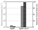
도 3은 AgNP 및 AgNP-Ga-In 사이의 전기 전도성 및 최대 스트레인의 차이를 도시하는 그래프이다.
도 4A 및 도 4B는 각자 EGaIn 처리 전 그리고 후의 전도성 잉크의 현미경 사진이다.
도 5A 및 도 5B는 도 4A 및 도 4B에 도시된 현미경 사진의 더 높은 확대율로 도시된 것으로서, 액체 금속이 어떻게 AgNP가 골재로 클러스터가 되게 야기하는지를 도시하는 현미경 사진이다.
도 6은 25μm 길이의 스캔 선(scanning line)으로 실행된 EDS 분석으로, Ag, Ga 및 In 농도 프로파일을 도시한다.
도 7은 폴리머 기판 상의 전도성 트레이스에 대한 스트레인 대 전기 저항성을 도시하는 그래프이다.
도 8은 수전사(hydrographic transfer)로 배치된 회로를 가진 3D 인쇄된 손 모형을 도시한다.
도 9는 사람 팔에 배치된, 전자 문신으로서 기능을 하는 회로를 도시한다.
도 10은 3D 인쇄된 물체에 전사된 회로를 도시한다.
도 11A 및 도 11B는 뇌 모형에 전사된 전도성 트레이스가 모형의 형태가 변형되었을 때에도 전도성을 유지하는 것을 도시한다.
Claims (20)
- 전도성 잉크를 사용하여 하나 이상의 트레이스를 포함하는 전기 회로를 기판에 인쇄하는 단계; 그리고
하나 이상의 전기 트레이스를 액체 금속으로 코팅하는 단계를 포함하고,
상기 액체 금속이 갈륨; 갈륨 및 인듐의 합금; 또는 갈륨, 인듐 및 주석의 합금인 것을 특징으로 하는 전도성 전기 트레이스를 생성하는 방법.
- 제1항에 있어서, 상기 액체 금속이 인쇄된 상기 전기 회로의 트레이스 위에 선택적으로 적층되는 것을 특징으로 하는 전도성 전기 트레이스를 생성하는 방법.
- 제2항에 있어서, 상기 선택적인 적층이 스크린 인쇄, 전기 도금, 잉크젯 인쇄 및 밀착 인화를 포함하는 군으로부터 선택되는 것을 특징으로 하는 전도성 전기 트레이스를 생성하는 방법.
- 제1항에 있어서, 상기 기판이 액체 금속으로 코팅되고, 상기 기판로부터 액체 금속을 제거하여 하나 이상의 트레이스 위에 액체 금속을 남기는 것을 더 포함하는 것을 특징으로 하는 전도성 전기 트레이스를 생성하는 방법.
- 제4항에 있어서, 액체 금속 제거 방법이 수동 닦기(manual wiping), 가스 압력 또는 유압, 초음파 세척, 산 증기, 산성 또는 염기성 액체 세척 및 전압 적용을 포함하는 군으로부터 선택되는 것을 특징으로 하는 전도성 전기 트레이스를 생성하는 방법.
- 제1항에 있어서, 상기 전도성 잉크가 은, 구리 또는 금 입자; 은, 구리 또는 금으로 덮인 입자; 또는 은, 구리 또는 금의 염을 함유하는 액체 또는 페이스트인 것을 특징으로 하는 전도성 전기 트레이스를 생성하는 방법.
- 제1항에 있어서, 상기 액체 금속이 갈륨 및 인듐의 공융(eutectic) 합금인 것을 특징으로 하는 전도성 전기 트레이스를 생성하는 방법.
- 제1항에 있어서, 상기 전기 트레이스의 인쇄가 잉크젯 인쇄, 스크린 인쇄, 롤투롤(roll-to-roll) 인쇄, 에어로졸 적층, 밀착 인화 및 스핀 코팅에 의한 균일 박막 적층으로부터 선택된 방법을 사용하여 실행되는 것을 특징으로 하는 전도성 전기 트레이스를 생성하는 방법.
- 제1항에 있어서, 상기 하나 이상의 트레이스를 액체 금속으로 코팅하는 것이 전기 전도성을 가능하게 하거나 또는 전기 전도성을 증가시키기 위해 적층된 금속 입자의 퍼콜레이션(percolation)을 가능하게 하는 것을 특징으로 하는 전도성 전기 트레이스를 생성하는 방법.
- 제1항에 있어서, 상기 하나 이상의 트레이스를 액체 금속으로 코팅하는 것이 상기 전기 회로의 기계 부하 또는 기계 스트레인에 대한 저항력을 증가시키는 것을 특징으로 하는 전도성 전기 트레이스를 생성하는 방법.
- 제1항에 있어서, 상기 기판이 폴리머 기판인 것을 특징으로 하는 전도성 전기 트레이스를 생성하는 방법.
- 제1항에 있어서, 상기 기판이 타투 전사지, 전사지 또는 수전사 용지(hydrographic paper)인 것을 특징으로 하는 전도성 전기 트레이스를 생성하는 방법.
- 제1항에 있어서, 상기 기판이 종이, 직물, 세라믹, 목재 또는 폼(foam)인 것을 특징으로 하는 전도성 전기 트레이스를 생성하는 방법.
- 제1항에 있어서, 상기 액체 금속의 적층을 위한 과정이 수동 표면 코팅, 스핀 코팅, 분무 적층, 딥 코팅, 롤투롤 코팅, 나이프 코팅 및 그라비어 코팅으로 이루어진 군으로부터 선택되는 것을 특징으로 하는 전도성 전기 트레이스를 생성하는 방법.
- 제1항에 있어서, 상기 기판이 빈 공간이 없는 한 층(full layer)의 전도성 잉크로 덮이고, 뒤이어 빈 공간이 없는 한 층의 액체 금속이 적층되고,
패터닝 방법으로 상기 전기 회로의 형태를 정의하는 것을 더 포함하는 것을 특징으로 하는 전도성 전기 트레이스를 생성하는 방법.
- 제15항에 있어서, 상기 패터닝 방법이 레이저 어블레이션 및 사진 석판술로 이루어지는 군으로부터 석택되는 것을 특징으로 하는 전도성 전기 트레이스를 생성하는 방법.
- 캐리어 매체에 현탁된 금속 입자; 및
상기 캐리어 매체에 혼합된 액체 금속을 포함하는 혼합물로서,
상기 액체 금속이 갈륨 및 인듐의 합금이고,
상기 혼합물이 상기 액체 금속의 최소 0.1 중량%인 것을 특징으로 하는 전기 전도성 패턴을 생성하기 위한 인쇄 가능한 물질.
- 제17항에 있어서, 상기 금속 입자가 은 입자 또는 은으로 코팅된 입자; 구리 입자 또는 구리로 코팅된 입자; 금 입자 또는 금으로 코팅된 입자를 포함하는 군으로부터 선택된 금속의 크기 범위가 1nm에서 1mm에 이르는 구체(spheres), 비즈(beads), 플레이크(flakes), 와이어(wires), 또는 튜브(tubes)를 포함하는 것을 특징으로 하는 인쇄 가능한 물질.
- 제17항에 있어서, 상기 캐리어 매체가 상기 인쇄 가능한 물질의 점도를 조절하기 위해 희석될 수 있는 액체 또는 폴리머인 것을 특징으로 하는 인쇄 가능한 물질.
- 제17항에 있어서, 상기 액체 금속이 초음파 혼합; 그리고 원심, 플래너터리(planetary), 및 수동 혼합을 포함하는 전단력 혼합으로 이루어진 군으로부터 선택된 방법으로 상기 캐리어 매체에 혼합될 수 있는 것을 특징으로 하는 인쇄 가능한 물질.
Applications Claiming Priority (7)
| Application Number | Priority Date | Filing Date | Title |
|---|---|---|---|
| US201762606187P | 2017-09-13 | 2017-09-13 | |
| US62/606,187 | 2017-09-13 | ||
| US201862762975P | 2018-05-25 | 2018-05-25 | |
| US62/762,975 | 2018-05-25 | ||
| PT15878218 | 2018-09-07 | ||
| PT20181000058782 | 2018-09-07 | ||
| PCT/US2018/050920 WO2019055680A1 (en) | 2017-09-13 | 2018-09-13 | LIQUID METAL FUSION WITH INKS AND CONDUCTIVE PASTES |
Publications (2)
| Publication Number | Publication Date |
|---|---|
| KR20200055009A true KR20200055009A (ko) | 2020-05-20 |
| KR102682552B1 KR102682552B1 (ko) | 2024-07-05 |
Family
ID=70919326
Family Applications (1)
| Application Number | Title | Priority Date | Filing Date |
|---|---|---|---|
| KR1020207010052A Active KR102682552B1 (ko) | 2017-09-13 | 2018-09-13 | 전도성 잉크 및 페이스트를 포함하는 액체 금속 용융물 |
Country Status (4)
| Country | Link |
|---|---|
| US (2) | US11395413B2 (ko) |
| EP (1) | EP3682717A4 (ko) |
| KR (1) | KR102682552B1 (ko) |
| WO (1) | WO2019055680A1 (ko) |
Cited By (2)
| Publication number | Priority date | Publication date | Assignee | Title |
|---|---|---|---|---|
| KR20230077363A (ko) * | 2021-11-25 | 2023-06-01 | 한국화학연구원 | 포지티브형 감광성 페이스트 조성물과, 이를 이용한 전도성 패턴이 마련된 전극 및 그 제조방법 |
| KR20240047508A (ko) | 2022-10-04 | 2024-04-12 | 광주과학기술원 | 액체 금속 나노입자-공액고분자 복합체를 포함하는 전도성 수성 잉크 및 이의 제조방법 |
Families Citing this family (21)
| Publication number | Priority date | Publication date | Assignee | Title |
|---|---|---|---|---|
| FR3067275B1 (fr) | 2017-06-07 | 2022-08-12 | Timothee Boitouzet | Procede de delignification partielle par voie supercritique ou subcritique et de remplissage d'un materiau ligno-cellulosique |
| US11212916B2 (en) * | 2018-05-08 | 2021-12-28 | W. L. Gore & Associates, Inc. | Flexible printed circuits for dermal applications |
| DE102018214367A1 (de) * | 2018-08-24 | 2020-02-27 | Karlsruher Institut für Technologie | Verfahren zur Herstellung einer elektrisch leitfähigen Verbindung auf einem Substrat, mikroelektronisches Bauelement und Verfahren zu dessen Herstellung |
| CN111849250A (zh) * | 2019-04-30 | 2020-10-30 | 北京梦之墨科技有限公司 | 一种导电墨水及电子器件 |
| US11706874B2 (en) * | 2019-08-06 | 2023-07-18 | Microsoft Technology Licensing, Llc | Electronic-circuit printing using low-cost ink |
| CN110828029A (zh) * | 2019-11-06 | 2020-02-21 | 浙江清华柔性电子技术研究院 | 导电材料及其制备方法 |
| WO2021146643A2 (en) * | 2020-01-15 | 2021-07-22 | Liquid Wire Inc. | Deposition with solid feedstock |
| KR102290112B1 (ko) * | 2020-03-18 | 2021-08-13 | 포항공과대학교 산학협력단 | 수소 도핑된 액체금속 산화물을 포함하는 전도성 액체금속 미세입자, 그를 포함하는 전도성 잉크 및 그의 제조방법 |
| US11937372B2 (en) | 2020-06-24 | 2024-03-19 | Yale University | Biphasic material and stretchable circuit board |
| FR3112449B1 (fr) | 2020-07-08 | 2022-08-26 | Sas Woodoo | Procédé de fabrication d'un dispositif électriquement conducteur en matériau ligno-cellulosique |
| CN114496447B (zh) * | 2020-10-26 | 2023-05-05 | 北京梦之墨科技有限公司 | 一种柔性射频线圈及其制备方法 |
| US11631565B2 (en) | 2020-11-10 | 2023-04-18 | Science Applications International Corporation | Thermal fuse |
| CN114574039B (zh) * | 2020-11-30 | 2023-02-10 | 北京梦之墨科技有限公司 | 一种柱形油墨及印刷用墨管 |
| US12152156B2 (en) | 2021-03-24 | 2024-11-26 | Science Applications International Corporation | Self-sintering conductive inks |
| CN113613395B (zh) * | 2021-08-11 | 2022-12-27 | 东南大学 | 一种简便高效的定制化液态金属电路图案印刷方法 |
| CN113709996B (zh) * | 2021-09-09 | 2023-10-31 | 北京星宇同辉科技有限公司 | 一种可低温下快速打印的高导电性电子电路及其制备方法和应用 |
| JP7800407B2 (ja) * | 2022-02-25 | 2026-01-16 | 株式会社村田製作所 | 電極 |
| JP2023135339A (ja) * | 2022-03-15 | 2023-09-28 | 株式会社リコー | 機能性インク、機能膜、電子部品、機能膜の形成方法、及び成膜装置 |
| CN115181453A (zh) * | 2022-06-24 | 2022-10-14 | 温州大学新材料与产业技术研究院 | 一种含镓的金属导电墨水及其制备方法和应用 |
| CN115044081B (zh) * | 2022-07-13 | 2023-10-24 | 清远高新华园科技协同创新研究院有限公司 | 一种液态金属柔性薄膜材料及其制备方法和应用 |
| CN117866484B (zh) * | 2024-03-12 | 2024-06-04 | 成都先进金属材料产业技术研究院股份有限公司 | 一种液态金属油墨及其制备方法 |
Citations (3)
| Publication number | Priority date | Publication date | Assignee | Title |
|---|---|---|---|---|
| US20160366760A1 (en) * | 2015-06-10 | 2016-12-15 | Industry Foundation Of Chonnam National University | Stretchable circuit board and method of manufacturing the same |
| JP2017039167A (ja) * | 2009-04-02 | 2017-02-23 | オーメット サーキッツ インク | 混合された合金フィラーを含む伝導性組成物 |
| US20170164461A1 (en) * | 2015-12-08 | 2017-06-08 | Intel Corporation | Conductive flexible and stretchable encapsulation method and apparatus |
Family Cites Families (8)
| Publication number | Priority date | Publication date | Assignee | Title |
|---|---|---|---|---|
| US20130202909A1 (en) * | 2012-02-06 | 2013-08-08 | Lg Chem, Ltd. | Method of producing metal nanoparticles |
| US10032538B2 (en) * | 2013-11-13 | 2018-07-24 | The United States Of America As Represented By The Secretary Of The Army | Deformable elastomeric conductors and differential electronic signal transmission |
| US9841327B2 (en) * | 2014-08-14 | 2017-12-12 | Purdue Research Foundation | Method of producing conductive patterns of nanoparticles and devices made thereof |
| WO2017072347A1 (en) * | 2015-10-30 | 2017-05-04 | Ecole Polytechnique Federale De Lausanne (Epfl) | Method for manufacturing electrical conductors, and electrical conductors manufactured according to same |
| US10672530B2 (en) * | 2016-02-29 | 2020-06-02 | Liquid Wire Inc. | Deformable conductors and related sensors, antennas and multiplexed systems |
| EP3424053B1 (en) * | 2016-02-29 | 2021-09-15 | Liquid Wire Inc. | Liquid wire |
| WO2018194517A1 (en) * | 2017-04-18 | 2018-10-25 | Nanyang Technological University | Elastic conductor, device including, and method of forming the same |
| US11057994B2 (en) * | 2017-10-03 | 2021-07-06 | Northwestern University | Conductive graphene interfacial barriers for liquid metal electronics |
-
2018
- 2018-09-13 WO PCT/US2018/050920 patent/WO2019055680A1/en not_active Ceased
- 2018-09-13 EP EP18855315.0A patent/EP3682717A4/en active Pending
- 2018-09-13 US US16/647,083 patent/US11395413B2/en active Active
- 2018-09-13 KR KR1020207010052A patent/KR102682552B1/ko active Active
-
2022
- 2022-07-05 US US17/857,356 patent/US12336115B2/en active Active
Patent Citations (3)
| Publication number | Priority date | Publication date | Assignee | Title |
|---|---|---|---|---|
| JP2017039167A (ja) * | 2009-04-02 | 2017-02-23 | オーメット サーキッツ インク | 混合された合金フィラーを含む伝導性組成物 |
| US20160366760A1 (en) * | 2015-06-10 | 2016-12-15 | Industry Foundation Of Chonnam National University | Stretchable circuit board and method of manufacturing the same |
| US20170164461A1 (en) * | 2015-12-08 | 2017-06-08 | Intel Corporation | Conductive flexible and stretchable encapsulation method and apparatus |
Cited By (2)
| Publication number | Priority date | Publication date | Assignee | Title |
|---|---|---|---|---|
| KR20230077363A (ko) * | 2021-11-25 | 2023-06-01 | 한국화학연구원 | 포지티브형 감광성 페이스트 조성물과, 이를 이용한 전도성 패턴이 마련된 전극 및 그 제조방법 |
| KR20240047508A (ko) | 2022-10-04 | 2024-04-12 | 광주과학기술원 | 액체 금속 나노입자-공액고분자 복합체를 포함하는 전도성 수성 잉크 및 이의 제조방법 |
Also Published As
| Publication number | Publication date |
|---|---|
| KR102682552B1 (ko) | 2024-07-05 |
| EP3682717A4 (en) | 2021-06-23 |
| US11395413B2 (en) | 2022-07-19 |
| US12336115B2 (en) | 2025-06-17 |
| EP3682717A1 (en) | 2020-07-22 |
| US20200221580A1 (en) | 2020-07-09 |
| US20220346238A1 (en) | 2022-10-27 |
| WO2019055680A1 (en) | 2019-03-21 |
Similar Documents
| Publication | Publication Date | Title |
|---|---|---|
| US12336115B2 (en) | Liquid metal fusion with conductive inks and pastes | |
| Lopes et al. | Hydroprinted electronics: ultrathin stretchable Ag–In–Ga E-skin for bioelectronics and human–machine interaction | |
| Li et al. | Recent advancement of emerging nano copper-based printable flexible hybrid electronics | |
| Lu et al. | Room‐temperature liquid metals for flexible electronic devices | |
| Huang et al. | Patterning of metal nanowire networks: methods and applications | |
| Xiao et al. | Scalable strategy to directly prepare 2D and 3D liquid metal circuits based on laser-induced selective metallization | |
| TWI682405B (zh) | 導電性銀糊劑 | |
| Al-Milaji et al. | Direct embedment and alignment of silver nanowires by inkjet printing for stretchable conductors | |
| Wu et al. | Buckle-delamination-enabled stretchable silver nanowire conductors | |
| US20160168715A1 (en) | Electroless copper plating polydopamine nanoparticles | |
| Lee et al. | The development and investigation of highly stretchable conductive inks for 3-dimensional printed in-mold electronics | |
| JP6690528B2 (ja) | 導電性膜 | |
| Shukla et al. | Surface embedded metal nanowire–liquid metal–elastomer hybrid composites for stretchable electronics | |
| Zu et al. | Enhancing electrical conductivity of stretchable liquid metal–silver composites through direct ink writing | |
| Yang et al. | Fabrication of flexible microheater with tunable heating capabilities by direct laser writing and selective electrodeposition | |
| Ren et al. | Laser direct activation of polyimide for selective electroless plating of flexible conductive patterns | |
| EP4010197B1 (en) | Electronic-circuit printing using low-cost ink | |
| Tan et al. | Fabrication approaches of soft electronics | |
| Li et al. | Supermetallophobic functional coatings based on silicate clays and a method to pattern liquid metals | |
| Tetik et al. | Highly conductive laser-induced graphene through the deposition of liquid metal particles for flexible electronics | |
| TWI648751B (zh) | 在彈性基材上之透明導電塗層 | |
| Ji et al. | Laser patterning of highly conductive flexible circuits | |
| Kim et al. | High-quality microprintable and stretchable conductors for high-performance 5G wireless communication | |
| WO2020161077A1 (en) | Method of manufacturing an elastic conductor, elastic conductor and electronic device comprising the elastic conductor | |
| Rahman et al. | Direct writing of stretchable metal flake conductors: improved stretchability and conductivity by combining differently sintered materials |
Legal Events
| Date | Code | Title | Description |
|---|---|---|---|
| PA0105 | International application |
Patent event date: 20200407 Patent event code: PA01051R01D Comment text: International Patent Application |
|
| PG1501 | Laying open of application | ||
| A201 | Request for examination | ||
| PA0201 | Request for examination |
Patent event code: PA02012R01D Patent event date: 20210901 Comment text: Request for Examination of Application |
|
| E902 | Notification of reason for refusal | ||
| PE0902 | Notice of grounds for rejection |
Comment text: Notification of reason for refusal Patent event date: 20221124 Patent event code: PE09021S01D |
|
| E902 | Notification of reason for refusal | ||
| PE0902 | Notice of grounds for rejection |
Comment text: Notification of reason for refusal Patent event date: 20230720 Patent event code: PE09021S01D |
|
| E701 | Decision to grant or registration of patent right | ||
| PE0701 | Decision of registration |
Patent event code: PE07011S01D Comment text: Decision to Grant Registration Patent event date: 20240416 |
|
| PR0701 | Registration of establishment |
Comment text: Registration of Establishment Patent event date: 20240703 Patent event code: PR07011E01D |
|
| PR1002 | Payment of registration fee |
Payment date: 20240703 End annual number: 3 Start annual number: 1 |
|
| PG1601 | Publication of registration |