KR20200056310A - 광 조사 장치 - Google Patents
광 조사 장치 Download PDFInfo
- Publication number
- KR20200056310A KR20200056310A KR1020190142536A KR20190142536A KR20200056310A KR 20200056310 A KR20200056310 A KR 20200056310A KR 1020190142536 A KR1020190142536 A KR 1020190142536A KR 20190142536 A KR20190142536 A KR 20190142536A KR 20200056310 A KR20200056310 A KR 20200056310A
- Authority
- KR
- South Korea
- Prior art keywords
- module
- connector
- heat transfer
- light source
- unit
- Prior art date
- Legal status (The legal status is an assumption and is not a legal conclusion. Google has not performed a legal analysis and makes no representation as to the accuracy of the status listed.)
- Granted
Links
Images

Classifications
-
- G—PHYSICS
- G03—PHOTOGRAPHY; CINEMATOGRAPHY; ANALOGOUS TECHNIQUES USING WAVES OTHER THAN OPTICAL WAVES; ELECTROGRAPHY; HOLOGRAPHY
- G03F—PHOTOMECHANICAL PRODUCTION OF TEXTURED OR PATTERNED SURFACES, e.g. FOR PRINTING, FOR PROCESSING OF SEMICONDUCTOR DEVICES; MATERIALS THEREFOR; ORIGINALS THEREFOR; APPARATUS SPECIALLY ADAPTED THEREFOR
- G03F7/00—Photomechanical, e.g. photolithographic, production of textured or patterned surfaces, e.g. printing surfaces; Materials therefor, e.g. comprising photoresists; Apparatus specially adapted therefor
- G03F7/20—Exposure; Apparatus therefor
- G03F7/2002—Exposure; Apparatus therefor with visible light or UV light, through an original having an opaque pattern on a transparent support, e.g. film printing, projection printing; by reflection of visible or UV light from an original such as a printed image
- G03F7/2008—Exposure; Apparatus therefor with visible light or UV light, through an original having an opaque pattern on a transparent support, e.g. film printing, projection printing; by reflection of visible or UV light from an original such as a printed image characterised by the reflectors, diffusers, light or heat filtering means or anti-reflective means used
-
- G—PHYSICS
- G03—PHOTOGRAPHY; CINEMATOGRAPHY; ANALOGOUS TECHNIQUES USING WAVES OTHER THAN OPTICAL WAVES; ELECTROGRAPHY; HOLOGRAPHY
- G03F—PHOTOMECHANICAL PRODUCTION OF TEXTURED OR PATTERNED SURFACES, e.g. FOR PRINTING, FOR PROCESSING OF SEMICONDUCTOR DEVICES; MATERIALS THEREFOR; ORIGINALS THEREFOR; APPARATUS SPECIALLY ADAPTED THEREFOR
- G03F7/00—Photomechanical, e.g. photolithographic, production of textured or patterned surfaces, e.g. printing surfaces; Materials therefor, e.g. comprising photoresists; Apparatus specially adapted therefor
- G03F7/20—Exposure; Apparatus therefor
- G03F7/2022—Multi-step exposure, e.g. hybrid; backside exposure; blanket exposure, e.g. for image reversal; edge exposure, e.g. for edge bead removal; corrective exposure
-
- G—PHYSICS
- G03—PHOTOGRAPHY; CINEMATOGRAPHY; ANALOGOUS TECHNIQUES USING WAVES OTHER THAN OPTICAL WAVES; ELECTROGRAPHY; HOLOGRAPHY
- G03F—PHOTOMECHANICAL PRODUCTION OF TEXTURED OR PATTERNED SURFACES, e.g. FOR PRINTING, FOR PROCESSING OF SEMICONDUCTOR DEVICES; MATERIALS THEREFOR; ORIGINALS THEREFOR; APPARATUS SPECIALLY ADAPTED THEREFOR
- G03F7/00—Photomechanical, e.g. photolithographic, production of textured or patterned surfaces, e.g. printing surfaces; Materials therefor, e.g. comprising photoresists; Apparatus specially adapted therefor
- G03F7/20—Exposure; Apparatus therefor
-
- G—PHYSICS
- G03—PHOTOGRAPHY; CINEMATOGRAPHY; ANALOGOUS TECHNIQUES USING WAVES OTHER THAN OPTICAL WAVES; ELECTROGRAPHY; HOLOGRAPHY
- G03F—PHOTOMECHANICAL PRODUCTION OF TEXTURED OR PATTERNED SURFACES, e.g. FOR PRINTING, FOR PROCESSING OF SEMICONDUCTOR DEVICES; MATERIALS THEREFOR; ORIGINALS THEREFOR; APPARATUS SPECIALLY ADAPTED THEREFOR
- G03F7/00—Photomechanical, e.g. photolithographic, production of textured or patterned surfaces, e.g. printing surfaces; Materials therefor, e.g. comprising photoresists; Apparatus specially adapted therefor
- G03F7/20—Exposure; Apparatus therefor
- G03F7/2002—Exposure; Apparatus therefor with visible light or UV light, through an original having an opaque pattern on a transparent support, e.g. film printing, projection printing; by reflection of visible or UV light from an original such as a printed image
-
- G—PHYSICS
- G03—PHOTOGRAPHY; CINEMATOGRAPHY; ANALOGOUS TECHNIQUES USING WAVES OTHER THAN OPTICAL WAVES; ELECTROGRAPHY; HOLOGRAPHY
- G03F—PHOTOMECHANICAL PRODUCTION OF TEXTURED OR PATTERNED SURFACES, e.g. FOR PRINTING, FOR PROCESSING OF SEMICONDUCTOR DEVICES; MATERIALS THEREFOR; ORIGINALS THEREFOR; APPARATUS SPECIALLY ADAPTED THEREFOR
- G03F7/00—Photomechanical, e.g. photolithographic, production of textured or patterned surfaces, e.g. printing surfaces; Materials therefor, e.g. comprising photoresists; Apparatus specially adapted therefor
- G03F7/16—Coating processes; Apparatus therefor
- G03F7/168—Finishing the coated layer, e.g. drying, baking, soaking
-
- G—PHYSICS
- G03—PHOTOGRAPHY; CINEMATOGRAPHY; ANALOGOUS TECHNIQUES USING WAVES OTHER THAN OPTICAL WAVES; ELECTROGRAPHY; HOLOGRAPHY
- G03F—PHOTOMECHANICAL PRODUCTION OF TEXTURED OR PATTERNED SURFACES, e.g. FOR PRINTING, FOR PROCESSING OF SEMICONDUCTOR DEVICES; MATERIALS THEREFOR; ORIGINALS THEREFOR; APPARATUS SPECIALLY ADAPTED THEREFOR
- G03F7/00—Photomechanical, e.g. photolithographic, production of textured or patterned surfaces, e.g. printing surfaces; Materials therefor, e.g. comprising photoresists; Apparatus specially adapted therefor
- G03F7/20—Exposure; Apparatus therefor
- G03F7/2002—Exposure; Apparatus therefor with visible light or UV light, through an original having an opaque pattern on a transparent support, e.g. film printing, projection printing; by reflection of visible or UV light from an original such as a printed image
- G03F7/2014—Contact or film exposure of light sensitive plates such as lithographic plates or circuit boards, e.g. in a vacuum frame
- G03F7/2016—Contact mask being integral part of the photosensitive element and subject to destructive removal during post-exposure processing
- G03F7/202—Masking pattern being obtained by thermal means, e.g. laser ablation
-
- G—PHYSICS
- G03—PHOTOGRAPHY; CINEMATOGRAPHY; ANALOGOUS TECHNIQUES USING WAVES OTHER THAN OPTICAL WAVES; ELECTROGRAPHY; HOLOGRAPHY
- G03F—PHOTOMECHANICAL PRODUCTION OF TEXTURED OR PATTERNED SURFACES, e.g. FOR PRINTING, FOR PROCESSING OF SEMICONDUCTOR DEVICES; MATERIALS THEREFOR; ORIGINALS THEREFOR; APPARATUS SPECIALLY ADAPTED THEREFOR
- G03F7/00—Photomechanical, e.g. photolithographic, production of textured or patterned surfaces, e.g. printing surfaces; Materials therefor, e.g. comprising photoresists; Apparatus specially adapted therefor
- G03F7/20—Exposure; Apparatus therefor
- G03F7/2041—Exposure; Apparatus therefor in the presence of a fluid, e.g. immersion; using fluid cooling means
-
- G—PHYSICS
- G03—PHOTOGRAPHY; CINEMATOGRAPHY; ANALOGOUS TECHNIQUES USING WAVES OTHER THAN OPTICAL WAVES; ELECTROGRAPHY; HOLOGRAPHY
- G03F—PHOTOMECHANICAL PRODUCTION OF TEXTURED OR PATTERNED SURFACES, e.g. FOR PRINTING, FOR PROCESSING OF SEMICONDUCTOR DEVICES; MATERIALS THEREFOR; ORIGINALS THEREFOR; APPARATUS SPECIALLY ADAPTED THEREFOR
- G03F7/00—Photomechanical, e.g. photolithographic, production of textured or patterned surfaces, e.g. printing surfaces; Materials therefor, e.g. comprising photoresists; Apparatus specially adapted therefor
- G03F7/70—Microphotolithographic exposure; Apparatus therefor
- G03F7/70008—Production of exposure light, i.e. light sources
-
- G—PHYSICS
- G03—PHOTOGRAPHY; CINEMATOGRAPHY; ANALOGOUS TECHNIQUES USING WAVES OTHER THAN OPTICAL WAVES; ELECTROGRAPHY; HOLOGRAPHY
- G03F—PHOTOMECHANICAL PRODUCTION OF TEXTURED OR PATTERNED SURFACES, e.g. FOR PRINTING, FOR PROCESSING OF SEMICONDUCTOR DEVICES; MATERIALS THEREFOR; ORIGINALS THEREFOR; APPARATUS SPECIALLY ADAPTED THEREFOR
- G03F7/00—Photomechanical, e.g. photolithographic, production of textured or patterned surfaces, e.g. printing surfaces; Materials therefor, e.g. comprising photoresists; Apparatus specially adapted therefor
- G03F7/70—Microphotolithographic exposure; Apparatus therefor
- G03F7/708—Construction of apparatus, e.g. environment aspects, hygiene aspects or materials
- G03F7/70858—Environment aspects, e.g. pressure of beam-path gas, temperature
- G03F7/70883—Environment aspects, e.g. pressure of beam-path gas, temperature of optical system
- G03F7/70891—Temperature
-
- H—ELECTRICITY
- H10—SEMICONDUCTOR DEVICES; ELECTRIC SOLID-STATE DEVICES NOT OTHERWISE PROVIDED FOR
- H10N—ELECTRIC SOLID-STATE DEVICES NOT OTHERWISE PROVIDED FOR
- H10N10/00—Thermoelectric devices comprising a junction of dissimilar materials, i.e. devices exhibiting Seebeck or Peltier effects
- H10N10/10—Thermoelectric devices comprising a junction of dissimilar materials, i.e. devices exhibiting Seebeck or Peltier effects operating with only the Peltier or Seebeck effects
-
- G—PHYSICS
- G03—PHOTOGRAPHY; CINEMATOGRAPHY; ANALOGOUS TECHNIQUES USING WAVES OTHER THAN OPTICAL WAVES; ELECTROGRAPHY; HOLOGRAPHY
- G03F—PHOTOMECHANICAL PRODUCTION OF TEXTURED OR PATTERNED SURFACES, e.g. FOR PRINTING, FOR PROCESSING OF SEMICONDUCTOR DEVICES; MATERIALS THEREFOR; ORIGINALS THEREFOR; APPARATUS SPECIALLY ADAPTED THEREFOR
- G03F7/00—Photomechanical, e.g. photolithographic, production of textured or patterned surfaces, e.g. printing surfaces; Materials therefor, e.g. comprising photoresists; Apparatus specially adapted therefor
- G03F7/70—Microphotolithographic exposure; Apparatus therefor
- G03F7/70216—Mask projection systems
- G03F7/70341—Details of immersion lithography aspects, e.g. exposure media or control of immersion liquid supply
Landscapes
- Physics & Mathematics (AREA)
- General Physics & Mathematics (AREA)
- Health & Medical Sciences (AREA)
- Life Sciences & Earth Sciences (AREA)
- Atmospheric Sciences (AREA)
- Toxicology (AREA)
- Engineering & Computer Science (AREA)
- Environmental & Geological Engineering (AREA)
- Epidemiology (AREA)
- Public Health (AREA)
- Optics & Photonics (AREA)
- Exposure And Positioning Against Photoresist Photosensitive Materials (AREA)
- Heating, Cooling, Or Curing Plastics Or The Like In General (AREA)
- Steering Control In Accordance With Driving Conditions (AREA)
- Exposure Of Semiconductors, Excluding Electron Or Ion Beam Exposure (AREA)
Abstract
Description
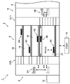
도 2는 도 1의 II-II선 단면도이다.
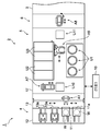
도 3은 처리 모듈(BCT 모듈, HMCT 모듈 및 COT 모듈)을 나타내는 상면도이다.
도 4는 처리 모듈(DEV 모듈)을 나타내는 상면도이다.
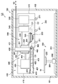
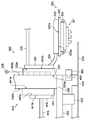
도 5는 광 조사 장치의 일례를 나타내는 단면도이다.
도 6은 광원 모듈의 근방을 나타내는 단면도이다.
Claims (7)
- 기판을 유지하도록 구성된 기판 유지부와,
광 조사 유닛과,
급전 유닛을 구비하고,
상기 광 조사 유닛은,
상기 기판의 표면에 광을 조사하도록 구성된 광원과,
상기 광원에 대하여 전기적으로 접속된 제 1 커넥터를 포함하고,
상기 급전 유닛은,
상기 광원에 전력을 공급하도록 구성된 전원 모듈과,
상기 전원 모듈에 대하여 전기적으로 접속되어 있고, 상기 제 1 커넥터와 착탈 가능하게 구성된 제 2 커넥터를 포함하고,
상기 광 조사 유닛과 상기 급전 유닛은, 상기 제 1 커넥터와 상기 제 2 커넥터가 결합됨으로써 일체화되고, 상기 제 1 커넥터와 상기 제 2 커넥터와의 결합이 해제됨으로써 개개로 분리되는, 광 조사 장치. - 제 1 항에 있어서,
상기 광 조사 유닛은, 상기 광원에 대하여 열적으로 접속된 전열 모듈을 더 포함하고,
상기 급전 유닛은 냉각 모듈을 더 포함하고,
상기 제 1 커넥터와 상기 제 2 커넥터와의 결합에 의해 상기 광 조사 유닛과 상기 급전 유닛이 일체화된 상태에 있어서, 상기 냉각 모듈은 상기 전열 모듈과 접촉하고, 상기 전열 모듈을 개재하여 상기 광원을 냉각하도록 구성되어 있는, 장치. - 제 2 항에 있어서,
상기 전열 모듈은, 상기 광 조사 유닛의 외부에 노출되는 제 1 접촉면을 포함하고,
상기 냉각 모듈은, 상기 급전 유닛의 외부에 노출되는 제 2 접촉면을 포함하고,
상기 제 1 커넥터와 상기 제 2 커넥터와의 결합에 의해 상기 광 조사 유닛과 상기 급전 유닛이 일체화된 상태에 있어서, 상기 전열 모듈의 상기 제 1 접촉면과 상기 냉각 모듈의 상기 제 2 접촉면이 접촉하는, 장치. - 제 2 항 또는 제 3 항에 있어서,
상기 전열 모듈은 상기 냉각 모듈에 대하여 흡착 가능하게 구성되어 있는, 장치. - 제 2 항 또는 제 3 항에 있어서,
상기 냉각 모듈은 수냉식의 열 교환기인, 장치. - 제 2 항 또는 제 3 항에 있어서,
상기 광 조사 유닛은 펠티에 소자를 더 포함하고,
상기 펠티에 소자의 냉각부는 상기 광원과 열적으로 접속되어 있고,
상기 펠티에 소자의 발열부는 상기 전열 모듈과 열적으로 접속되어 있는, 장치. - 제 2 항 또는 제 3 항에 있어서,
상기 전열 모듈 및 상기 냉각 모듈 중 적어도 일방을 타방을 향해 외방으로 힘을 가하도록 구성된 부세 부재를 더 구비하는, 장치.
Applications Claiming Priority (2)
| Application Number | Priority Date | Filing Date | Title |
|---|---|---|---|
| JPJP-P-2018-213809 | 2018-11-14 | ||
| JP2018213809A JP7178240B2 (ja) | 2018-11-14 | 2018-11-14 | 光照射装置 |
Publications (2)
| Publication Number | Publication Date |
|---|---|
| KR20200056310A true KR20200056310A (ko) | 2020-05-22 |
| KR102805864B1 KR102805864B1 (ko) | 2025-05-14 |
Family
ID=70551386
Family Applications (1)
| Application Number | Title | Priority Date | Filing Date |
|---|---|---|---|
| KR1020190142536A Active KR102805864B1 (ko) | 2018-11-14 | 2019-11-08 | 광 조사 장치 |
Country Status (5)
| Country | Link |
|---|---|
| US (1) | US10877376B2 (ko) |
| JP (1) | JP7178240B2 (ko) |
| KR (1) | KR102805864B1 (ko) |
| CN (1) | CN111190329B (ko) |
| TW (1) | TWI811476B (ko) |
Families Citing this family (1)
| Publication number | Priority date | Publication date | Assignee | Title |
|---|---|---|---|---|
| KR102740948B1 (ko) | 2021-12-28 | 2024-12-11 | 세메스 주식회사 | 조사 모듈 및 이를 포함하는 기판 처리 장치 |
Citations (5)
| Publication number | Priority date | Publication date | Assignee | Title |
|---|---|---|---|---|
| JPH09102455A (ja) * | 1995-10-05 | 1997-04-15 | Dainippon Screen Mfg Co Ltd | 基板の周辺部露光装置 |
| JP2008102372A (ja) * | 2006-10-19 | 2008-05-01 | Sanyo Electric Co Ltd | 電源冷却機構及びそれを用いた投写型映像表示装置 |
| US20100044589A1 (en) * | 2008-08-19 | 2010-02-25 | Spectronics Corporation | Modular lamp head and assembly for non-destructive testing |
| US20100118287A1 (en) * | 2007-04-12 | 2010-05-13 | Takayuki Kikuchi | Discharge lamp, connecting cable, light source apparatus, and exposure apparatus |
| JP2018084804A (ja) | 2016-11-17 | 2018-05-31 | 東京エレクトロン株式会社 | 露光装置、露光装置の調整方法及び記憶媒体 |
Family Cites Families (9)
| Publication number | Priority date | Publication date | Assignee | Title |
|---|---|---|---|---|
| JP4495019B2 (ja) * | 2005-03-28 | 2010-06-30 | 東レエンジニアリング株式会社 | 周辺露光装置 |
| JP4577064B2 (ja) * | 2005-03-30 | 2010-11-10 | ウシオ電機株式会社 | 光照射装置および光照射装置における光源ユニットの交換方法 |
| JP4400547B2 (ja) * | 2005-10-28 | 2010-01-20 | ウシオ電機株式会社 | エキシマランプ及びエキシマランプを搭載した紫外線照射装置 |
| CN101548133B (zh) * | 2007-04-12 | 2014-03-12 | 株式会社尼康 | 放电灯、连接用线缆、光源装置及曝光装置 |
| WO2010121844A1 (en) * | 2009-04-20 | 2010-10-28 | Asml Netherlands B.V. | Lithographic projection apparatus and device manufacturing method |
| JP2016111268A (ja) * | 2014-12-09 | 2016-06-20 | キヤノン株式会社 | 冷却装置、照明光学系、露光装置、並びに物品の製造方法 |
| KR20180091052A (ko) * | 2015-12-09 | 2018-08-14 | 가부시키가이샤 니콘 | 방전 램프 및 그 교환 방법, 그리고 노광 방법 및 장치 |
| KR102222776B1 (ko) * | 2017-01-24 | 2021-03-05 | 가부시키가이샤 에바라 세이사꾸쇼 | 도금 장치, 도금 방법, 기판 홀더, 저항 측정 모듈, 및 기판 홀더를 검사하는 방법 |
| JP6844292B2 (ja) * | 2017-02-09 | 2021-03-17 | ウシオ電機株式会社 | 光照射器および光照射装置 |
-
2018
- 2018-11-14 JP JP2018213809A patent/JP7178240B2/ja active Active
-
2019
- 2019-11-05 TW TW108140010A patent/TWI811476B/zh active
- 2019-11-08 KR KR1020190142536A patent/KR102805864B1/ko active Active
- 2019-11-12 US US16/680,650 patent/US10877376B2/en active Active
- 2019-11-12 CN CN201911099918.5A patent/CN111190329B/zh active Active
Patent Citations (5)
| Publication number | Priority date | Publication date | Assignee | Title |
|---|---|---|---|---|
| JPH09102455A (ja) * | 1995-10-05 | 1997-04-15 | Dainippon Screen Mfg Co Ltd | 基板の周辺部露光装置 |
| JP2008102372A (ja) * | 2006-10-19 | 2008-05-01 | Sanyo Electric Co Ltd | 電源冷却機構及びそれを用いた投写型映像表示装置 |
| US20100118287A1 (en) * | 2007-04-12 | 2010-05-13 | Takayuki Kikuchi | Discharge lamp, connecting cable, light source apparatus, and exposure apparatus |
| US20100044589A1 (en) * | 2008-08-19 | 2010-02-25 | Spectronics Corporation | Modular lamp head and assembly for non-destructive testing |
| JP2018084804A (ja) | 2016-11-17 | 2018-05-31 | 東京エレクトロン株式会社 | 露光装置、露光装置の調整方法及び記憶媒体 |
Also Published As
| Publication number | Publication date |
|---|---|
| US10877376B2 (en) | 2020-12-29 |
| US20200150537A1 (en) | 2020-05-14 |
| JP7178240B2 (ja) | 2022-11-25 |
| CN111190329B (zh) | 2024-07-09 |
| TW202024807A (zh) | 2020-07-01 |
| TWI811476B (zh) | 2023-08-11 |
| KR102805864B1 (ko) | 2025-05-14 |
| CN111190329A (zh) | 2020-05-22 |
| JP2020079896A (ja) | 2020-05-28 |
Similar Documents
| Publication | Publication Date | Title |
|---|---|---|
| US8973495B2 (en) | Imprint apparatus, imprint method, and article manufacturing method | |
| KR101922260B1 (ko) | 노광 장치, 기판 처리 장치, 기판의 노광 방법 및 기판 처리 방법 | |
| KR102624099B1 (ko) | 열처리 장치, 열판의 냉각 방법 및 컴퓨터 판독 가능한 기록 매체 | |
| US20120086142A1 (en) | Imprint system, imprint method, and non-transitory computer storage medium | |
| KR20160017699A (ko) | 베이크 유닛, 이를 포함하는 기판 처리 장치 및 방법 | |
| TW201202841A (en) | Light processing apparatus and light processing method | |
| KR20200056310A (ko) | 광 조사 장치 | |
| KR20170052333A (ko) | 냉각 유닛, 기판 처리 장치, 그리고 기판 처리 방법 | |
| JP3259226B2 (ja) | 熱処理方法及び熱処理装置 | |
| WO2010150740A1 (ja) | テンプレート処理装置、インプリントシステム、テンプレート処理方法及びコンピュータ記憶媒体 | |
| KR100818019B1 (ko) | 기판처리장치 및 기판처리방법 | |
| JP5749613B2 (ja) | 基板処理装置 | |
| JP2854716B2 (ja) | 露光装置 | |
| JP3259227B2 (ja) | 熱処理方法及び熱処理装置 | |
| JP2016213438A (ja) | 基板処理方法、基板処理装置及び基板処理システム | |
| KR102296277B1 (ko) | 기판 처리 장치 | |
| US12298676B2 (en) | Substrate processing apparatus | |
| KR102492396B1 (ko) | 기판 처리 방법, 기판 처리 장치 및 기판 처리 시스템 | |
| JP5352433B2 (ja) | 露光装置 | |
| KR101495284B1 (ko) | 반송 유닛 및 반송 유닛의 제어방법, 그리고 이를 이용한 기판 처리 장치 및 방법 | |
| JP6537456B2 (ja) | 熱処理装置、熱処理方法及びコンピュータ読み取り可能な記録媒体 | |
| KR102385847B1 (ko) | 기판 처리 장치 및 기판 처리 방법 | |
| KR20230101660A (ko) | 기판 반송 장치 및 이를 가지는 기판 처리 설비 | |
| JPH0878388A (ja) | 表面処理装置 | |
| KR20210021184A (ko) | 기판 처리 설비 |
Legal Events
| Date | Code | Title | Description |
|---|---|---|---|
| PA0109 | Patent application |
Patent event code: PA01091R01D Comment text: Patent Application Patent event date: 20191108 |
|
| PG1501 | Laying open of application | ||
| A201 | Request for examination | ||
| PA0201 | Request for examination |
Patent event code: PA02012R01D Patent event date: 20220810 Comment text: Request for Examination of Application Patent event code: PA02011R01I Patent event date: 20191108 Comment text: Patent Application |
|
| E902 | Notification of reason for refusal | ||
| PE0902 | Notice of grounds for rejection |
Comment text: Notification of reason for refusal Patent event date: 20240607 Patent event code: PE09021S01D |
|
| E701 | Decision to grant or registration of patent right | ||
| PE0701 | Decision of registration |
Patent event code: PE07011S01D Comment text: Decision to Grant Registration Patent event date: 20250206 |
|
| PG1601 | Publication of registration |