KR20200057372A - 도핑된 주석 산화물 박막 트랜지스터 및 그 제조 방법 - Google Patents
도핑된 주석 산화물 박막 트랜지스터 및 그 제조 방법 Download PDFInfo
- Publication number
- KR20200057372A KR20200057372A KR1020180141672A KR20180141672A KR20200057372A KR 20200057372 A KR20200057372 A KR 20200057372A KR 1020180141672 A KR1020180141672 A KR 1020180141672A KR 20180141672 A KR20180141672 A KR 20180141672A KR 20200057372 A KR20200057372 A KR 20200057372A
- Authority
- KR
- South Korea
- Prior art keywords
- thin film
- film transistor
- channel layer
- tin oxide
- tin
- Prior art date
- Legal status (The legal status is an assumption and is not a legal conclusion. Google has not performed a legal analysis and makes no representation as to the accuracy of the status listed.)
- Granted
Links
Images





Classifications
-
- H—ELECTRICITY
- H10—SEMICONDUCTOR DEVICES; ELECTRIC SOLID-STATE DEVICES NOT OTHERWISE PROVIDED FOR
- H10D—INORGANIC ELECTRIC SEMICONDUCTOR DEVICES
- H10D30/00—Field-effect transistors [FET]
- H10D30/60—Insulated-gate field-effect transistors [IGFET]
- H10D30/67—Thin-film transistors [TFT]
- H10D30/674—Thin-film transistors [TFT] characterised by the active materials
- H10D30/6755—Oxide semiconductors, e.g. zinc oxide, copper aluminium oxide or cadmium stannate
-
- H01L29/7869—
-
- H01L21/0228—
-
- H01L21/324—
-
- H01L29/66742—
-
- H01L29/78606—
-
- H01L29/78618—
-
- H01L29/78696—
-
- H—ELECTRICITY
- H10—SEMICONDUCTOR DEVICES; ELECTRIC SOLID-STATE DEVICES NOT OTHERWISE PROVIDED FOR
- H10D—INORGANIC ELECTRIC SEMICONDUCTOR DEVICES
- H10D30/00—Field-effect transistors [FET]
- H10D30/01—Manufacture or treatment
- H10D30/021—Manufacture or treatment of FETs having insulated gates [IGFET]
- H10D30/031—Manufacture or treatment of FETs having insulated gates [IGFET] of thin-film transistors [TFT]
-
- H—ELECTRICITY
- H10—SEMICONDUCTOR DEVICES; ELECTRIC SOLID-STATE DEVICES NOT OTHERWISE PROVIDED FOR
- H10D—INORGANIC ELECTRIC SEMICONDUCTOR DEVICES
- H10D30/00—Field-effect transistors [FET]
- H10D30/60—Insulated-gate field-effect transistors [IGFET]
- H10D30/67—Thin-film transistors [TFT]
-
- H—ELECTRICITY
- H10—SEMICONDUCTOR DEVICES; ELECTRIC SOLID-STATE DEVICES NOT OTHERWISE PROVIDED FOR
- H10D—INORGANIC ELECTRIC SEMICONDUCTOR DEVICES
- H10D30/00—Field-effect transistors [FET]
- H10D30/60—Insulated-gate field-effect transistors [IGFET]
- H10D30/67—Thin-film transistors [TFT]
- H10D30/6704—Thin-film transistors [TFT] having supplementary regions or layers in the thin films or in the insulated bulk substrates for controlling properties of the device
-
- H—ELECTRICITY
- H10—SEMICONDUCTOR DEVICES; ELECTRIC SOLID-STATE DEVICES NOT OTHERWISE PROVIDED FOR
- H10D—INORGANIC ELECTRIC SEMICONDUCTOR DEVICES
- H10D30/00—Field-effect transistors [FET]
- H10D30/60—Insulated-gate field-effect transistors [IGFET]
- H10D30/67—Thin-film transistors [TFT]
- H10D30/6704—Thin-film transistors [TFT] having supplementary regions or layers in the thin films or in the insulated bulk substrates for controlling properties of the device
- H10D30/6713—Thin-film transistors [TFT] having supplementary regions or layers in the thin films or in the insulated bulk substrates for controlling properties of the device characterised by the properties of the source or drain regions, e.g. compositions or sectional shapes
-
- H—ELECTRICITY
- H10—SEMICONDUCTOR DEVICES; ELECTRIC SOLID-STATE DEVICES NOT OTHERWISE PROVIDED FOR
- H10D—INORGANIC ELECTRIC SEMICONDUCTOR DEVICES
- H10D30/00—Field-effect transistors [FET]
- H10D30/60—Insulated-gate field-effect transistors [IGFET]
- H10D30/67—Thin-film transistors [TFT]
- H10D30/6757—Thin-film transistors [TFT] characterised by the structure of the channel, e.g. transverse or longitudinal shape or doping profile
-
- H—ELECTRICITY
- H10—SEMICONDUCTOR DEVICES; ELECTRIC SOLID-STATE DEVICES NOT OTHERWISE PROVIDED FOR
- H10D—INORGANIC ELECTRIC SEMICONDUCTOR DEVICES
- H10D48/00—Individual devices not covered by groups H10D1/00 - H10D44/00
- H10D48/30—Devices controlled by electric currents or voltages
-
- H—ELECTRICITY
- H10—SEMICONDUCTOR DEVICES; ELECTRIC SOLID-STATE DEVICES NOT OTHERWISE PROVIDED FOR
- H10P—GENERIC PROCESSES OR APPARATUS FOR THE MANUFACTURE OR TREATMENT OF DEVICES COVERED BY CLASS H10
- H10P14/00—Formation of materials, e.g. in the shape of layers or pillars
- H10P14/60—Formation of materials, e.g. in the shape of layers or pillars of insulating materials
- H10P14/63—Formation of materials, e.g. in the shape of layers or pillars of insulating materials characterised by the formation processes
- H10P14/6326—Deposition processes
- H10P14/6328—Deposition from the gas or vapour phase
- H10P14/6334—Deposition from the gas or vapour phase using decomposition or reaction of gaseous or vapour phase compounds, i.e. chemical vapour deposition
- H10P14/6339—Deposition from the gas or vapour phase using decomposition or reaction of gaseous or vapour phase compounds, i.e. chemical vapour deposition deposition by cyclic CVD, e.g. ALD, ALE or pulsed CVD
-
- H—ELECTRICITY
- H10—SEMICONDUCTOR DEVICES; ELECTRIC SOLID-STATE DEVICES NOT OTHERWISE PROVIDED FOR
- H10P—GENERIC PROCESSES OR APPARATUS FOR THE MANUFACTURE OR TREATMENT OF DEVICES COVERED BY CLASS H10
- H10P95/00—Generic processes or apparatus for manufacture or treatments not covered by the other groups of this subclass
-
- H—ELECTRICITY
- H10—SEMICONDUCTOR DEVICES; ELECTRIC SOLID-STATE DEVICES NOT OTHERWISE PROVIDED FOR
- H10P—GENERIC PROCESSES OR APPARATUS FOR THE MANUFACTURE OR TREATMENT OF DEVICES COVERED BY CLASS H10
- H10P95/00—Generic processes or apparatus for manufacture or treatments not covered by the other groups of this subclass
- H10P95/90—Thermal treatments, e.g. annealing or sintering
Landscapes
- Thin Film Transistor (AREA)
Abstract
Description
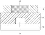
도 2는 본 발명의 일시예에 따른 도핑된 채널층을 포함하는 하부 게이트(bottom gate) 코-플래너(co-planar) 구조의 박막 트랜지스터의 단면도이다.
도 3은 본 발명의 하부 게이트(bottom gate) 코-플래너(co-planar) 구조의 박막 트랜지스터의 제조 공정의 모식도이다.
도 4는 본 발명의 일 실시예에 따른 도핑된 채널층을 형성하는 제조 공정의 모식도이다.
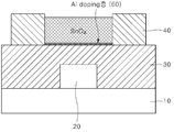
도 5는 본 발명의 비교예에 따른 도핑된 채널층을 포함하는 하부 게이트(bottom gate) 코-플래너(co-planar) 구조의 박막 트랜지스터의 단면도이다.
도 6은 본 발명의 또 다른 비교예에 따른 도핑된 채널층을 포함하는 하부 게이트(bottom gate) 코-플래너(co-planar) 구조의 박막 트랜지스터의 단면도이다.
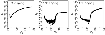
도 7은 본 발명의 실시예와 비교예에 따라 증착 직후(as-dep) 하부 게이트(bottom gate) 코-플래너(co-planar) 구조의 박막 트랜지스터의 전류-전압 특성을 나타낸 그래프이다.
도 8은 본 발명의 실시예와 비교예에 따라 증착 후 300℃에서 대기(air) 어닐링된(as-annealed) 하부 게이트(bottom gate) 코-플래너(co-planar) 구조의 박막 트랜지스터의 전류-전압 특성을 나타낸 그래프이다.
도 9는 본 발명의 실시예와 비교예에 따라 증착 후 400℃에서 대기(air) 어닐링된(as-annealed) 하부 게이트(bottom gate) 코-플래너(co-planar) 구조의 박막 트랜지스터의 전류-전압 특성을 나타낸 그래프이다.
도 10 본 발명의 실시예와 비교예에 따라 증착 후 500℃에서 대기(air) 어닐링된(as-annealed) 하부 게이트(bottom gate) 코-플래너(co-planar) 구조의 박막 트랜지스터의 전류-전압 특성을 나타낸 그래프이다.
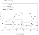
도 11은 본 발명의 실시예와 비교예에 따른 알루미늄 도핑 주석 산화물 채널층의 증착 직후(as-dep) XRD 결과이다.
도 12는 본 발명의 실시예와 비교예에 따른 알루미늄 도핑 주석 산화물 채널층의 증착 후 300℃에서 대기(air) 어닐링된(as-annealed) XRD 결과이다.
도 13은 본 발명의 실시예와 비교예에 따른 알루미늄 도핑 주석 산화물 채널층의 증착 후 400℃에서 대기(air) 어닐링된(as-annealed) XRD 결과이다.
도 14는 본 발명의 실시예와 비교예에 따른 알루미늄 도핑 주석 산화물 채널층의 증착 후 500℃에서 대기(air) 어닐링된(as-annealed) XRD 결과이다.


30: 게이트 절연막 40: 소스/드레인 전극
50: 채널층 60: 알루미늄 도핑층
Claims (11)
- 베이스 기판;
상기 베이스 기판 상에 위치하는 게이트 전극;
상기 게이트 전극 상에 위치하는 게이트 절연층;
상기 게이트 절연층 상에 위치하는 채널층;
상기 게이트 절연층 상에 위치하며 상기 채널층을 사이에 두고 상호 이격된 소스 전극과 드레인 전극;을 포함하고,
상기 채널층은 알루미늄이 도핑된 이산화 주석을 포함하며, 전하농도가 1016~1018/㎤인 것;을 특징으로 하는 박막 트랜지스터.
- 제1항에 있어서,
상기 박막 트랜지스터는 전하 이동도(field effect mobility)가 0.1~4 ㎠/Vs인 것;을 특징으로 하는 박막 트랜지스터.
- 제1항에 있어서,
상기 박막 트랜지스터는 온/오프 전류 비가 (1~10)*106 인 것;을 특징으로 하는 박막 트랜지스터.
- 제1항에 있어서,
상기 채널층의 대기(air) 어닐링 후 XRD 반치 전폭(full width half maximum)은 (200)면 피크를 기준으로 도핑되지 않은 주석 산화물(SnO2)의 대기 어닐링 후 XRD 반치 전폭보다 1.6배 내지 2.13배 큰 것;을 특징으로 하는 박막 트랜지스터.
- 기판 상에 게이트 전극을 형성하는 공정;
상기 게이트 전극 상에 게이트 절연층을 형성하는 공정;
상기 게이트 절연층 상에 채널층을 형성하는 공정;
상기 게이트 절연층 상에 위치하며 상기 채널층을 사이에 두고 상호 이격된 소스 전극과 드레인 전극을 형성하는 공정;
어닐링 공정;을 포함하고,
상기 채널층을 형성하는 공정은 주석 산화물(SnOx) 사이클/아르곤(Ar) 퍼징/알루미늄 산화물(Al2O3) 사이클/아르곤 퍼징 단계를 포함하며, 상기 알루미늄 산화물(Al2O3) 사이클은 복수 회 수행되는 주석 산화물(SnOx) 사이클의 중간 단계에 수행되는 것;을 특징으로 하는 박막 트랜지스터의 제조 방법.
- 제5항에 있어서,
상기 주석 산화물(SnOx) 사이클은 원자층 증착법(ALD)을 이용하며, 각 단계는 주석 화학종을 공급하여 기판 위에 주석 화학종을 흡착시키는 단계/아르곤 퍼징 단계/산소 원을 공급하여 주석 화학종이 흡착된 기판 위에 산소 화학종을 흡착시켜 산화 반응을 일으키는 단계/아르곤 퍼징 단계를 포함하는 것;을 특징으로 하는 박막 트랜지스터의 제조 방법.
- 제6항에 있어서,
상기 주석 화학종은 4가 주석 전구체를 포함하고, 상기 산소 원은 오존 또는 산소인 것;을 특징으로 하는 박막 트랜지스터의 제조 방법.
- 제5항에 있어서,
상기 어닐링 공정은 대기(air)에서 300~500℃ 온도범위에서 수행되는 것; 을 특징으로 하는 박막 트랜지스터의 제조 방법.
- 제8항에 있어서,
상기 어닐링 공정 후 상기 채널층의 전하농도는 1016~1018/㎤인 것;을 특징으로 하는 박막 트랜지스터의 제조 방법.
- 제8항에 있어서,
상기 어닐링 공정 후 상기 박막 트랜지스터의 전하 이동도(field effect mobility)는 0.1~4 ㎠/Vs이고, 온/오프 전류 비는 (1~10)*106 인 것;을 특징으로 하는 박막 트랜지스터의 제조 방법.
- 제8항에 있어서,
상기 어닐링 공정 후 상기 채널층의 XRD 반치 전폭(full width half maximum)은 (200)면 피크를 기준으로 도핑되지 않은 주석 산화물(SnO2)의 XRD 반치 전폭보다 1.6배 내지 2.13배 큰 것;
을 특징으로 하는 박막 트랜지스터의 제조 방법.
Priority Applications (2)
| Application Number | Priority Date | Filing Date | Title |
|---|---|---|---|
| KR1020180141672A KR102660923B1 (ko) | 2018-11-16 | 2018-11-16 | 도핑된 주석 산화물 박막 트랜지스터 및 그 제조 방법 |
| PCT/KR2019/011723 WO2020101164A1 (ko) | 2018-11-16 | 2019-09-10 | 도핑된 주석 산화물 박막 트랜지스터 및 그 제조 방법 |
Applications Claiming Priority (1)
| Application Number | Priority Date | Filing Date | Title |
|---|---|---|---|
| KR1020180141672A KR102660923B1 (ko) | 2018-11-16 | 2018-11-16 | 도핑된 주석 산화물 박막 트랜지스터 및 그 제조 방법 |
Publications (2)
| Publication Number | Publication Date |
|---|---|
| KR20200057372A true KR20200057372A (ko) | 2020-05-26 |
| KR102660923B1 KR102660923B1 (ko) | 2024-04-24 |
Family
ID=70732189
Family Applications (1)
| Application Number | Title | Priority Date | Filing Date |
|---|---|---|---|
| KR1020180141672A Active KR102660923B1 (ko) | 2018-11-16 | 2018-11-16 | 도핑된 주석 산화물 박막 트랜지스터 및 그 제조 방법 |
Country Status (2)
| Country | Link |
|---|---|
| KR (1) | KR102660923B1 (ko) |
| WO (1) | WO2020101164A1 (ko) |
Citations (1)
| Publication number | Priority date | Publication date | Assignee | Title |
|---|---|---|---|---|
| KR20090110193A (ko) * | 2008-04-16 | 2009-10-21 | 한국전자통신연구원 | 산화물 반도체 박막용 조성물, 이를 채용한 전계 효과트랜지스터 및 이의 제조방법 |
Family Cites Families (2)
| Publication number | Priority date | Publication date | Assignee | Title |
|---|---|---|---|---|
| KR101608887B1 (ko) * | 2009-04-17 | 2016-04-05 | 삼성전자주식회사 | 인버터와 그 제조방법 및 인버터를 포함하는 논리회로 |
| JP2018022879A (ja) * | 2016-07-20 | 2018-02-08 | 株式会社リコー | 電界効果型トランジスタ、及びその製造方法、並びに表示素子、画像表示装置、及びシステム |
-
2018
- 2018-11-16 KR KR1020180141672A patent/KR102660923B1/ko active Active
-
2019
- 2019-09-10 WO PCT/KR2019/011723 patent/WO2020101164A1/ko not_active Ceased
Patent Citations (1)
| Publication number | Priority date | Publication date | Assignee | Title |
|---|---|---|---|---|
| KR20090110193A (ko) * | 2008-04-16 | 2009-10-21 | 한국전자통신연구원 | 산화물 반도체 박막용 조성물, 이를 채용한 전계 효과트랜지스터 및 이의 제조방법 |
Non-Patent Citations (3)
| Title |
|---|
| Annealing Effect on Al doped SnO2 Nano structure Thin Films Prepared by Spray Pyrolysis Technique, Journal of Nanoscience and Technology(JACS), Volume 4, Issue 1, 페이지 317-319(2018.03.31.) 1부.* * |
| Performance Enhancements in p-Type Al-Doped Tin-Oxide Thin Film Transistors by Using Fluorine Plasma Treatment, IEEE Electron Device Letters, Volume 38, Issue 2(2016.12.29.) 1부.* * |
| Structural, electrical, and optical properties of atomic layer deposition Aldoped ZnO films, Journal of Applied Physics(AIP), Volume 108, Issue 4(2010.08.17.) 1부.* * |
Also Published As
| Publication number | Publication date |
|---|---|
| WO2020101164A1 (ko) | 2020-05-22 |
| KR102660923B1 (ko) | 2024-04-24 |
Similar Documents
| Publication | Publication Date | Title |
|---|---|---|
| KR101638978B1 (ko) | 박막 트랜지스터 및 그 제조방법 | |
| US8026506B2 (en) | Thin-film transistor with channel layer formed by metal oxide film including indium, and method of manufacturing the same | |
| KR100785038B1 (ko) | 비정질 ZnO계 TFT | |
| KR101980196B1 (ko) | 트랜지스터와 그 제조방법 및 트랜지스터를 포함하는 전자소자 | |
| JP5538797B2 (ja) | 電界効果型トランジスタ及び表示装置 | |
| JP6338361B2 (ja) | 半導体物質とそれを含む薄膜トランジスタ及び該薄膜トランジスタを含む電子素子 | |
| JP5704790B2 (ja) | 薄膜トランジスタ、および、表示装置 | |
| US9087907B2 (en) | Thin film transistor and method of manufacturing the same | |
| KR100918404B1 (ko) | 박막 트랜지스터 및 이를 이용한 평판 표시 장치 | |
| KR100857455B1 (ko) | 산화물 반도체막상에 보호막을 형성하여 패터닝하는 박막트랜지스터의 제조방법 | |
| US20120037897A1 (en) | Thin film transistor and method for manufacturing thin film transistor | |
| TWI405335B (zh) | 半導體結構及其製造方法 | |
| KR20110028385A (ko) | 고 성능 금속 산화물 및 금속 산질화물 박막 트랜지스터들을 제조하기 위한 게이트 유전체의 처리 | |
| TW200937534A (en) | Method for manufacturing field-effect transistor | |
| KR101372734B1 (ko) | 액상공정을 이용한 박막 트랜지스터 및 그 제조방법 | |
| KR101975929B1 (ko) | 질산화물 채널층을 구비한 트랜지스터 및 그 제조방법 | |
| JP2010123913A (ja) | 薄膜トランジスタ及びその製造方法 | |
| KR100990217B1 (ko) | 산화물 반도체 박막용 조성물, 이를 채용한 전계 효과트랜지스터 및 이의 제조방법 | |
| CN104124281B (zh) | 双极性薄膜晶体管及其制备方法 | |
| KR102000829B1 (ko) | 고유전체 절연 박막을 포함하는 박막 트랜지스터 및 이의 제조 방법 | |
| JP2011258804A (ja) | 電界効果型トランジスタ及びその製造方法 | |
| KR101417932B1 (ko) | 이중층 구조의 반도체 채널을 구비하는 박막트랜지스터 및 이의 제조방법 | |
| CN101997037B (zh) | 半导体结构及其制造方法 | |
| KR101876011B1 (ko) | 산화물 박막 트랜지스터 및 그 제조방법 | |
| KR102509588B1 (ko) | 이종접합 igzo 채널층을 구비하는 박막트랜지스터 |
Legal Events
| Date | Code | Title | Description |
|---|---|---|---|
| PA0109 | Patent application |
St.27 status event code: A-0-1-A10-A12-nap-PA0109 |
|
| R18-X000 | Changes to party contact information recorded |
St.27 status event code: A-3-3-R10-R18-oth-X000 |
|
| R18-X000 | Changes to party contact information recorded |
St.27 status event code: A-3-3-R10-R18-oth-X000 |
|
| PG1501 | Laying open of application |
St.27 status event code: A-1-1-Q10-Q12-nap-PG1501 |
|
| PA0201 | Request for examination |
St.27 status event code: A-1-2-D10-D11-exm-PA0201 |
|
| E902 | Notification of reason for refusal | ||
| PE0902 | Notice of grounds for rejection |
St.27 status event code: A-1-2-D10-D21-exm-PE0902 |
|
| T11-X000 | Administrative time limit extension requested |
St.27 status event code: U-3-3-T10-T11-oth-X000 |
|
| T11-X000 | Administrative time limit extension requested |
St.27 status event code: U-3-3-T10-T11-oth-X000 |
|
| AMND | Amendment | ||
| P11-X000 | Amendment of application requested |
St.27 status event code: A-2-2-P10-P11-nap-X000 |
|
| P13-X000 | Application amended |
St.27 status event code: A-2-2-P10-P13-nap-X000 |
|
| E601 | Decision to refuse application | ||
| PE0601 | Decision on rejection of patent |
St.27 status event code: N-2-6-B10-B15-exm-PE0601 |
|
| X091 | Application refused [patent] | ||
| AMND | Amendment | ||
| E13-X000 | Pre-grant limitation requested |
St.27 status event code: A-2-3-E10-E13-lim-X000 |
|
| P11-X000 | Amendment of application requested |
St.27 status event code: A-2-2-P10-P11-nap-X000 |
|
| P13-X000 | Application amended |
St.27 status event code: A-2-2-P10-P13-nap-X000 |
|
| PX0901 | Re-examination |
St.27 status event code: A-2-3-E10-E12-rex-PX0901 |
|
| PX0701 | Decision of registration after re-examination |
St.27 status event code: A-3-4-F10-F13-rex-PX0701 |
|
| X701 | Decision to grant (after re-examination) | ||
| GRNT | Written decision to grant | ||
| PR0701 | Registration of establishment |
St.27 status event code: A-2-4-F10-F11-exm-PR0701 |
|
| PR1002 | Payment of registration fee |
St.27 status event code: A-2-2-U10-U11-oth-PR1002 Fee payment year number: 1 |
|
| PG1601 | Publication of registration |
St.27 status event code: A-4-4-Q10-Q13-nap-PG1601 |
|
| P22-X000 | Classification modified |
St.27 status event code: A-4-4-P10-P22-nap-X000 |
|
| P22-X000 | Classification modified |
St.27 status event code: A-4-4-P10-P22-nap-X000 |