KR20200057776A - 리소그래피 클러스터, 리소그래피 장치, 및 디바이스 제조 방법 - Google Patents
리소그래피 클러스터, 리소그래피 장치, 및 디바이스 제조 방법 Download PDFInfo
- Publication number
- KR20200057776A KR20200057776A KR1020207012709A KR20207012709A KR20200057776A KR 20200057776 A KR20200057776 A KR 20200057776A KR 1020207012709 A KR1020207012709 A KR 1020207012709A KR 20207012709 A KR20207012709 A KR 20207012709A KR 20200057776 A KR20200057776 A KR 20200057776A
- Authority
- KR
- South Korea
- Prior art keywords
- alignment
- lot
- wafer
- mark
- lithographic apparatus
- Prior art date
- Legal status (The legal status is an assumption and is not a legal conclusion. Google has not performed a legal analysis and makes no representation as to the accuracy of the status listed.)
- Granted
Links
Images





Classifications
-
- G—PHYSICS
- G03—PHOTOGRAPHY; CINEMATOGRAPHY; ANALOGOUS TECHNIQUES USING WAVES OTHER THAN OPTICAL WAVES; ELECTROGRAPHY; HOLOGRAPHY
- G03F—PHOTOMECHANICAL PRODUCTION OF TEXTURED OR PATTERNED SURFACES, e.g. FOR PRINTING, FOR PROCESSING OF SEMICONDUCTOR DEVICES; MATERIALS THEREFOR; ORIGINALS THEREFOR; APPARATUS SPECIALLY ADAPTED THEREFOR
- G03F9/00—Registration or positioning of originals, masks, frames, photographic sheets or textured or patterned surfaces, e.g. automatically
- G03F9/70—Registration or positioning of originals, masks, frames, photographic sheets or textured or patterned surfaces, e.g. automatically for microlithography
- G03F9/7003—Alignment type or strategy, e.g. leveling, global alignment
- G03F9/7019—Calibration
-
- G—PHYSICS
- G03—PHOTOGRAPHY; CINEMATOGRAPHY; ANALOGOUS TECHNIQUES USING WAVES OTHER THAN OPTICAL WAVES; ELECTROGRAPHY; HOLOGRAPHY
- G03F—PHOTOMECHANICAL PRODUCTION OF TEXTURED OR PATTERNED SURFACES, e.g. FOR PRINTING, FOR PROCESSING OF SEMICONDUCTOR DEVICES; MATERIALS THEREFOR; ORIGINALS THEREFOR; APPARATUS SPECIALLY ADAPTED THEREFOR
- G03F7/00—Photomechanical, e.g. photolithographic, production of textured or patterned surfaces, e.g. printing surfaces; Materials therefor, e.g. comprising photoresists; Apparatus specially adapted therefor
- G03F7/70—Microphotolithographic exposure; Apparatus therefor
- G03F7/70483—Information management; Active and passive control; Testing; Wafer monitoring, e.g. pattern monitoring
- G03F7/70605—Workpiece metrology
- G03F7/70616—Monitoring the printed patterns
- G03F7/70633—Overlay, i.e. relative alignment between patterns printed by separate exposures in different layers, or in the same layer in multiple exposures or stitching
-
- G—PHYSICS
- G03—PHOTOGRAPHY; CINEMATOGRAPHY; ANALOGOUS TECHNIQUES USING WAVES OTHER THAN OPTICAL WAVES; ELECTROGRAPHY; HOLOGRAPHY
- G03F—PHOTOMECHANICAL PRODUCTION OF TEXTURED OR PATTERNED SURFACES, e.g. FOR PRINTING, FOR PROCESSING OF SEMICONDUCTOR DEVICES; MATERIALS THEREFOR; ORIGINALS THEREFOR; APPARATUS SPECIALLY ADAPTED THEREFOR
- G03F7/00—Photomechanical, e.g. photolithographic, production of textured or patterned surfaces, e.g. printing surfaces; Materials therefor, e.g. comprising photoresists; Apparatus specially adapted therefor
- G03F7/70—Microphotolithographic exposure; Apparatus therefor
- G03F7/70483—Information management; Active and passive control; Testing; Wafer monitoring, e.g. pattern monitoring
- G03F7/70605—Workpiece metrology
- G03F7/706843—Metrology apparatus
- G03F7/706845—Calibration, e.g. tool-to-tool calibration, beam alignment, spot position or focus
-
- G—PHYSICS
- G03—PHOTOGRAPHY; CINEMATOGRAPHY; ANALOGOUS TECHNIQUES USING WAVES OTHER THAN OPTICAL WAVES; ELECTROGRAPHY; HOLOGRAPHY
- G03F—PHOTOMECHANICAL PRODUCTION OF TEXTURED OR PATTERNED SURFACES, e.g. FOR PRINTING, FOR PROCESSING OF SEMICONDUCTOR DEVICES; MATERIALS THEREFOR; ORIGINALS THEREFOR; APPARATUS SPECIALLY ADAPTED THEREFOR
- G03F9/00—Registration or positioning of originals, masks, frames, photographic sheets or textured or patterned surfaces, e.g. automatically
- G03F9/70—Registration or positioning of originals, masks, frames, photographic sheets or textured or patterned surfaces, e.g. automatically for microlithography
- G03F9/7073—Alignment marks and their environment
-
- G—PHYSICS
- G03—PHOTOGRAPHY; CINEMATOGRAPHY; ANALOGOUS TECHNIQUES USING WAVES OTHER THAN OPTICAL WAVES; ELECTROGRAPHY; HOLOGRAPHY
- G03F—PHOTOMECHANICAL PRODUCTION OF TEXTURED OR PATTERNED SURFACES, e.g. FOR PRINTING, FOR PROCESSING OF SEMICONDUCTOR DEVICES; MATERIALS THEREFOR; ORIGINALS THEREFOR; APPARATUS SPECIALLY ADAPTED THEREFOR
- G03F9/00—Registration or positioning of originals, masks, frames, photographic sheets or textured or patterned surfaces, e.g. automatically
- G03F9/70—Registration or positioning of originals, masks, frames, photographic sheets or textured or patterned surfaces, e.g. automatically for microlithography
- G03F9/7092—Signal processing
-
- H01L22/20—
-
- H—ELECTRICITY
- H10—SEMICONDUCTOR DEVICES; ELECTRIC SOLID-STATE DEVICES NOT OTHERWISE PROVIDED FOR
- H10P—GENERIC PROCESSES OR APPARATUS FOR THE MANUFACTURE OR TREATMENT OF DEVICES COVERED BY CLASS H10
- H10P74/00—Testing or measuring during manufacture or treatment of wafers, substrates or devices
- H10P74/23—Testing or measuring during manufacture or treatment of wafers, substrates or devices characterised by multiple measurements, corrections, marking or sorting processes
-
- H—ELECTRICITY
- H10—SEMICONDUCTOR DEVICES; ELECTRIC SOLID-STATE DEVICES NOT OTHERWISE PROVIDED FOR
- H10P—GENERIC PROCESSES OR APPARATUS FOR THE MANUFACTURE OR TREATMENT OF DEVICES COVERED BY CLASS H10
- H10P74/00—Testing or measuring during manufacture or treatment of wafers, substrates or devices
- H10P74/20—Testing or measuring during manufacture or treatment of wafers, substrates or devices characterised by the properties tested or measured, e.g. structural or electrical properties
- H10P74/203—Structural properties, e.g. testing or measuring thicknesses, line widths, warpage, bond strengths or physical defects
Landscapes
- Physics & Mathematics (AREA)
- General Physics & Mathematics (AREA)
- Engineering & Computer Science (AREA)
- Signal Processing (AREA)
- Exposure And Positioning Against Photoresist Photosensitive Materials (AREA)
Abstract
Description
도 1은 어떤 실시 형태에 따른 리소그래피 장치를 나타낸다.
도 2는 어떤 실시 형태에 따른, 리소그래피 장치를 갖는 리소그래피 클러스터를 나타낸다.
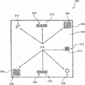
도 3은 어떤 실시 형태에 따른 교정 웨이퍼의 개략도를 나타낸다.
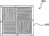
도 4a - 4c는 어떤 실시 형태에 따른 서로 다른 정렬 마크 유형들의 평면도를 나타낸다.
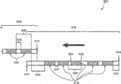
도 5는 어떤 실시 형태에 따른, 스트리밍 모드로 있는 리소그래피 클러스터의 웨이퍼 처리 흐름의 개략도를 나타낸다.
도 6은 어떤 실시 형태에 따른, 오버레이 드리프트 또는 점프를 완화하기 위한 흐름도를 나타낸다.
본 발명의 특징 및 이점은 도면과 함께 아래에 주어진 상세한 설명으로부터 더 명백하게 될 것이고, 도면에서 유사한 참조 번호는 전체에 걸쳐 대응하는 요소를 나타낸다. 도면에서, 유사한 참조 번호는 일반적으로 동일하거나, 기능적으로 유사하고 그리고/또는 구조적으로 유사한 요소를 나타낸다. 추가로, 일반적으로, 참조 번호의 가장 좌측의 자리는 그 참조 번호가 가장 먼저 나타나는 도를 나타낸다. 다른 지시가 없으면, 본 개시 전체에 결쳐 제공되어 있는 도면은 척도에 따른 도면으로 해석되어서는 안 된다.
Claims (15)
- 리소그래피 클러스터로서,
복수의 제 1 웨이퍼를 포함하는 제 1 로트(lot) 및 복수의 제 2 웨이퍼를 포함하는 제 2 로트를 처리하도록 구성된 트랙 유닛, 및
상기 트랙 유닛에 작동적으로 연결되는 리소그래피 장치를 포함하고,
상기 리소그래피 장치는,
교정 웨이퍼의 적어도 하나의 정렬 마크 타입(mark type)의 정렬을 측정하도록 구성된 정렬 센서, 및
적어도 하나의 제어기를 포함하고,
상기 제어기는,
상기 적어도 하나의 정렬 마크 타입의 측정된 정렬에 근거하여 리소그래피 장치를 교정하기 위한 보정치 세트를 결정하고,
상기 제 1 로트를 처리하기 위해 제 1 가중 보정치를 상기 보정치 세트에 가하며, 또한
상기 제 2 로트를 처리하기 위해 제 2 가중 보정치를 상기 보정치 세트에 가하도록 구성되어 있고,
상기 제 1 및 제 2 로트의 처리 동안의 오버레이 드리프트(overlay drift) 또는 점프가 완화되도록 상기 제 2 가중 보정치는 제 1 가중 보정치 이상인, 리소그래피 클러스터. - 제 1 항에 있어서,
상기 트랙 유닛은 상기 교정 웨이퍼를 스트리밍시키고 처리하도록 더 구성되어 있는, 리소그래피 클러스터. - 제 1 항에 있어서,
상기 교정 웨이퍼는 엣칭된 그리고 코팅되지 않은 웨이퍼인, 리소그래피 클러스터. - 제 1 항에 있어서,
상기 교정 웨이퍼는 코팅되어 있는, 리소그래피 클러스터. - 제 1 항에 있어서,
상기 트랙 유닛 및 리소그래피 장치는, 상기 제 2 로트를 처리하기 위한 시작 시간이 제 1 로트를 처리하기 위한 마무리 시간 전에 일어나도록 제 1 로트와 제 2 로트를 스트리밍시키도록 구성되어 있는, 리소그래피 클러스터. - 제 1 항에 있어서,
상기 교정 웨이퍼가 제 1 로트 및 제 2 로트에 앞서 스트리밍되고 있는 동안에 상기 정렬 센서는 상기 교정 웨이퍼의 상기 적어도 하나의 정렬 마크 타입의 정렬을 측정하는, 리소그래피 클러스터. - 제 1 항에 있어서,
상기 교정 웨이퍼의 적어도 하나의 정렬 마크 타입은 2-방향 미세 웨이퍼 정렬(BF) 마크를 포함하는, 리소그래피 클러스터. - 제 1 항에 있어서,
상기 교정 웨이퍼의 적어도 하나의 정렬 마크 타입은 대칭형 미세 웨이퍼 정렬(SF) 마크를 포함하는, 리소그래피 클러스터. - 제 1 항에 있어서,
상기 제 1 가중 보정치를 가하는 것 및 제 2 가중 보정치를 가하는 것 각각은, 애플리케이션 특정적 보정(ASC), 동적 애플리케이션 특정적 보정(ASC2), 애플리케이션 공정 보정(APC), 내부 APC 루프 또는 이것들의 특정 조합의 실행을 포함하는, 리소그래피 클러스터. - 리소그래피 클러스터에서 오버레이 드리프트 또는 점프를 완화하기 위한 방법으로서,
정렬 센서를 사용하여, 교정 웨이퍼의 적어도 하나의 정렬 마크 타입의 정렬을 측정하는 단계,
적어도 하나의 제어기를 사용하여, 상기 적어도 하나의 정렬 마크 타입의 측정된 정렬에 근거하여 보정치 세트를 결정하는 단계; 및
리소그래피 장치를 사용하여, 제 1 가중 보정치를 상기 보정치 세트에 가하여 복수의 제 1 웨이퍼를 포함하는 제 1 로트를 처리하고, 또한 제 2 가중 보정치를 상기 보정치 세트에 가하여 복수의 제 2 웨이퍼를 포함하는 제 2 로트를 처리하는 단계를 포함하는, 오버레이 드리프트 또는 점프를 완화하기 위한 방법. - 제 10 항에 있어서,
처리는, 상기 제 2 로트의 시작 시간이 제 1 로트의 마무리 시간 전에 일어나도록 제 1 로트와 제 2 로트를 스트리밍시키는 것을 포함하는, 방법. - 제 10 항에 있어서,
처리는 실시간으로 일어나는, 방법. - 제 10 항에 있어서,
상기 교정 웨이퍼를 상기 제 1 및 제 2 로트에 앞서 스트리밍시키는 단계를 더 포함하고, 그래서, 교정 웨이퍼의 측정된 정렬에 근거하는 보정치 세트가 결정된 후에, 상기 제 1 로트를 처리하는 시작 시간이 일어나는, 방법. - 제 10 항에 있어서,
상기 교정 웨이퍼의 적어도 하나의 정렬 마크 타입은 2-방향 미세 웨이퍼 정렬(BF) 마크, 대칭형 미세 웨이퍼 정렬(SF) 마크, 맞춤형 마크 또는 이것들의 특정 조합을 포함하는, 방법. - 제 10 항에 있어서,
상기 제 2 가중 보정치는 제 1 가중 보정치 이상인, 방법.
Applications Claiming Priority (3)
| Application Number | Priority Date | Filing Date | Title |
|---|---|---|---|
| US201762580095P | 2017-11-01 | 2017-11-01 | |
| US62/580,095 | 2017-11-01 | ||
| PCT/EP2018/079364 WO2019086334A1 (en) | 2017-11-01 | 2018-10-26 | Lithographic cluster, lithographic apparatus, and device manufacturing method |
Publications (2)
| Publication Number | Publication Date |
|---|---|
| KR20200057776A true KR20200057776A (ko) | 2020-05-26 |
| KR102394346B1 KR102394346B1 (ko) | 2022-05-03 |
Family
ID=64109822
Family Applications (1)
| Application Number | Title | Priority Date | Filing Date |
|---|---|---|---|
| KR1020207012709A Active KR102394346B1 (ko) | 2017-11-01 | 2018-10-26 | 리소그래피 클러스터, 리소그래피 장치, 및 디바이스 제조 방법 |
Country Status (6)
| Country | Link |
|---|---|
| US (1) | US10895813B2 (ko) |
| KR (1) | KR102394346B1 (ko) |
| CN (1) | CN111316170A (ko) |
| NL (1) | NL2021881A (ko) |
| TW (1) | TWI696884B (ko) |
| WO (1) | WO2019086334A1 (ko) |
Cited By (2)
| Publication number | Priority date | Publication date | Assignee | Title |
|---|---|---|---|---|
| KR20230020998A (ko) * | 2020-06-08 | 2023-02-13 | 케이엘에이 코포레이션 | 비지도 학습 및 적응형 데이터베이스 생성 방법을 이용한 표본 내 변형 및 표본 간 변형을 가진 표본들에 대한 이미지 정렬 셋업 |
| KR20240083498A (ko) * | 2022-12-05 | 2024-06-12 | 이재준 | 설비 진단을 위한 스테이지 마크를 이용한 설비 진단 시스템 및 이를 이용한 설비 진단 방법 |
Families Citing this family (3)
| Publication number | Priority date | Publication date | Assignee | Title |
|---|---|---|---|---|
| US10831110B2 (en) * | 2018-05-29 | 2020-11-10 | Taiwan Semiconductor Manufacturing Company Ltd. | Lithographic overlay correction and lithographic process |
| JP7356585B2 (ja) * | 2019-10-08 | 2023-10-04 | アプライド マテリアルズ インコーポレイテッド | マスクレスリソグラフィシステム用ユニバーサル計測ファイル、プロトコル、及びプロセス |
| CN112838017A (zh) * | 2019-11-22 | 2021-05-25 | 长鑫存储技术有限公司 | 光刻图形检测方法及系统 |
Citations (4)
| Publication number | Priority date | Publication date | Assignee | Title |
|---|---|---|---|---|
| US20020012861A1 (en) * | 2000-07-31 | 2002-01-31 | Gerhard Luhn | Control system for photolithographic processes |
| EP1843210A2 (en) * | 2006-04-04 | 2007-10-10 | ASML Netherlands BV | Method of aligning and exposing a substrate |
| US20100030360A1 (en) * | 2008-08-01 | 2010-02-04 | Boris Habets | Alignment Calculation |
| US20140212817A1 (en) * | 2013-01-25 | 2014-07-31 | Boris Habets | Method and apparatus for fabricating wafer by calculating process correction parameters |
Family Cites Families (11)
| Publication number | Priority date | Publication date | Assignee | Title |
|---|---|---|---|---|
| JP2839081B2 (ja) * | 1996-03-06 | 1998-12-16 | 日本電気株式会社 | 半導体装置の製造方法 |
| JP3570728B2 (ja) | 1997-03-07 | 2004-09-29 | アーエスエム リソグラフィ ベスローテン フェンノートシャップ | 離軸整列ユニットを持つリトグラフ投射装置 |
| KR100431329B1 (ko) * | 2001-10-11 | 2004-05-12 | 삼성전자주식회사 | 반도체 웨이퍼 오버레이 보정방법 |
| DE60319462T2 (de) | 2002-06-11 | 2009-03-12 | Asml Netherlands B.V. | Lithographischer Apparat und Verfahren zur Herstellung eines Artikels |
| WO2008117444A1 (ja) * | 2007-03-27 | 2008-10-02 | Fujitsu Limited | リソグラフィ処理の露光位置アライメント方法 |
| CN102460310B (zh) | 2009-06-17 | 2014-07-02 | Asml荷兰有限公司 | 重叠测量的方法、光刻设备、检查设备、处理设备和光刻处理单元 |
| EP2537069B1 (en) * | 2010-02-19 | 2020-03-04 | ASML Netherlands BV | Lithographic apparatus and device manufacturing method |
| WO2016128190A1 (en) * | 2015-02-12 | 2016-08-18 | Asml Netherlands B.V. | Method and apparatus for reticle optimization |
| US9672320B2 (en) | 2015-06-30 | 2017-06-06 | Taiwan Semiconductor Manufacturing Company, Ltd. | Method for integrated circuit manufacturing |
| KR102387289B1 (ko) * | 2015-07-20 | 2022-04-14 | 에이에스엠엘 네델란즈 비.브이. | 리소그래피 장치를 제어하는 방법, 리소그래피 장치 및 디바이스 제조 방법 |
| CN108431695B (zh) | 2015-12-24 | 2020-07-21 | Asml荷兰有限公司 | 控制图案形成过程的方法、器件制造方法、用于光刻设备的控制系统以及光刻设备 |
-
2018
- 2018-10-26 WO PCT/EP2018/079364 patent/WO2019086334A1/en not_active Ceased
- 2018-10-26 TW TW107137873A patent/TWI696884B/zh active
- 2018-10-26 NL NL2021881A patent/NL2021881A/en unknown
- 2018-10-26 CN CN201880071423.9A patent/CN111316170A/zh active Pending
- 2018-10-26 US US16/760,137 patent/US10895813B2/en active Active
- 2018-10-26 KR KR1020207012709A patent/KR102394346B1/ko active Active
Patent Citations (4)
| Publication number | Priority date | Publication date | Assignee | Title |
|---|---|---|---|---|
| US20020012861A1 (en) * | 2000-07-31 | 2002-01-31 | Gerhard Luhn | Control system for photolithographic processes |
| EP1843210A2 (en) * | 2006-04-04 | 2007-10-10 | ASML Netherlands BV | Method of aligning and exposing a substrate |
| US20100030360A1 (en) * | 2008-08-01 | 2010-02-04 | Boris Habets | Alignment Calculation |
| US20140212817A1 (en) * | 2013-01-25 | 2014-07-31 | Boris Habets | Method and apparatus for fabricating wafer by calculating process correction parameters |
Cited By (2)
| Publication number | Priority date | Publication date | Assignee | Title |
|---|---|---|---|---|
| KR20230020998A (ko) * | 2020-06-08 | 2023-02-13 | 케이엘에이 코포레이션 | 비지도 학습 및 적응형 데이터베이스 생성 방법을 이용한 표본 내 변형 및 표본 간 변형을 가진 표본들에 대한 이미지 정렬 셋업 |
| KR20240083498A (ko) * | 2022-12-05 | 2024-06-12 | 이재준 | 설비 진단을 위한 스테이지 마크를 이용한 설비 진단 시스템 및 이를 이용한 설비 진단 방법 |
Also Published As
| Publication number | Publication date |
|---|---|
| US10895813B2 (en) | 2021-01-19 |
| KR102394346B1 (ko) | 2022-05-03 |
| TW201923445A (zh) | 2019-06-16 |
| US20200326640A1 (en) | 2020-10-15 |
| WO2019086334A1 (en) | 2019-05-09 |
| TWI696884B (zh) | 2020-06-21 |
| CN111316170A (zh) | 2020-06-19 |
| NL2021881A (en) | 2019-05-06 |
Similar Documents
| Publication | Publication Date | Title |
|---|---|---|
| US12050406B2 (en) | Method for controlling a lithographic apparatus and associated apparatuses | |
| US11493851B2 (en) | Lithographic method and lithographic apparatus | |
| US10025193B2 (en) | Lithographic apparatus, device manufacturing method and associated data processing apparatus and computer program product | |
| CN102754035B (zh) | 光刻设备和器件制造方法 | |
| KR102394346B1 (ko) | 리소그래피 클러스터, 리소그래피 장치, 및 디바이스 제조 방법 | |
| US10095131B2 (en) | Alignment modeling and a lithographic apparatus and exposure method using the same | |
| TWI865583B (zh) | 判定用於微影設備之控制設定之方法及相關電腦程式產品 | |
| CN112352201A (zh) | 用于控制制造设备和相关联设备的方法 | |
| US8793099B2 (en) | Calibration of lithographic apparatus | |
| EP3848757A1 (en) | Method for controlling a lithographic apparatus | |
| TW202526524A (zh) | 微影方法及相關設備 | |
| NL2024657A (en) | Method for controlling a lithographic apparatus |
Legal Events
| Date | Code | Title | Description |
|---|---|---|---|
| PA0105 | International application |
St.27 status event code: A-0-1-A10-A15-nap-PA0105 |
|
| PA0201 | Request for examination |
St.27 status event code: A-1-2-D10-D11-exm-PA0201 |
|
| PG1501 | Laying open of application |
St.27 status event code: A-1-1-Q10-Q12-nap-PG1501 |
|
| E902 | Notification of reason for refusal | ||
| PE0902 | Notice of grounds for rejection |
St.27 status event code: A-1-2-D10-D21-exm-PE0902 |
|
| P11-X000 | Amendment of application requested |
St.27 status event code: A-2-2-P10-P11-nap-X000 |
|
| P13-X000 | Application amended |
St.27 status event code: A-2-2-P10-P13-nap-X000 |
|
| E701 | Decision to grant or registration of patent right | ||
| PE0701 | Decision of registration |
St.27 status event code: A-1-2-D10-D22-exm-PE0701 |
|
| GRNT | Written decision to grant | ||
| PR0701 | Registration of establishment |
St.27 status event code: A-2-4-F10-F11-exm-PR0701 |
|
| PR1002 | Payment of registration fee |
St.27 status event code: A-2-2-U10-U12-oth-PR1002 Fee payment year number: 1 |
|
| PG1601 | Publication of registration |
St.27 status event code: A-4-4-Q10-Q13-nap-PG1601 |
|
| P22-X000 | Classification modified |
St.27 status event code: A-4-4-P10-P22-nap-X000 |
|
| P22-X000 | Classification modified |
St.27 status event code: A-4-4-P10-P22-nap-X000 |