KR20200058575A - 다이-다이 검사를 위한 적응형 케어 영역들 - Google Patents
다이-다이 검사를 위한 적응형 케어 영역들 Download PDFInfo
- Publication number
- KR20200058575A KR20200058575A KR1020207014020A KR20207014020A KR20200058575A KR 20200058575 A KR20200058575 A KR 20200058575A KR 1020207014020 A KR1020207014020 A KR 1020207014020A KR 20207014020 A KR20207014020 A KR 20207014020A KR 20200058575 A KR20200058575 A KR 20200058575A
- Authority
- KR
- South Korea
- Prior art keywords
- care area
- die image
- adaptive care
- die
- adaptive
- Prior art date
- Legal status (The legal status is an assumption and is not a legal conclusion. Google has not performed a legal analysis and makes no representation as to the accuracy of the status listed.)
- Granted
Links
Images






Classifications
-
- H01L22/12—
-
- H—ELECTRICITY
- H10—SEMICONDUCTOR DEVICES; ELECTRIC SOLID-STATE DEVICES NOT OTHERWISE PROVIDED FOR
- H10P—GENERIC PROCESSES OR APPARATUS FOR THE MANUFACTURE OR TREATMENT OF DEVICES COVERED BY CLASS H10
- H10P74/00—Testing or measuring during manufacture or treatment of wafers, substrates or devices
- H10P74/20—Testing or measuring during manufacture or treatment of wafers, substrates or devices characterised by the properties tested or measured, e.g. structural or electrical properties
- H10P74/203—Structural properties, e.g. testing or measuring thicknesses, line widths, warpage, bond strengths or physical defects
-
- G—PHYSICS
- G06—COMPUTING OR CALCULATING; COUNTING
- G06T—IMAGE DATA PROCESSING OR GENERATION, IN GENERAL
- G06T7/00—Image analysis
- G06T7/0002—Inspection of images, e.g. flaw detection
- G06T7/0004—Industrial image inspection
- G06T7/001—Industrial image inspection using an image reference approach
-
- A—HUMAN NECESSITIES
- A61—MEDICAL OR VETERINARY SCIENCE; HYGIENE
- A61K—PREPARATIONS FOR MEDICAL, DENTAL OR TOILETRY PURPOSES
- A61K31/00—Medicinal preparations containing organic active ingredients
- A61K31/70—Carbohydrates; Sugars; Derivatives thereof
- A61K31/7088—Compounds having three or more nucleosides or nucleotides
- A61K31/7115—Nucleic acids or oligonucleotides having modified bases, i.e. other than adenine, guanine, cytosine, uracil or thymine
-
- C—CHEMISTRY; METALLURGY
- C12—BIOCHEMISTRY; BEER; SPIRITS; WINE; VINEGAR; MICROBIOLOGY; ENZYMOLOGY; MUTATION OR GENETIC ENGINEERING
- C12N—MICROORGANISMS OR ENZYMES; COMPOSITIONS THEREOF; PROPAGATING, PRESERVING, OR MAINTAINING MICROORGANISMS; MUTATION OR GENETIC ENGINEERING; CULTURE MEDIA
- C12N15/00—Mutation or genetic engineering; DNA or RNA concerning genetic engineering, vectors, e.g. plasmids, or their isolation, preparation or purification; Use of hosts therefor
- C12N15/09—Recombinant DNA-technology
- C12N15/11—DNA or RNA fragments; Modified forms thereof; Non-coding nucleic acids having a biological activity
- C12N15/115—Aptamers, i.e. nucleic acids binding a target molecule specifically and with high affinity without hybridising therewith ; Nucleic acids binding to non-nucleic acids, e.g. aptamers
-
- C—CHEMISTRY; METALLURGY
- C12—BIOCHEMISTRY; BEER; SPIRITS; WINE; VINEGAR; MICROBIOLOGY; ENZYMOLOGY; MUTATION OR GENETIC ENGINEERING
- C12N—MICROORGANISMS OR ENZYMES; COMPOSITIONS THEREOF; PROPAGATING, PRESERVING, OR MAINTAINING MICROORGANISMS; MUTATION OR GENETIC ENGINEERING; CULTURE MEDIA
- C12N15/00—Mutation or genetic engineering; DNA or RNA concerning genetic engineering, vectors, e.g. plasmids, or their isolation, preparation or purification; Use of hosts therefor
- C12N15/09—Recombinant DNA-technology
- C12N15/63—Introduction of foreign genetic material using vectors; Vectors; Use of hosts therefor; Regulation of expression
-
- G—PHYSICS
- G01—MEASURING; TESTING
- G01N—INVESTIGATING OR ANALYSING MATERIALS BY DETERMINING THEIR CHEMICAL OR PHYSICAL PROPERTIES
- G01N21/00—Investigating or analysing materials by the use of optical means, i.e. using sub-millimetre waves, infrared, visible or ultraviolet light
- G01N21/84—Systems specially adapted for particular applications
- G01N21/88—Investigating the presence of flaws or contamination
- G01N21/8851—Scan or image signal processing specially adapted therefor, e.g. for scan signal adjustment, for detecting different kinds of defects, for compensating for structures, markings, edges
-
- G—PHYSICS
- G01—MEASURING; TESTING
- G01N—INVESTIGATING OR ANALYSING MATERIALS BY DETERMINING THEIR CHEMICAL OR PHYSICAL PROPERTIES
- G01N21/00—Investigating or analysing materials by the use of optical means, i.e. using sub-millimetre waves, infrared, visible or ultraviolet light
- G01N21/84—Systems specially adapted for particular applications
- G01N21/88—Investigating the presence of flaws or contamination
- G01N21/94—Investigating contamination, e.g. dust
-
- G—PHYSICS
- G06—COMPUTING OR CALCULATING; COUNTING
- G06T—IMAGE DATA PROCESSING OR GENERATION, IN GENERAL
- G06T7/00—Image analysis
- G06T7/10—Segmentation; Edge detection
- G06T7/11—Region-based segmentation
-
- H01L22/20—
-
- H01L22/30—
-
- H—ELECTRICITY
- H10—SEMICONDUCTOR DEVICES; ELECTRIC SOLID-STATE DEVICES NOT OTHERWISE PROVIDED FOR
- H10P—GENERIC PROCESSES OR APPARATUS FOR THE MANUFACTURE OR TREATMENT OF DEVICES COVERED BY CLASS H10
- H10P74/00—Testing or measuring during manufacture or treatment of wafers, substrates or devices
- H10P74/23—Testing or measuring during manufacture or treatment of wafers, substrates or devices characterised by multiple measurements, corrections, marking or sorting processes
-
- H—ELECTRICITY
- H10—SEMICONDUCTOR DEVICES; ELECTRIC SOLID-STATE DEVICES NOT OTHERWISE PROVIDED FOR
- H10P—GENERIC PROCESSES OR APPARATUS FOR THE MANUFACTURE OR TREATMENT OF DEVICES COVERED BY CLASS H10
- H10P74/00—Testing or measuring during manufacture or treatment of wafers, substrates or devices
- H10P74/27—Structural arrangements therefor
-
- C—CHEMISTRY; METALLURGY
- C12—BIOCHEMISTRY; BEER; SPIRITS; WINE; VINEGAR; MICROBIOLOGY; ENZYMOLOGY; MUTATION OR GENETIC ENGINEERING
- C12N—MICROORGANISMS OR ENZYMES; COMPOSITIONS THEREOF; PROPAGATING, PRESERVING, OR MAINTAINING MICROORGANISMS; MUTATION OR GENETIC ENGINEERING; CULTURE MEDIA
- C12N2310/00—Structure or type of the nucleic acid
- C12N2310/10—Type of nucleic acid
- C12N2310/12—Type of nucleic acid catalytic nucleic acids, e.g. ribozymes
- C12N2310/128—Type of nucleic acid catalytic nucleic acids, e.g. ribozymes processing or releasing ribozyme
-
- C—CHEMISTRY; METALLURGY
- C12—BIOCHEMISTRY; BEER; SPIRITS; WINE; VINEGAR; MICROBIOLOGY; ENZYMOLOGY; MUTATION OR GENETIC ENGINEERING
- C12N—MICROORGANISMS OR ENZYMES; COMPOSITIONS THEREOF; PROPAGATING, PRESERVING, OR MAINTAINING MICROORGANISMS; MUTATION OR GENETIC ENGINEERING; CULTURE MEDIA
- C12N2310/00—Structure or type of the nucleic acid
- C12N2310/10—Type of nucleic acid
- C12N2310/16—Aptamers
-
- C—CHEMISTRY; METALLURGY
- C12—BIOCHEMISTRY; BEER; SPIRITS; WINE; VINEGAR; MICROBIOLOGY; ENZYMOLOGY; MUTATION OR GENETIC ENGINEERING
- C12N—MICROORGANISMS OR ENZYMES; COMPOSITIONS THEREOF; PROPAGATING, PRESERVING, OR MAINTAINING MICROORGANISMS; MUTATION OR GENETIC ENGINEERING; CULTURE MEDIA
- C12N2310/00—Structure or type of the nucleic acid
- C12N2310/30—Chemical structure
- C12N2310/35—Nature of the modification
- C12N2310/351—Conjugate
- C12N2310/3519—Fusion with another nucleic acid
-
- C—CHEMISTRY; METALLURGY
- C12—BIOCHEMISTRY; BEER; SPIRITS; WINE; VINEGAR; MICROBIOLOGY; ENZYMOLOGY; MUTATION OR GENETIC ENGINEERING
- C12N—MICROORGANISMS OR ENZYMES; COMPOSITIONS THEREOF; PROPAGATING, PRESERVING, OR MAINTAINING MICROORGANISMS; MUTATION OR GENETIC ENGINEERING; CULTURE MEDIA
- C12N2310/00—Structure or type of the nucleic acid
- C12N2310/50—Physical structure
- C12N2310/51—Physical structure in polymeric form, e.g. multimers, concatemers
-
- C—CHEMISTRY; METALLURGY
- C12—BIOCHEMISTRY; BEER; SPIRITS; WINE; VINEGAR; MICROBIOLOGY; ENZYMOLOGY; MUTATION OR GENETIC ENGINEERING
- C12N—MICROORGANISMS OR ENZYMES; COMPOSITIONS THEREOF; PROPAGATING, PRESERVING, OR MAINTAINING MICROORGANISMS; MUTATION OR GENETIC ENGINEERING; CULTURE MEDIA
- C12N2310/00—Structure or type of the nucleic acid
- C12N2310/50—Physical structure
- C12N2310/53—Physical structure partially self-complementary or closed
- C12N2310/532—Closed or circular
-
- G—PHYSICS
- G01—MEASURING; TESTING
- G01N—INVESTIGATING OR ANALYSING MATERIALS BY DETERMINING THEIR CHEMICAL OR PHYSICAL PROPERTIES
- G01N21/00—Investigating or analysing materials by the use of optical means, i.e. using sub-millimetre waves, infrared, visible or ultraviolet light
- G01N21/84—Systems specially adapted for particular applications
- G01N21/88—Investigating the presence of flaws or contamination
- G01N21/95—Investigating the presence of flaws or contamination characterised by the material or shape of the object to be examined
- G01N21/956—Inspecting patterns on the surface of objects
- G01N21/95607—Inspecting patterns on the surface of objects using a comparative method
- G01N2021/95615—Inspecting patterns on the surface of objects using a comparative method with stored comparision signal
-
- G—PHYSICS
- G01—MEASURING; TESTING
- G01N—INVESTIGATING OR ANALYSING MATERIALS BY DETERMINING THEIR CHEMICAL OR PHYSICAL PROPERTIES
- G01N21/00—Investigating or analysing materials by the use of optical means, i.e. using sub-millimetre waves, infrared, visible or ultraviolet light
- G01N21/84—Systems specially adapted for particular applications
- G01N21/88—Investigating the presence of flaws or contamination
- G01N21/95—Investigating the presence of flaws or contamination characterised by the material or shape of the object to be examined
- G01N21/9501—Semiconductor wafers
-
- G—PHYSICS
- G01—MEASURING; TESTING
- G01N—INVESTIGATING OR ANALYSING MATERIALS BY DETERMINING THEIR CHEMICAL OR PHYSICAL PROPERTIES
- G01N21/00—Investigating or analysing materials by the use of optical means, i.e. using sub-millimetre waves, infrared, visible or ultraviolet light
- G01N21/84—Systems specially adapted for particular applications
- G01N21/88—Investigating the presence of flaws or contamination
- G01N21/95—Investigating the presence of flaws or contamination characterised by the material or shape of the object to be examined
- G01N21/956—Inspecting patterns on the surface of objects
- G01N21/95607—Inspecting patterns on the surface of objects using a comparative method
-
- G—PHYSICS
- G06—COMPUTING OR CALCULATING; COUNTING
- G06T—IMAGE DATA PROCESSING OR GENERATION, IN GENERAL
- G06T2207/00—Indexing scheme for image analysis or image enhancement
- G06T2207/20—Special algorithmic details
- G06T2207/20092—Interactive image processing based on input by user
- G06T2207/20104—Interactive definition of region of interest [ROI]
-
- G—PHYSICS
- G06—COMPUTING OR CALCULATING; COUNTING
- G06T—IMAGE DATA PROCESSING OR GENERATION, IN GENERAL
- G06T2207/00—Indexing scheme for image analysis or image enhancement
- G06T2207/30—Subject of image; Context of image processing
- G06T2207/30108—Industrial image inspection
- G06T2207/30148—Semiconductor; IC; Wafer
Landscapes
- Engineering & Computer Science (AREA)
- Health & Medical Sciences (AREA)
- Life Sciences & Earth Sciences (AREA)
- Chemical & Material Sciences (AREA)
- Physics & Mathematics (AREA)
- General Physics & Mathematics (AREA)
- General Health & Medical Sciences (AREA)
- Biochemistry (AREA)
- Genetics & Genomics (AREA)
- Pathology (AREA)
- Immunology (AREA)
- Analytical Chemistry (AREA)
- Computer Vision & Pattern Recognition (AREA)
- Biomedical Technology (AREA)
- Molecular Biology (AREA)
- Bioinformatics & Cheminformatics (AREA)
- Wood Science & Technology (AREA)
- Organic Chemistry (AREA)
- Zoology (AREA)
- Biotechnology (AREA)
- General Engineering & Computer Science (AREA)
- Theoretical Computer Science (AREA)
- Signal Processing (AREA)
- Quality & Reliability (AREA)
- Biophysics (AREA)
- Plant Pathology (AREA)
- Microbiology (AREA)
- Animal Behavior & Ethology (AREA)
- Epidemiology (AREA)
- Pharmacology & Pharmacy (AREA)
- Public Health (AREA)
- Medicinal Chemistry (AREA)
- Veterinary Medicine (AREA)
- Investigating Materials By The Use Of Optical Means Adapted For Particular Applications (AREA)
- Testing Or Measuring Of Semiconductors Or The Like (AREA)
- Manufacturing & Machinery (AREA)
- Analysing Materials By The Use Of Radiation (AREA)
Abstract
Description
도 1은 복수의 특징부들이 이상적인 정렬 및 이상적인 스케일인 다이 이미지의 섹션을 예시한다.
도 2는 복수의 특징부들이 이상적인 정렬 및 이상적인 스케일인 다이 이미지 상에서 케어 영역들의 배치를 예시한다.
도 3은 복수의 특징부들이 비이상적인 정렬 또는 비이상적인 스케일인 다이 이미지의 섹션을 예시한다.
도 4는 복수의 특징부들이 비이상적인 정렬 또는 비이상적인 스케일인 다이 이미지 상에서 케어 영역들의 배치를 예시한다.
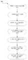
도 5는 본 개시에 따른 결함 검사를 수행하는 방법을 예시한다.
도 6은 다이 상에 드로잉되는 케어 영역들을 예시한다.
도 7은 검사될 다이에 피팅되는(fitted) 케어 영역들을 예시한다.
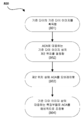
도 8은 본 개시에 따른 적응형 케어 영역에 대한 예비적 조정을 수행하는 방법을 예시한다.
도 9는 본 개시의 시스템 실시예를 예시한다.
도 10은 본 개시의 다른 시스템 실시예를 예시한다.
도 11은 케어 영역으로 인한 결함 보고와 본 개시의 일 실시예에서 적응형 케어 영역과의 비교를 예시한다.
도 12는 케어 영역이 오정렬되는 케어 영역 정렬을 예시한다.
도 13은 본 개시의 일 실시예에 따른 ACA 정렬을 예시한다.
Claims (20)
- 결함 검사를 수행하는 방법에 있어서,
적어도 하나의 적응형 케어 영역(adaptive care area)을 정의하는 단계로서, 상기 적응형 케어 영역은,
x-좌표;
y-좌표; 및
형상
을 포함하는 복수의 미리 결정된 속성들(properties)을 갖는 것인, 상기 정의하는 단계;
상기 적응형 케어 영역을 레시피에 저장하는 단계 - 상기 레시피는 전자 데이터 저장 유닛 내에 저장됨 - ;
입자 방출기 및 검출기를 포함하는 검사 도구를 사용하여 스테이지 상의 웨이퍼의 다이 이미지를 획득하는 단계; 및
프로세서에서, 상기 전자 데이터 저장 유닛으로부터 상기 레시피를 판독하고,
상기 적응형 케어 영역에 대응하는 상기 다이 이미지 상의 제1 위치를 결정하는 것;
상기 다이 이미지 상의 상기 제1 위치 상에 상기 적응형 케어 영역을 오버레이하는 것;
상기 적응형 케어 영역을 상기 다이 이미지 상의 하나 이상의 대응하는 특징부(feature)로 조정하는 것; 및
상기 적응형 케어 영역 내에서 상기 다이 이미지의 결함 검사를 수행하는 것
에 의해 상기 레시피에 저장된 상기 적응형 케어 영역에 대해 상기 프로세서를 사용하는 단계
를 포함하는, 결함 검사를 수행하는 방법. - 제1항에 있어서,
상기 입자 방출기는 광대역 플라즈마 소스, 전자 빔 소스, 램프 또는 레이저를 포함하는 것인, 결함 검사를 수행하는 방법. - 제1항에 있어서,
상기 형상은 다각형 또는 타원형인 것인, 결함 검사를 수행하는 방법. - 제1항에 있어서,
상기 형상은 사용자-정의된 불규칙한 형상인 것인, 결함 검사를 수행하는 방법. - 제1항에 있어서,
상기 복수의 미리 결정된 속성들은 적어도 하나의 특징부 속성을 더 포함하는 것인, 결함 검사를 수행하는 방법. - 제5항에 있어서,
상기 특징부 속성은, 스케일링된 불변 특징부 변환, 가속된 견고한 특징부, 배향되고 회전된 브리프(brief), 배향된 그래디언트들의 히스토그램, 코너-검출기 또는 그래디언트-기반 디스크립터(descriptor)를 포함하는 것인, 결함 검사를 수행하는 방법. - 제1항에 있어서,
상기 적응형 케어 영역을 상기 다이 이미지 상의 하나 이상의 대응하는 특징부로 조정하는 것은, 병진, 회전, 스케일링, 아핀(affine) 변환, 관점 워핑(warping) 또는 투사 왜곡 중 하나 이상을 포함하는 것인, 결함 검사를 수행하는 방법. - 제1항에 있어서,
하나 이상의 조정 제한(adjustment limit)을 결정하는 단계를 더 포함하고, 상기 적응형 케어 영역을 상기 다이 이미지 내의 하나 이상의 대응하는 특징부로 조정하는 것은 상기 하나 이상의 조정 제한에 의해 제한되는 것인, 결함 검사를 수행하는 방법. - 제1항에 있어서,
상기 형상은 다각형이고, 상기 적응형 케어 영역을 상기 다이 이미지 상의 상기 하나 이상의 대응하는 특징부로 조정하는 것은 상기 다각형의 적어도 하나의 코너를 조정하는 것을 포함하는 것인, 결함 검사를 수행하는 방법. - 제9항에 있어서,
하나 이상의 조정 제한을 결정하는 단계를 더 포함하고, 상기 다각형의 코너를 조정하는 것은 상기 하나 이상의 조정 제한에 의해 제한되는 것인, 결함 검사를 수행하는 방법. - 제1항에 있어서,
상기 다이 이미지를 획득하기 위해 상기 검사 도구를 사용하기 전에 상기 적응형 케어 영역에 예비적 조정(preliminary adjustment)을 수행하는 단계를 더 포함하고, 상기 적응형 케어 영역에 대한 상기 예비적 조정은,
기준 다이의 기준 다이 이미지를 획득하는 것 - 상기 기준 다이는 검증된 특징부들을 갖는 골든 다이, 이웃 다이들의 중앙값으로부터 계산된 합성 다이, 또는 설계 파일로부터 시뮬레이트된 설계 이미지임 - ; 및
상기 프로세서에서, 상기 전자 데이터 저장 유닛으로부터 상기 레시피를 판독하고,
상기 적응형 케어 영역에 대응하는 상기 기준 다이 이미지 상의 제2 위치를 결정하는 것,
상기 기준 다이 이미지 상의 상기 제2 위치 상에 상기 적응형 케어 영역을 오버레이하는 것, 및
상기 적응형 케어 영역을 상기 기준 다이 이미지 상의 하나 이상의 대응하는 요소로 예비적으로 조정하는 것
에 의해 상기 레시피에 세이브된 상기 적응형 케어 영역에 대해 상기 프로세서를 사용하는 것
을 포함하는 것인, 결함 검사를 수행하는 방법. - 결함 검사 시스템에 있어서,
검사 도구;
전자 데이터 저장 유닛; 및
프로세서를 포함하고,
상기 검사 도구는,
입자 빔에서 입자들을 방출하도록 구성되는 입자 방출기,
상기 입자 방출기에 의해 방출된 상기 입자 빔의 경로에서 웨이퍼를 유지하도록 구성되는 스테이지, 및
상기 웨이퍼에 의해 반사된 입자들의 일부분을 검출하고 다이 이미지를 도출하도록 구성되는 검출기
를 포함하고,
상기 전자 데이터 저장 유닛은, 레시피를 저장하도록 구성되고, 상기 레시피는 적어도 하나의 적응형 케어 영역을 포함하며, 상기 적응형 케어 영역은,
x-좌표,
y-좌표, 및
형상
을 포함하는 복수의 미리 결정된 속성들을 갖고;
상기 프로세서는, 상기 검사 도구 및 상기 전자 데이터 저장 유닛과 전자 통신하며,
상기 검사 도구로부터 상기 다이 이미지를 수신하고;
상기 전자 데이터 저장 유닛으로부터 상기 레시피를 판독하고, 상기 레시피에 세이브된 각각의 적응형 케어 영역에 대해,
상기 적응형 케어 영역에 대응하는 상기 다이 이미지 상의 제1 위치를 결정하고,
상기 다이 이미지 상의 상기 제1 위치 상에 상기 적응형 케어 영역을 오버레이하고;
상기 적응형 케어 영역을 상기 다이 이미지 상의 하나 이상의 대응하는 요소로 조정하고;
상기 적응형 케어 영역 내에서 상기 다이 이미지의 결함 검사를 수행하도록
구성되는 것인, 결함 검사 시스템. - 제12항에 있어서,
상기 프로세서는 또한, 상기 전자 데이터 저장 유닛으로부터 상기 레시피를 판독하고, 상기 레시피에 세이브된 상기 적응형 케어 영역에 대해,
상기 적응형 케어 영역에 대응하는 기준 다이 이미지의 제2 위치를 결정하고 - 상기 기준 다이 이미지는 검증된 특징부들을 갖는 골든 다이, 이웃 다이들의 중앙값으로부터 계산된 합성 다이, 또는 설계 파일로부터 시뮬레이트된 설계 이미지로부터 획득됨 -;
상기 기준 다이 이미지 상의 상기 제2 위치 상에 상기 적응형 케어 영역을 오버레이하고;
상기 적응형 케어 영역을 상기 기준 다이 이미지 상의 하나 이상의 대응하는 특징부로 예비적으로 조정하도록
구성되는 것인, 결함 검사 시스템. - 제12항에 있어서,
상기 입자들은 광자들 또는 전자들인 것인, 결함 검사 시스템. - 제12항에 있어서,
상기 형상은 다각형 또는 타원형인 것인, 결함 검사 시스템. - 제12항에 있어서,
상기 형상은 사용자-정의된 불규칙한 형상인 것인, 결함 검사 시스템. - 비일시적 컴퓨터 판독가능 저장 매체에 있어서,
하나 이상의 컴퓨팅 디바이스들 상에서,
적응형 케어 영역을 정의하는 단계 - 상기 적응형 케어 영역은, x-좌표; y-좌표; 및 형상을 포함하는 복수의 미리 결정된 속성들을 가짐 -;
상기 적응형 케어 영역을 레시피에 세이브하는 단계;
입자 방출기 및 검출기를 포함하는 검사 도구로부터, 스테이지 상의 웨이퍼로부터 다이 이미지를 획득하는 단계; 및
상기 레시피를 판독하고, 상기 레시피에 세이브된 각각의 적응형 케어 영역에 대해,
상기 적응형 케어 영역에 대응하는 상기 다이 이미지 상의 위치를 결정하는 단계;
상기 다이 이미지 상의 상기 위치 상에 상기 적응형 케어 영역을 오버레이하는 단계;
상기 적응형 케어 영역을 상기 다이 이미지 상의 하나 이상의 대응하는 특징부로 조정하는 단계; 및
상기 적응형 케어 영역 내에서 상기 다이 이미지의 결함 검사를 수행하도록 하는 명령들을 전송하는 단계
를 실행하기 위한 하나 이상의 프로그램을 포함하는, 비일시적 컴퓨터 판독가능 저장 매체. - 제17항에 있어서,
상기 형상은 다각형 또는 타원형인 것인, 비일시적 컴퓨터 판독가능 저장 매체. - 제17항에 있어서,
상기 형상은 사용자-정의된 불규칙한 형상인 것인, 비일시적 컴퓨터 판독가능 저장 매체. - 제17항에 있어서,
하나 이상의 조정 제한이 결정되고, 상기 적응형 케어 영역을 상기 다이 이미지 내의 하나 이상의 대응하는 특징부로 조정하는 단계는 상기 하나 이상의 조정 제한에 의해 제한되는 것인, 비일시적 컴퓨터 판독가능 저장 매체.
Applications Claiming Priority (5)
| Application Number | Priority Date | Filing Date | Title |
|---|---|---|---|
| US201762574189P | 2017-10-18 | 2017-10-18 | |
| US62/574,189 | 2017-10-18 | ||
| US16/158,774 | 2018-10-12 | ||
| US16/158,774 US10997710B2 (en) | 2017-10-18 | 2018-10-12 | Adaptive care areas for die-die inspection |
| PCT/US2018/056209 WO2019079389A1 (en) | 2017-10-18 | 2018-10-17 | ADAPTIVE REFERENCE AREAS FOR CHIP INSPECTION |
Publications (2)
| Publication Number | Publication Date |
|---|---|
| KR20200058575A true KR20200058575A (ko) | 2020-05-27 |
| KR102408317B1 KR102408317B1 (ko) | 2022-06-10 |
Family
ID=66096572
Family Applications (1)
| Application Number | Title | Priority Date | Filing Date |
|---|---|---|---|
| KR1020207014020A Active KR102408317B1 (ko) | 2017-10-18 | 2018-10-17 | 다이-다이 검사를 위한 적응형 케어 영역들 |
Country Status (7)
| Country | Link |
|---|---|
| US (1) | US10997710B2 (ko) |
| EP (1) | EP3698397A4 (ko) |
| JP (2) | JP2021500742A (ko) |
| KR (1) | KR102408317B1 (ko) |
| CN (1) | CN111194479B (ko) |
| TW (1) | TWI761612B (ko) |
| WO (1) | WO2019079389A1 (ko) |
Families Citing this family (8)
| Publication number | Priority date | Publication date | Assignee | Title |
|---|---|---|---|---|
| US11220856B2 (en) | 2019-04-03 | 2022-01-11 | The Chamberlain Group Llc | Movable barrier operator enhancement device and method |
| US11127136B2 (en) * | 2019-12-05 | 2021-09-21 | Kla Corporation | System and method for defining flexible regions on a sample during inspection |
| US11610296B2 (en) * | 2020-01-09 | 2023-03-21 | Kla Corporation | Projection and distance segmentation algorithm for wafer defect detection |
| US12165306B2 (en) * | 2021-03-16 | 2024-12-10 | Kla Corporation | Segmentation of design care areas with a rendered design image |
| CN116057350A (zh) * | 2021-07-14 | 2023-05-02 | 株式会社日立高新技术 | 轮廓线解析装置、加工尺寸提取系统、处理条件决定系统、半导体装置制造系统以及数据结构 |
| DE102021119008A1 (de) * | 2021-07-30 | 2023-02-02 | Carl Zeiss Multisem Gmbh | Verfahren zur Defekterkennung in einer Halbleiterprobe bei Probenbildern mit Verzeichnung |
| US20250232512A1 (en) * | 2024-01-17 | 2025-07-17 | Nvidia Corporation | Pixel generation technique |
| US20250277752A1 (en) * | 2024-03-04 | 2025-09-04 | Taiwan Semiconductor Manufacturing Company, Ltd. | Optical inspection system, method of optical inspection, and method of manufacturing semiconductor package |
Citations (3)
| Publication number | Priority date | Publication date | Assignee | Title |
|---|---|---|---|---|
| US20100246931A1 (en) * | 2009-03-30 | 2010-09-30 | Koh Young Technology Inc. | Inspection method |
| US20140376802A1 (en) * | 2013-06-21 | 2014-12-25 | Kla-Tencor Corporation | Wafer Inspection Using Free-Form Care Areas |
| JP2017529684A (ja) * | 2014-07-22 | 2017-10-05 | ケーエルエー−テンカー コーポレイション | 被検査物上の関心対象領域の座標決定 |
Family Cites Families (15)
| Publication number | Priority date | Publication date | Assignee | Title |
|---|---|---|---|---|
| JPH05150442A (ja) | 1991-11-27 | 1993-06-18 | Nikon Corp | 異物検査装置 |
| US10354405B2 (en) * | 2010-05-17 | 2019-07-16 | Kla-Tencor Corporation | Run-time correction of defect locations during defect review |
| JP5941782B2 (ja) * | 2012-07-27 | 2016-06-29 | 株式会社日立ハイテクノロジーズ | マッチング処理装置、マッチング処理方法、及びそれを用いた検査装置 |
| US9189844B2 (en) * | 2012-10-15 | 2015-11-17 | Kla-Tencor Corp. | Detecting defects on a wafer using defect-specific information |
| US9429856B1 (en) | 2013-01-21 | 2016-08-30 | Kla-Tencor Corporation | Detectable overlay targets with strong definition of center locations |
| US9092846B2 (en) * | 2013-02-01 | 2015-07-28 | Kla-Tencor Corp. | Detecting defects on a wafer using defect-specific and multi-channel information |
| US9715725B2 (en) * | 2013-12-21 | 2017-07-25 | Kla-Tencor Corp. | Context-based inspection for dark field inspection |
| US10127652B2 (en) * | 2014-02-06 | 2018-11-13 | Kla-Tencor Corp. | Defect detection and classification based on attributes determined from a standard reference image |
| US9401016B2 (en) * | 2014-05-12 | 2016-07-26 | Kla-Tencor Corp. | Using high resolution full die image data for inspection |
| US10393671B2 (en) * | 2015-04-29 | 2019-08-27 | Kla-Tencor Corp. | Intra-die defect detection |
| US10359371B2 (en) * | 2015-08-24 | 2019-07-23 | Kla-Tencor Corp. | Determining one or more characteristics of a pattern of interest on a specimen |
| TWI684225B (zh) * | 2015-08-28 | 2020-02-01 | 美商克萊譚克公司 | 自定向計量和圖樣分類 |
| TWI583941B (zh) * | 2015-10-01 | 2017-05-21 | 萬潤科技股份有限公司 | Grain defect detection method and device |
| JP2017129369A (ja) | 2016-01-18 | 2017-07-27 | 株式会社東芝 | 欠陥検査装置、欠陥検査方法、および欠陥検査プログラム |
| CN106600600A (zh) * | 2016-12-26 | 2017-04-26 | 华南理工大学 | 基于特征匹配的晶圆缺陷检测方法 |
-
2018
- 2018-10-12 US US16/158,774 patent/US10997710B2/en active Active
- 2018-10-17 JP JP2020521368A patent/JP2021500742A/ja active Pending
- 2018-10-17 CN CN201880065545.7A patent/CN111194479B/zh active Active
- 2018-10-17 KR KR1020207014020A patent/KR102408317B1/ko active Active
- 2018-10-17 WO PCT/US2018/056209 patent/WO2019079389A1/en not_active Ceased
- 2018-10-17 EP EP18868380.9A patent/EP3698397A4/en active Pending
- 2018-10-18 TW TW107136646A patent/TWI761612B/zh active
-
2022
- 2022-09-22 JP JP2022151488A patent/JP7454620B2/ja active Active
Patent Citations (3)
| Publication number | Priority date | Publication date | Assignee | Title |
|---|---|---|---|---|
| US20100246931A1 (en) * | 2009-03-30 | 2010-09-30 | Koh Young Technology Inc. | Inspection method |
| US20140376802A1 (en) * | 2013-06-21 | 2014-12-25 | Kla-Tencor Corporation | Wafer Inspection Using Free-Form Care Areas |
| JP2017529684A (ja) * | 2014-07-22 | 2017-10-05 | ケーエルエー−テンカー コーポレイション | 被検査物上の関心対象領域の座標決定 |
Also Published As
| Publication number | Publication date |
|---|---|
| CN111194479A (zh) | 2020-05-22 |
| WO2019079389A1 (en) | 2019-04-25 |
| JP2022179533A (ja) | 2022-12-02 |
| US10997710B2 (en) | 2021-05-04 |
| EP3698397A4 (en) | 2021-07-21 |
| CN111194479B (zh) | 2023-10-27 |
| JP7454620B2 (ja) | 2024-03-22 |
| TW201928338A (zh) | 2019-07-16 |
| JP2021500742A (ja) | 2021-01-07 |
| TWI761612B (zh) | 2022-04-21 |
| KR102408317B1 (ko) | 2022-06-10 |
| US20190114758A1 (en) | 2019-04-18 |
| EP3698397A1 (en) | 2020-08-26 |
Similar Documents
| Publication | Publication Date | Title |
|---|---|---|
| JP7454620B2 (ja) | ダイ・ダイ検査用適応性ケアエリア | |
| US20190026596A1 (en) | Pattern inspection apparatus and pattern inspection method | |
| KR102684035B1 (ko) | 검사 및 다른 프로세스를 위한 시료의 정렬 | |
| TWI907462B (zh) | 用於半導體缺陷檢視之方法及系統以及相關之非暫時電腦可讀儲存媒體 | |
| TW202208836A (zh) | 用於雜訊影像之影像對準 | |
| WO2022046825A1 (en) | Setting up inspection of a specimen | |
| CN117355930B (zh) | 通过基于图像投影的修补对设计对准的晶片对准改进 | |
| US11783470B2 (en) | Design-assisted inspection for DRAM and 3D NAND devices | |
| TWI851819B (zh) | 半導體檢測的系統及方法,以及非暫時性電腦可讀媒體 | |
| US11610296B2 (en) | Projection and distance segmentation algorithm for wafer defect detection | |
| JP2024537955A (ja) | レーザアニールパターンの抑制 | |
| US20260029725A1 (en) | Localized region of interest based image grabs for improved metrology cost of ownership | |
| TW202104829A (zh) | 將絕對z高度值用於工具之間的協同作用之技術 | |
| US11776859B2 (en) | Care area based swath speed for throughput and sensitivity improvement | |
| CN119379799A (zh) | 一种半导体机台量测定位方法及半导体机台 |
Legal Events
| Date | Code | Title | Description |
|---|---|---|---|
| PA0105 | International application |
St.27 status event code: A-0-1-A10-A15-nap-PA0105 |
|
| PG1501 | Laying open of application |
St.27 status event code: A-1-1-Q10-Q12-nap-PG1501 |
|
| A201 | Request for examination | ||
| A302 | Request for accelerated examination | ||
| P11-X000 | Amendment of application requested |
St.27 status event code: A-2-2-P10-P11-nap-X000 |
|
| P13-X000 | Application amended |
St.27 status event code: A-2-2-P10-P13-nap-X000 |
|
| PA0201 | Request for examination |
St.27 status event code: A-1-2-D10-D11-exm-PA0201 |
|
| PA0302 | Request for accelerated examination |
St.27 status event code: A-1-2-D10-D17-exm-PA0302 St.27 status event code: A-1-2-D10-D16-exm-PA0302 |
|
| E902 | Notification of reason for refusal | ||
| PE0902 | Notice of grounds for rejection |
St.27 status event code: A-1-2-D10-D21-exm-PE0902 |
|
| P11-X000 | Amendment of application requested |
St.27 status event code: A-2-2-P10-P11-nap-X000 |
|
| P13-X000 | Application amended |
St.27 status event code: A-2-2-P10-P13-nap-X000 |
|
| E701 | Decision to grant or registration of patent right | ||
| PE0701 | Decision of registration |
St.27 status event code: A-1-2-D10-D22-exm-PE0701 |
|
| GRNT | Written decision to grant | ||
| PR0701 | Registration of establishment |
St.27 status event code: A-2-4-F10-F11-exm-PR0701 |
|
| PR1002 | Payment of registration fee |
St.27 status event code: A-2-2-U10-U12-oth-PR1002 Fee payment year number: 1 |
|
| PG1601 | Publication of registration |
St.27 status event code: A-4-4-Q10-Q13-nap-PG1601 |
|
| PR1001 | Payment of annual fee |
St.27 status event code: A-4-4-U10-U11-oth-PR1001 Fee payment year number: 4 |
|
| P22-X000 | Classification modified |
St.27 status event code: A-4-4-P10-P22-nap-X000 |